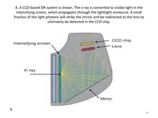
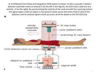
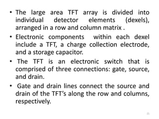
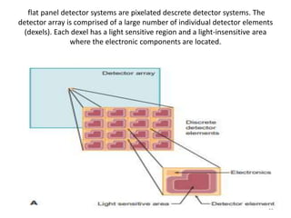
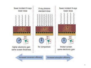
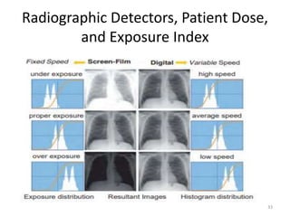
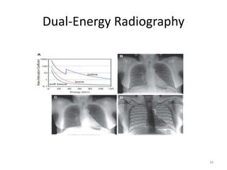
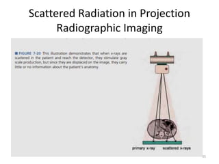
JAI HIND
1
STUDENT:- FACULTY:-
VIRENDRA K.MAURYA Ms.PRIYANKA MAM
M.Sc.(RIT) (INCHARGE & HEAD OF RIT)
2
COMPUTED RADIOGRAPHY (CR)
COMPUTED RADIOGRAPHY
• Computed radiography (CR) refers to photostimulable
phosphor detector (PSP) systems, which are historically
housed in a cassette similar to a screen-film cassette.
• Traditional scintillators, such as Gd₂O₂ S and cesium
iodide (CsI), emit light promptly (nearly
instantaneously) when irradiated by an x-ray beam.
• When x-rays are absorbed by photostimulable
phosphors, some light is also promptly emitted, but a
fraction of the absorbed x-ray energy is trapped in the
PSP screen and can be read out later using laser light.
•
3
• For this reason, PSP screens are also called storage
phosphors.
• CR was introduced in the 1970s, saw increasing use in
the late 1980s, and was in wide use at the turn of the
century as many departments installed PACS.
• Most CR imaging plates are composed of a mixture of
BaFBr and other halidebased phosphors, often referred
to as barium fluorohalide.
• A CR plate is a flexible screen that is enclosed in a light-
tight cassette.
• The CR cassette is exposed to x-rays during the
radiographic examination and is subsequently placed in
a CR reader.
• Once placed in the CR reader, the following steps take
place:
4
• 1. The cassette is moved into the reader unit, and
the imaging plate is mechanically removed from
the cassette.
• 2. The imaging plate is translated vertically in the
(y) direction by rollers across a moving stage and
is scanned horizontally in the (x) direction by a
laser beam of approximately 700 nm wavelength.
• 3. Red laser light stimulates the emission of
trapped energy in a tiny area (x,y location) of the
imaging plate, and blue-green visible light is
emitted from the storage phosphor as energetic
electrons drop down to their ground state.
5
• 4. The light emitted through photostimulated
luminescence is collected by a fiber optic light
guide and strikes a photomultiplier tube (PMT),
where it produces an electronic signal.
• 5. The electronic signal is digitized and stored as a
pixel value. For every spatial location (x, y) on the
imaging plate, a corresponding gray scale value is
determined that is proportional to the locally
absorbed x-ray energy.
• 6. The plate is exposed to bright white light to
erase any residual trapped energy.
• 7. The imaging plate is returned to the cassette
and is ready for reuse.
6
• The digital image that is generated by the CR
reader is stored temporarily on a local hard
disk.
• Once acquired, the digital radiographic image
undergoes image processing by the CR reader.
• The image is then typically sent to a PACS for
interpretation by a radiologist and long-term
archiving.
7
8
The readout mechanics of a
CR system are shown. The
imaging plate is translated
through the mechanism by a
series of rollers, and a laser
beam scans horizontally
across the plate.
The rotating multifaceted
mirror causes the laser
beam to scan the imaging
plate in a raster fashion.
The light released by laser
stimulation is collected by
the light guide and produces
a signal in the PMT. The red
light from the laser is
filtered out before reaching
the PMT
• the blue light that is emitted from the screen
has shorter wavelength and higher energy per
photon than the stimulating red light.
9
• Typical imaging plates are composed of about
85% BaFBr and 15% BaFI, activated with a small
quantity of europium.
• The CR screen is amorphous (lacks structure); the
barium fluorohalide crystals are small and are
held together by an inert, optically transparent
binder.
• The nomenclature BaFBr:Eu indicates that the
BaFBr phosphor is activated by europium. This
activation procedure, also called doping, creates
defects in the BaFBr crystals that allow electrons
to be trapped more efficiently.
• The defects in the crystalline lattice caused by the
europium dopant give rise to so-called F-centers
10
11
• A. During exposure, x-rays are absorbed in the
storage phosphor and some of the electrons
reach the conduction band, where they may
interact with an F-center, causing the
reduction of europium (Eu) ions.
B. The electrons are trapped in this high-energy,
metastable state, and can remain there for
minutes to months.
C. the F-center releases a trapped electron, the
trivalent europium (Eu⁺³) is converted back to
its divalent state. (Eu⁺²)
12
13
Charge-Coupled Device and Complementary
Metal-Oxide Semiconductor detectors
• Charge-coupled device (CCD) detectors form
images from visible light .
• CCD detectors are used in commercial-grade
television cameras and in scientific
applications such as astronomy.
14
• The CCD chip itself is an integrated circuit made
of crystalline silicon, as is the central processing
unit of a computer.
• A CCD chip has an array of discrete detector
electronics etched into its surface.
• The silicon surface of a CCD chip is
photosensitive—as visible light falls on each
dexel, electrons are liberated and build up in the
dexel.
• More electrons are produced in dexels that
receive more intense light.
• The electrons are confined to each dexel because
there are electronic barriers (voltage) on each
side of the dexel during exposure
15
. A photograph of a high-resolution
CCD chip is shown
16
B. The readout procedure in a CCD chip is illustrated.
C. This illustration shows the shift of a given pattern of
exposure down one column in a CCD chip in four (t1–
t4) successive clock cycles
17
A. A CCD-based DR system is shown. The x-ray is converted to visible light in the
intensifying screen, which propagates through the lighttight enclosure. A small
fraction of the light photons will strike the mirror and be redirected to the lens to
ultimately be detected in the CCD chip.
18
. B. A CCDbased Time Delay and Integration (TDI) system is shown. As the x-ray tube / slitslot /
detector assembly moves at velocity V (to the left in this figure), the CCD chip is read-out at a
velocity −V (to the right). By synchronizing the velocity of the read out with the scanning motion,
the signal region under an object in the patient travels across the entire field of view of the
detector, and its contrast signal is built up across all of the dexels in the TDI CCD chip
19
Flat Panel Thin-Film-Transistor Array
Detectors
• Flat panel Thin-Film-Transistor (TFT) array
detectors make use of technology similar to that
used in flat panel displays, and much of this has
to do with the wiring requirements of a huge
number of individual display elements.
• Flat-panel TFT arrays are made of amorphous
silicon, where lithographic etching techniques are
used to deposit electronic components and
connections necessary for x-ray detector
operation.
20
• The large area TFT array is divided into
individual detector elements (dexels),
arranged in a row and column matrix .
• Electronic components within each dexel
include a TFT, a charge collection electrode,
and a storage capacitor.
• The TFT is an electronic switch that is
comprised of three connections: gate, source,
and drain.
• Gate and drain lines connect the source and
drain of the TFT’s along the row and columns,
respectively.
21
flat panel detector systems are pixelated descrete detector systems. The
detector array is comprised of a large number of individual detector elements
(dexels). Each dexel has a light sensitive region and a light-insensitive area
where the electronic components are located.
22
A photomicrograph of an actual TFT system is shown. The electronics
component can be seen in the upper left corner of each dexel (Image
courtesy John Sabol and Bill Hennessy, GE Healthcare
23
Indirect Detection TFT Arrays
24
This diagram shows circuitry for a TFT flat panel
detector system. The readout process is described in the
text
Indirect and direct detector TFT–
based x-ray detectors are shown
25
• Direct Detection TFT Arrays:-
• Direct x-ray conversion TFT arrays use a semiconductor material
that produces electron-hole pairs in proportion to the incident x-ray
intensity.
• Absorbed x-ray energy is directly converted into charge in the
detector
• - there is no intermediate step involving the production of visible
light photons.
• Amorphous selenium (a-Se) is the semiconductor most widely used,
and is layered between two surface-area electrodes connected to
the bias voltage and a dielectric layer.
• The dielectric layer prevents overcharging dexels, which could
damage the TFT array.
• Ion pairs are collected under applied voltage across the solid state
converter (10–50 V/mum of thickness).
• In addition to selenium, other materials such as mercuric iodide
(HgI₂ ), lead iodide (PbI₂ ), and cadmium telluride (CdTe) are being
studied for use in direct detection flat panel systems.
26
Technique Factors in Radiography
• the principal x-ray technique factors used for
radiography include the tube voltage (the kV), the
tube current (mA), the exposure time, and the x-
ray source-to-image distance, SID. The SID is
standardized to 100 cm typically , and 183 cm for
upright chest radiography.
• In general, lower kV settings will increase the
dose to the patient compared to higher kV
settings for the same imaging procedure and
same body part, but the trade-off is that subject
contrast is reduced with higher kV.
27
28
Scintillators and Intensifying Screens
• An indirect x-ray detector system uses a scintillator to
convert the x-ray fluence incident on the detector into
a visible light signal, which is then used to expose the
emulsion in screen-film radiography or a
photoconductor in digital radiographic systems.
• Over the long history of screen-film radiography, a
number of scintillators were developed.
• Most intensifying screens are comprised of fine-grain
crystalline scintillating powders (also called phosphors),
formed into a uniformly thick intensifying screen that is
held together by a binder.
29
Absorption Efficiency and Conversion
Efficiency
• Because of the dynamics of indirect x-ray
detection described above, there are two
factors that are important in x-ray detectors.
30
31
Other Considerations
• CR is often the first digital radiographic
system installed in a hospital, because it can
directly replace screen-film cassettes in
existing radiography units and in portable,
bedside examinations, where the cost of
retakes in both technologist time and money
is high.
32
Radiographic Detectors, Patient Dose,
and Exposure Index
33
Dual-Energy Radiography
34
Scattered Radiation in Projection
Radiographic Imaging
35
36

cr srms1.pptx

  • 1.
  • 2.
    STUDENT:- FACULTY:- VIRENDRA K.MAURYAMs.PRIYANKA MAM M.Sc.(RIT) (INCHARGE & HEAD OF RIT) 2 COMPUTED RADIOGRAPHY (CR)
  • 3.
    COMPUTED RADIOGRAPHY • Computedradiography (CR) refers to photostimulable phosphor detector (PSP) systems, which are historically housed in a cassette similar to a screen-film cassette. • Traditional scintillators, such as Gd₂O₂ S and cesium iodide (CsI), emit light promptly (nearly instantaneously) when irradiated by an x-ray beam. • When x-rays are absorbed by photostimulable phosphors, some light is also promptly emitted, but a fraction of the absorbed x-ray energy is trapped in the PSP screen and can be read out later using laser light. • 3
  • 4.
    • For thisreason, PSP screens are also called storage phosphors. • CR was introduced in the 1970s, saw increasing use in the late 1980s, and was in wide use at the turn of the century as many departments installed PACS. • Most CR imaging plates are composed of a mixture of BaFBr and other halidebased phosphors, often referred to as barium fluorohalide. • A CR plate is a flexible screen that is enclosed in a light- tight cassette. • The CR cassette is exposed to x-rays during the radiographic examination and is subsequently placed in a CR reader. • Once placed in the CR reader, the following steps take place: 4
  • 5.
    • 1. Thecassette is moved into the reader unit, and the imaging plate is mechanically removed from the cassette. • 2. The imaging plate is translated vertically in the (y) direction by rollers across a moving stage and is scanned horizontally in the (x) direction by a laser beam of approximately 700 nm wavelength. • 3. Red laser light stimulates the emission of trapped energy in a tiny area (x,y location) of the imaging plate, and blue-green visible light is emitted from the storage phosphor as energetic electrons drop down to their ground state. 5
  • 6.
    • 4. Thelight emitted through photostimulated luminescence is collected by a fiber optic light guide and strikes a photomultiplier tube (PMT), where it produces an electronic signal. • 5. The electronic signal is digitized and stored as a pixel value. For every spatial location (x, y) on the imaging plate, a corresponding gray scale value is determined that is proportional to the locally absorbed x-ray energy. • 6. The plate is exposed to bright white light to erase any residual trapped energy. • 7. The imaging plate is returned to the cassette and is ready for reuse. 6
  • 7.
    • The digitalimage that is generated by the CR reader is stored temporarily on a local hard disk. • Once acquired, the digital radiographic image undergoes image processing by the CR reader. • The image is then typically sent to a PACS for interpretation by a radiologist and long-term archiving. 7
  • 8.
    8 The readout mechanicsof a CR system are shown. The imaging plate is translated through the mechanism by a series of rollers, and a laser beam scans horizontally across the plate. The rotating multifaceted mirror causes the laser beam to scan the imaging plate in a raster fashion. The light released by laser stimulation is collected by the light guide and produces a signal in the PMT. The red light from the laser is filtered out before reaching the PMT
  • 9.
    • the bluelight that is emitted from the screen has shorter wavelength and higher energy per photon than the stimulating red light. 9
  • 10.
    • Typical imagingplates are composed of about 85% BaFBr and 15% BaFI, activated with a small quantity of europium. • The CR screen is amorphous (lacks structure); the barium fluorohalide crystals are small and are held together by an inert, optically transparent binder. • The nomenclature BaFBr:Eu indicates that the BaFBr phosphor is activated by europium. This activation procedure, also called doping, creates defects in the BaFBr crystals that allow electrons to be trapped more efficiently. • The defects in the crystalline lattice caused by the europium dopant give rise to so-called F-centers 10
  • 11.
  • 12.
    • A. Duringexposure, x-rays are absorbed in the storage phosphor and some of the electrons reach the conduction band, where they may interact with an F-center, causing the reduction of europium (Eu) ions. B. The electrons are trapped in this high-energy, metastable state, and can remain there for minutes to months. C. the F-center releases a trapped electron, the trivalent europium (Eu⁺³) is converted back to its divalent state. (Eu⁺²) 12
  • 13.
  • 14.
    Charge-Coupled Device andComplementary Metal-Oxide Semiconductor detectors • Charge-coupled device (CCD) detectors form images from visible light . • CCD detectors are used in commercial-grade television cameras and in scientific applications such as astronomy. 14
  • 15.
    • The CCDchip itself is an integrated circuit made of crystalline silicon, as is the central processing unit of a computer. • A CCD chip has an array of discrete detector electronics etched into its surface. • The silicon surface of a CCD chip is photosensitive—as visible light falls on each dexel, electrons are liberated and build up in the dexel. • More electrons are produced in dexels that receive more intense light. • The electrons are confined to each dexel because there are electronic barriers (voltage) on each side of the dexel during exposure 15
  • 16.
    . A photographof a high-resolution CCD chip is shown 16
  • 17.
    B. The readoutprocedure in a CCD chip is illustrated. C. This illustration shows the shift of a given pattern of exposure down one column in a CCD chip in four (t1– t4) successive clock cycles 17
  • 18.
    A. A CCD-basedDR system is shown. The x-ray is converted to visible light in the intensifying screen, which propagates through the lighttight enclosure. A small fraction of the light photons will strike the mirror and be redirected to the lens to ultimately be detected in the CCD chip. 18
  • 19.
    . B. ACCDbased Time Delay and Integration (TDI) system is shown. As the x-ray tube / slitslot / detector assembly moves at velocity V (to the left in this figure), the CCD chip is read-out at a velocity −V (to the right). By synchronizing the velocity of the read out with the scanning motion, the signal region under an object in the patient travels across the entire field of view of the detector, and its contrast signal is built up across all of the dexels in the TDI CCD chip 19
  • 20.
    Flat Panel Thin-Film-TransistorArray Detectors • Flat panel Thin-Film-Transistor (TFT) array detectors make use of technology similar to that used in flat panel displays, and much of this has to do with the wiring requirements of a huge number of individual display elements. • Flat-panel TFT arrays are made of amorphous silicon, where lithographic etching techniques are used to deposit electronic components and connections necessary for x-ray detector operation. 20
  • 21.
    • The largearea TFT array is divided into individual detector elements (dexels), arranged in a row and column matrix . • Electronic components within each dexel include a TFT, a charge collection electrode, and a storage capacitor. • The TFT is an electronic switch that is comprised of three connections: gate, source, and drain. • Gate and drain lines connect the source and drain of the TFT’s along the row and columns, respectively. 21
  • 22.
    flat panel detectorsystems are pixelated descrete detector systems. The detector array is comprised of a large number of individual detector elements (dexels). Each dexel has a light sensitive region and a light-insensitive area where the electronic components are located. 22
  • 23.
    A photomicrograph ofan actual TFT system is shown. The electronics component can be seen in the upper left corner of each dexel (Image courtesy John Sabol and Bill Hennessy, GE Healthcare 23
  • 24.
    Indirect Detection TFTArrays 24 This diagram shows circuitry for a TFT flat panel detector system. The readout process is described in the text
  • 25.
    Indirect and directdetector TFT– based x-ray detectors are shown 25
  • 26.
    • Direct DetectionTFT Arrays:- • Direct x-ray conversion TFT arrays use a semiconductor material that produces electron-hole pairs in proportion to the incident x-ray intensity. • Absorbed x-ray energy is directly converted into charge in the detector • - there is no intermediate step involving the production of visible light photons. • Amorphous selenium (a-Se) is the semiconductor most widely used, and is layered between two surface-area electrodes connected to the bias voltage and a dielectric layer. • The dielectric layer prevents overcharging dexels, which could damage the TFT array. • Ion pairs are collected under applied voltage across the solid state converter (10–50 V/mum of thickness). • In addition to selenium, other materials such as mercuric iodide (HgI₂ ), lead iodide (PbI₂ ), and cadmium telluride (CdTe) are being studied for use in direct detection flat panel systems. 26
  • 27.
    Technique Factors inRadiography • the principal x-ray technique factors used for radiography include the tube voltage (the kV), the tube current (mA), the exposure time, and the x- ray source-to-image distance, SID. The SID is standardized to 100 cm typically , and 183 cm for upright chest radiography. • In general, lower kV settings will increase the dose to the patient compared to higher kV settings for the same imaging procedure and same body part, but the trade-off is that subject contrast is reduced with higher kV. 27
  • 28.
  • 29.
    Scintillators and IntensifyingScreens • An indirect x-ray detector system uses a scintillator to convert the x-ray fluence incident on the detector into a visible light signal, which is then used to expose the emulsion in screen-film radiography or a photoconductor in digital radiographic systems. • Over the long history of screen-film radiography, a number of scintillators were developed. • Most intensifying screens are comprised of fine-grain crystalline scintillating powders (also called phosphors), formed into a uniformly thick intensifying screen that is held together by a binder. 29
  • 30.
    Absorption Efficiency andConversion Efficiency • Because of the dynamics of indirect x-ray detection described above, there are two factors that are important in x-ray detectors. 30
  • 31.
  • 32.
    Other Considerations • CRis often the first digital radiographic system installed in a hospital, because it can directly replace screen-film cassettes in existing radiography units and in portable, bedside examinations, where the cost of retakes in both technologist time and money is high. 32
  • 33.
    Radiographic Detectors, PatientDose, and Exposure Index 33
  • 34.
  • 35.
    Scattered Radiation inProjection Radiographic Imaging 35
  • 36.