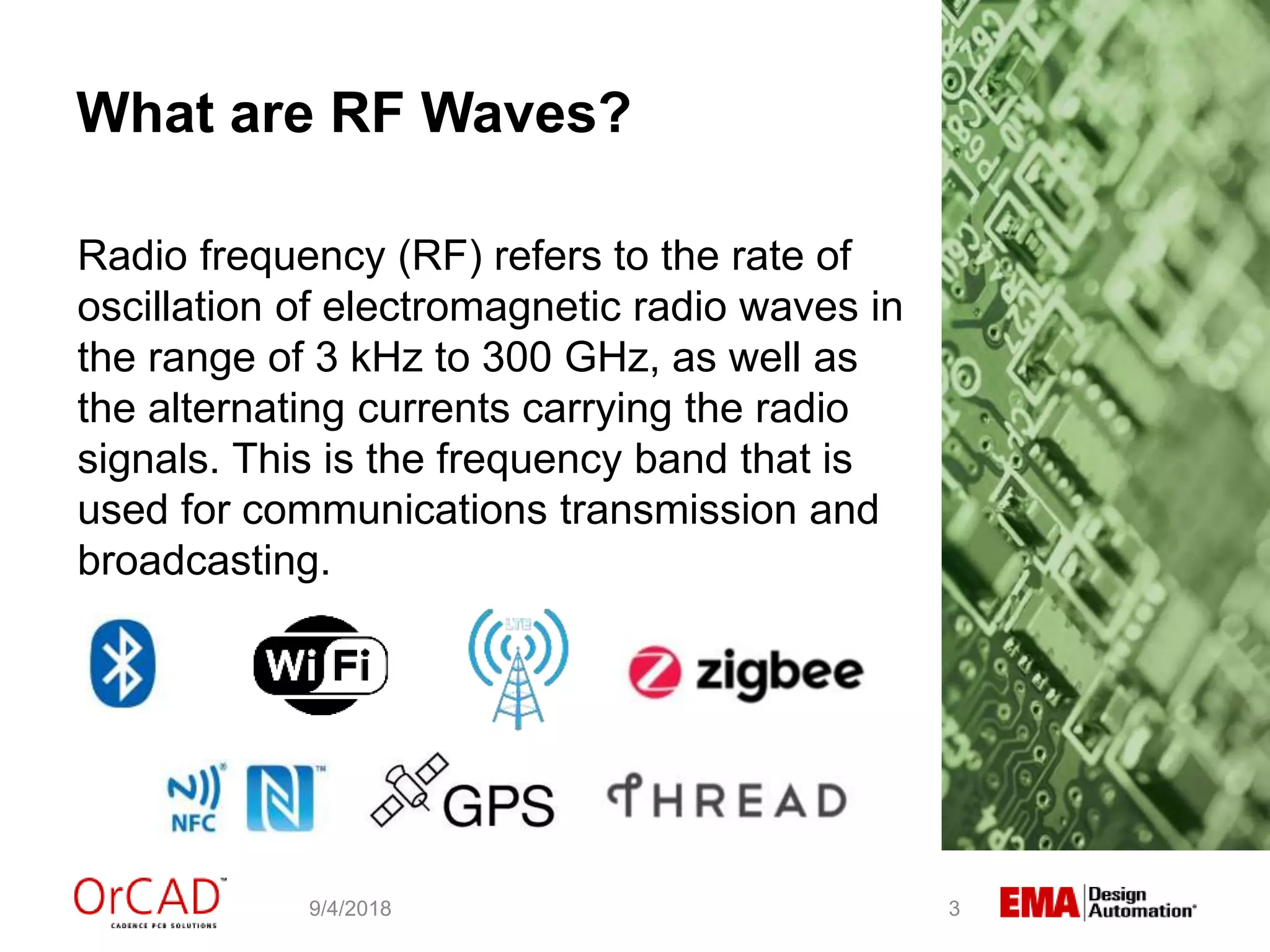
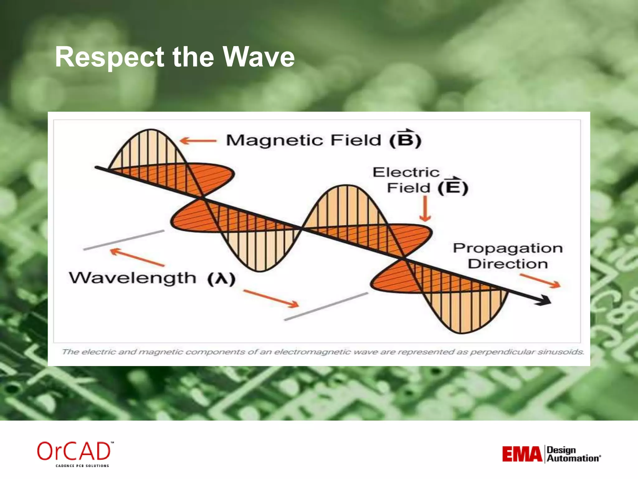
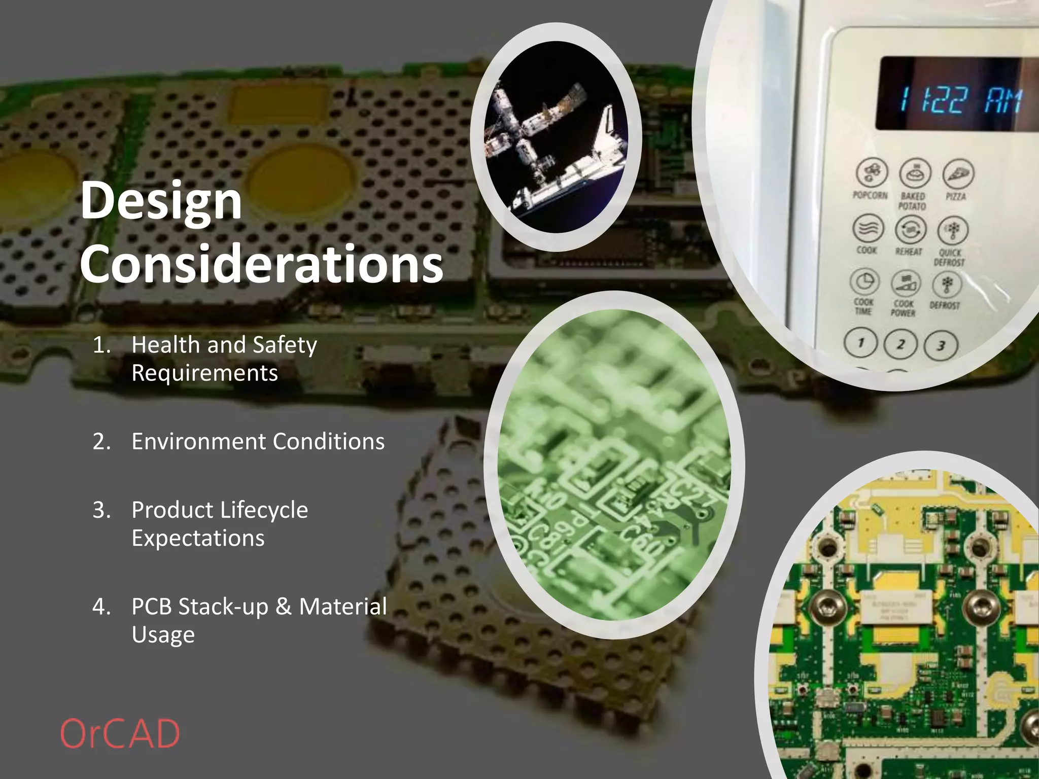
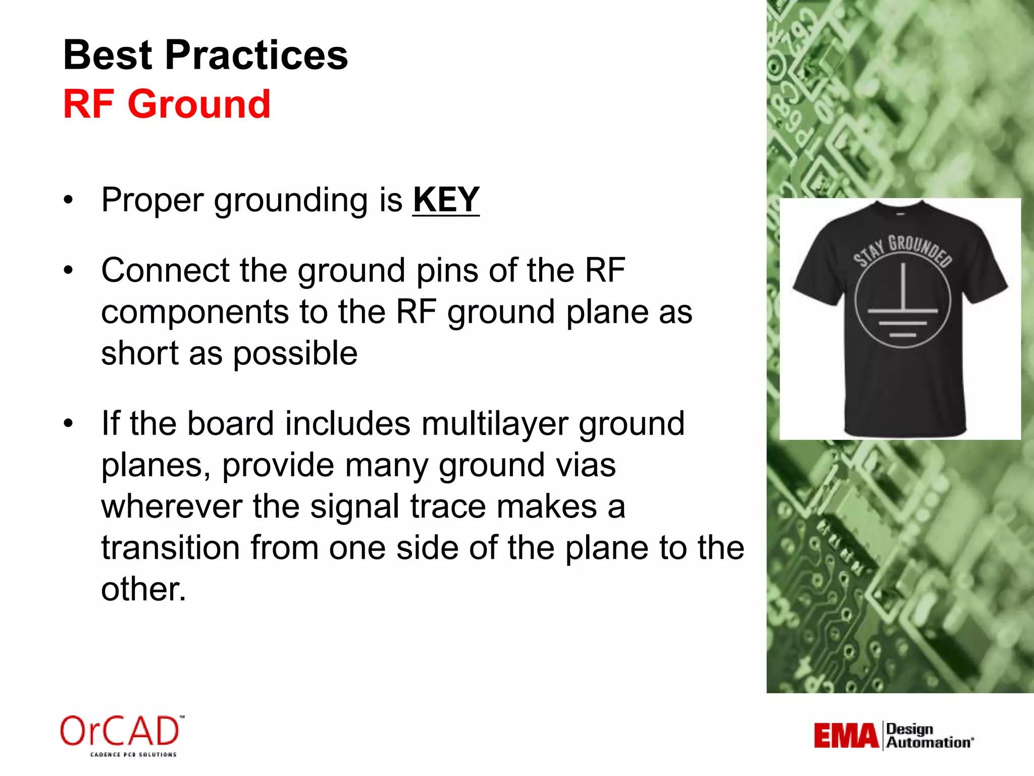
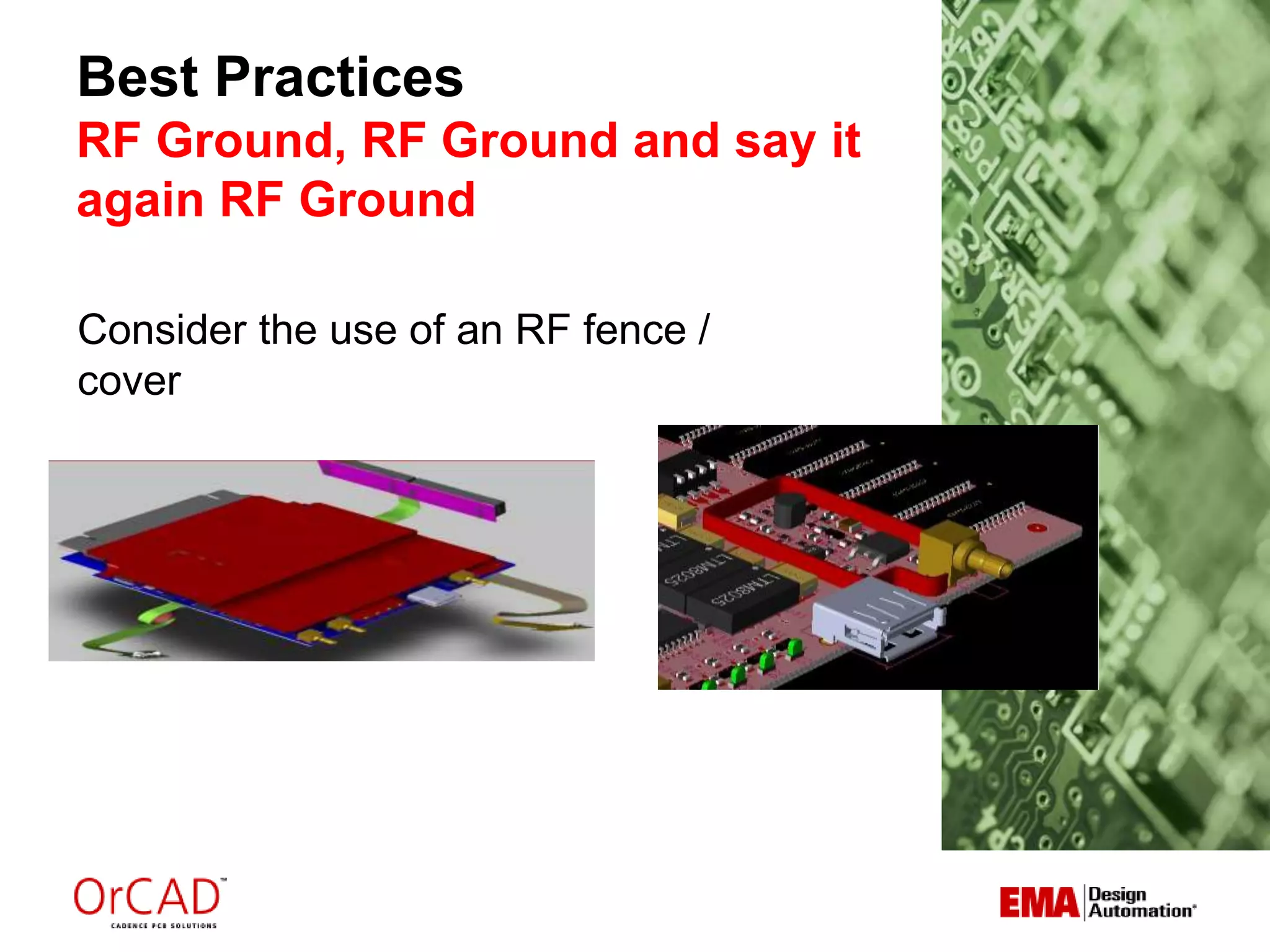
SlideShare a Scribd company logo
Orlen Bates
Sr. Application Engineer
RF Designs the Wave of the
Future
9/4/2018 1
Agenda
• What are RF Waves
• Design Considerations
• Best Practices
• Examples
• Q&A
9/4/2018 2
What are RF Waves?
Radio frequency (RF) refers to the rate of
oscillation of electromagnetic radio waves in
the range of 3 kHz to 300 GHz, as well as
the alternating currents carrying the radio
signals. This is the frequency band that is
used for communications transmission and
broadcasting.
9/4/2018 3
Respect the Wave
Design
Considerations
1. Health and Safety
Requirements
2. Environment Conditions
3. Product Lifecycle
Expectations
4. PCB Stack-up & Material
Usage
Best Practices
RF Ground
• Proper grounding is KEY
• Connect the ground pins of the RF
components to the RF ground plane as
short as possible
• If the board includes multilayer ground
planes, provide many ground vias
wherever the signal trace makes a
transition from one side of the plane to the
other.
Best Practices
RF Ground, RF Ground and say it
again RF Ground
Consider the use of an RF fence /
cover
Best Practices
Plating / Copper
• Use gold plating for RF components
created from etch
• No copper inlands near the RF circuitry
• No copper thieving near the RF circuitry
• Ground both ends of copper pours, and
stitch many vias wherever possible
• Separate RF planes from all other
planes
Best Practices
SMT vs. Thru Hole
• Use SMT parts for RF
• If thru-hole is required backdrilling should
be used with thru-hole components and
vias. This will remove that unwanted
antenna.
Best Practices
Stackup / Materials
• Multi-layer PCB is best
• Always provide continuous grounds
under traces
• Consider material selection carefully.
Standard FR4 may not meet your needs
Source: Isola
Best Practices
Vias
• Use isolated vias for separate portions of
a filter or matching network
• Use least number of vias in RF routing,
max number of vias in RF grounding
Best Practices
Routing
• Orient sensitive traces orthogonally
• Use short traces between the crystal and
RF device
• Keep interconnect traces separated as
much as possible
• Keep trace lengths to a minimum
Best Practices
Routing, Printed Circuit/Selection
• Adhere to proper corner routing
• Use wire-wound inductors whenever
possible and avoid using printed down
circuit parts unless needed
• Place inductors, coils and a planer
isolated from each other
Best Practices
Simulation
• Simulation is strongly recommended if
RF component is being printed / down as
part of the board
Key Takeaways
• Ground. Ground. Ground.
• Carefully consider RF implementation as
design choices will have a significant
impact on cost and complexity
• Understanding the effects RF circuitry
has on your design is half the battle…oh
and ground.
Demo
9/4/2018 Your PDN Gives Your Board Life 17
Thank you for joining us today.
Please contact us for more information on
OrCAD products, training, and services.
800-813-7494
info@ema-eda.com
www.ema-eda.com

More Related Content

Similar to Designing for RF - Tips and Tricks from the PCB Design Pros

Microstrip rectangular patch antenna
Microstrip rectangular  patch antennaMicrostrip rectangular  patch antenna
Microstrip rectangular patch antenna
charan -
 
Tranzeo%20 %20 Wireless%20 Isp%20 Primer
Tranzeo%20 %20 Wireless%20 Isp%20 PrimerTranzeo%20 %20 Wireless%20 Isp%20 Primer
Tranzeo%20 %20 Wireless%20 Isp%20 Primer
Shahab Shahid
 
AN102_ANTENNA_DESIGN_FEB_11.pdf
AN102_ANTENNA_DESIGN_FEB_11.pdfAN102_ANTENNA_DESIGN_FEB_11.pdf
AN102_ANTENNA_DESIGN_FEB_11.pdf
RAVIKUMAR Digital Signal Processing
 
Monopole
MonopoleMonopole
Monopole
c_archana
 
February 2014 column slideshare
February 2014 column slideshareFebruary 2014 column slideshare
February 2014 column slideshare
Sierra Circuits, Inc.
 
Rf microwave pc board deign and layout
Rf   microwave pc board deign and layoutRf   microwave pc board deign and layout
Rf microwave pc board deign and layout
锐澔 龙
 
MICROSTRIP ANTENNAS FOR RFID APPLICATION USING META-MATERIAL
MICROSTRIP ANTENNAS FOR RFID APPLICATION USING META-MATERIALMICROSTRIP ANTENNAS FOR RFID APPLICATION USING META-MATERIAL
MICROSTRIP ANTENNAS FOR RFID APPLICATION USING META-MATERIAL
NIKITA JANJAL
 
A complete guide for pcb 2.4G antenna design
A complete guide for pcb 2.4G antenna designA complete guide for pcb 2.4G antenna design
A complete guide for pcb 2.4G antenna design
Antenna Manufacturer Coco
 
Free space optical communication system
Free space optical communication systemFree space optical communication system
Free space optical communication system
Akshay Anand
 
IBS Training
IBS TrainingIBS Training
IBS Training
Tempus Telcosys
 
Copy of module 3.6-3.7.pptx
Copy of module 3.6-3.7.pptxCopy of module 3.6-3.7.pptx
Copy of module 3.6-3.7.pptx
MahadzirBinMatRabi
 
Pcb design powerpoint
Pcb design powerpointPcb design powerpoint
Pcb design powerpoint
Prashant329822
 
Pcbdesign 140510145153-phpapp01
Pcbdesign 140510145153-phpapp01Pcbdesign 140510145153-phpapp01
Pcbdesign 140510145153-phpapp01
ssantosh1234
 
FIBER OPTICS NETWORK DESIGN__.pptx
FIBER OPTICS NETWORK DESIGN__.pptxFIBER OPTICS NETWORK DESIGN__.pptx
FIBER OPTICS NETWORK DESIGN__.pptx
Sharathchandraprasad1
 
Novel Microstrip Antenna Design for UWB
Novel Microstrip Antenna Design for UWBNovel Microstrip Antenna Design for UWB
Novel Microstrip Antenna Design for UWB
Anas Kadri
 
IRJET- Design of Multiband Antenna for RF Energy Harvesting Circuits
IRJET- Design of Multiband Antenna for RF Energy Harvesting CircuitsIRJET- Design of Multiband Antenna for RF Energy Harvesting Circuits
IRJET- Design of Multiband Antenna for RF Energy Harvesting Circuits
IRJET Journal
 
Optical Fibre Network Design and Optical Noise
Optical Fibre Network Design and Optical NoiseOptical Fibre Network Design and Optical Noise
Optical Fibre Network Design and Optical Noise
Muzaffar Ali
 
PCB DESIGN - Introduction to PCB Design Manufacturing
PCB DESIGN - Introduction to PCB Design ManufacturingPCB DESIGN - Introduction to PCB Design Manufacturing
PCB DESIGN - Introduction to PCB Design Manufacturing
Vibrant Technologies & Computers
 
Microstrip patch antenna for wimax applications
Microstrip patch antenna for wimax applicationsMicrostrip patch antenna for wimax applications
Microstrip patch antenna for wimax applications
Abu Raneem
 
Analog Mixed-Signal Design in FinFET Processes
Analog Mixed-Signal Design in FinFET Processes Analog Mixed-Signal Design in FinFET Processes
Analog Mixed-Signal Design in FinFET Processes
Design World
 

Similar to Designing for RF - Tips and Tricks from the PCB Design Pros (20)

Microstrip rectangular patch antenna
Microstrip rectangular  patch antennaMicrostrip rectangular  patch antenna
Microstrip rectangular patch antenna
 
Tranzeo%20 %20 Wireless%20 Isp%20 Primer
Tranzeo%20 %20 Wireless%20 Isp%20 PrimerTranzeo%20 %20 Wireless%20 Isp%20 Primer
Tranzeo%20 %20 Wireless%20 Isp%20 Primer
 
AN102_ANTENNA_DESIGN_FEB_11.pdf
AN102_ANTENNA_DESIGN_FEB_11.pdfAN102_ANTENNA_DESIGN_FEB_11.pdf
AN102_ANTENNA_DESIGN_FEB_11.pdf
 
Monopole
MonopoleMonopole
Monopole
 
February 2014 column slideshare
February 2014 column slideshareFebruary 2014 column slideshare
February 2014 column slideshare
 
Rf microwave pc board deign and layout
Rf   microwave pc board deign and layoutRf   microwave pc board deign and layout
Rf microwave pc board deign and layout
 
MICROSTRIP ANTENNAS FOR RFID APPLICATION USING META-MATERIAL
MICROSTRIP ANTENNAS FOR RFID APPLICATION USING META-MATERIALMICROSTRIP ANTENNAS FOR RFID APPLICATION USING META-MATERIAL
MICROSTRIP ANTENNAS FOR RFID APPLICATION USING META-MATERIAL
 
A complete guide for pcb 2.4G antenna design
A complete guide for pcb 2.4G antenna designA complete guide for pcb 2.4G antenna design
A complete guide for pcb 2.4G antenna design
 
Free space optical communication system
Free space optical communication systemFree space optical communication system
Free space optical communication system
 
IBS Training
IBS TrainingIBS Training
IBS Training
 
Copy of module 3.6-3.7.pptx
Copy of module 3.6-3.7.pptxCopy of module 3.6-3.7.pptx
Copy of module 3.6-3.7.pptx
 
Pcb design powerpoint
Pcb design powerpointPcb design powerpoint
Pcb design powerpoint
 
Pcbdesign 140510145153-phpapp01
Pcbdesign 140510145153-phpapp01Pcbdesign 140510145153-phpapp01
Pcbdesign 140510145153-phpapp01
 
FIBER OPTICS NETWORK DESIGN__.pptx
FIBER OPTICS NETWORK DESIGN__.pptxFIBER OPTICS NETWORK DESIGN__.pptx
FIBER OPTICS NETWORK DESIGN__.pptx
 
Novel Microstrip Antenna Design for UWB
Novel Microstrip Antenna Design for UWBNovel Microstrip Antenna Design for UWB
Novel Microstrip Antenna Design for UWB
 
IRJET- Design of Multiband Antenna for RF Energy Harvesting Circuits
IRJET- Design of Multiband Antenna for RF Energy Harvesting CircuitsIRJET- Design of Multiband Antenna for RF Energy Harvesting Circuits
IRJET- Design of Multiband Antenna for RF Energy Harvesting Circuits
 
Optical Fibre Network Design and Optical Noise
Optical Fibre Network Design and Optical NoiseOptical Fibre Network Design and Optical Noise
Optical Fibre Network Design and Optical Noise
 
PCB DESIGN - Introduction to PCB Design Manufacturing
PCB DESIGN - Introduction to PCB Design ManufacturingPCB DESIGN - Introduction to PCB Design Manufacturing
PCB DESIGN - Introduction to PCB Design Manufacturing
 
Microstrip patch antenna for wimax applications
Microstrip patch antenna for wimax applicationsMicrostrip patch antenna for wimax applications
Microstrip patch antenna for wimax applications
 
Analog Mixed-Signal Design in FinFET Processes
Analog Mixed-Signal Design in FinFET Processes Analog Mixed-Signal Design in FinFET Processes
Analog Mixed-Signal Design in FinFET Processes
 

More from EMA Design Automation

Serial Link Design - Meeting the Need for Speed
Serial Link Design - Meeting the Need for SpeedSerial Link Design - Meeting the Need for Speed
Serial Link Design - Meeting the Need for Speed
EMA Design Automation
 
Power Supply Webinar
Power Supply WebinarPower Supply Webinar
Power Supply Webinar
EMA Design Automation
 
Design for Manufacturing (DFM) and Why it Matters
Design for Manufacturing (DFM) and Why it MattersDesign for Manufacturing (DFM) and Why it Matters
Design for Manufacturing (DFM) and Why it Matters
EMA Design Automation
 
Your PCB Power Delivery Network (PDN) Gives Your Board Life
Your PCB Power Delivery Network (PDN) Gives Your Board LifeYour PCB Power Delivery Network (PDN) Gives Your Board Life
Your PCB Power Delivery Network (PDN) Gives Your Board Life
EMA Design Automation
 
What's New - OrCAD 17.2 QIR 6
What's New - OrCAD 17.2 QIR 6What's New - OrCAD 17.2 QIR 6
What's New - OrCAD 17.2 QIR 6
EMA Design Automation
 
PCB Data Management Webinar
PCB Data Management WebinarPCB Data Management Webinar
PCB Data Management Webinar
EMA Design Automation
 
PCB Virtual Prototyping with PSpice
PCB Virtual Prototyping with PSpicePCB Virtual Prototyping with PSpice
PCB Virtual Prototyping with PSpice
EMA Design Automation
 
Modeling an Embedded Device for PSpice Simulation
Modeling an Embedded Device for PSpice SimulationModeling an Embedded Device for PSpice Simulation
Modeling an Embedded Device for PSpice Simulation
EMA Design Automation
 
PTC Live: Integrating PTC Windchill with Cadence PCB Design
PTC Live: Integrating PTC Windchill with Cadence PCB DesignPTC Live: Integrating PTC Windchill with Cadence PCB Design
PTC Live: Integrating PTC Windchill with Cadence PCB Design
EMA Design Automation
 
OrCAD Panel Editor
OrCAD Panel EditorOrCAD Panel Editor
OrCAD Panel Editor
EMA Design Automation
 
Implementing a Flexible Design Reuse Methodology
Implementing a Flexible Design Reuse MethodologyImplementing a Flexible Design Reuse Methodology
Implementing a Flexible Design Reuse Methodology
EMA Design Automation
 
OrCAD Constraint Driven Design Flow
OrCAD Constraint Driven Design FlowOrCAD Constraint Driven Design Flow
OrCAD Constraint Driven Design Flow
EMA Design Automation
 
ECAD MCAD Design Data Management with PTC Windchill and Cadence Allegro PCB
ECAD MCAD Design Data Management with PTC Windchill and Cadence Allegro PCBECAD MCAD Design Data Management with PTC Windchill and Cadence Allegro PCB
ECAD MCAD Design Data Management with PTC Windchill and Cadence Allegro PCB
EMA Design Automation
 
OrCAD Library Builder Overview Presentation
OrCAD Library Builder Overview PresentationOrCAD Library Builder Overview Presentation
OrCAD Library Builder Overview Presentation
EMA Design Automation
 
OrCAD Documentation Editor PCB Documentation Environment
OrCAD Documentation Editor PCB Documentation EnvironmentOrCAD Documentation Editor PCB Documentation Environment
OrCAD Documentation Editor PCB Documentation Environment
EMA Design Automation
 
PCB Design and Data Management
PCB Design and Data ManagementPCB Design and Data Management
PCB Design and Data Management
EMA Design Automation
 
Implementing Electrical and Simulation Rule Checks to ensure Signal Quality
Implementing Electrical and Simulation Rule Checks to ensure Signal QualityImplementing Electrical and Simulation Rule Checks to ensure Signal Quality
Implementing Electrical and Simulation Rule Checks to ensure Signal Quality
EMA Design Automation
 
Analog Mixed Signal Simulation With PSpice
Analog Mixed Signal Simulation With PSpiceAnalog Mixed Signal Simulation With PSpice
Analog Mixed Signal Simulation With PSpice
EMA Design Automation
 

More from EMA Design Automation (18)

Serial Link Design - Meeting the Need for Speed
Serial Link Design - Meeting the Need for SpeedSerial Link Design - Meeting the Need for Speed
Serial Link Design - Meeting the Need for Speed
 
Power Supply Webinar
Power Supply WebinarPower Supply Webinar
Power Supply Webinar
 
Design for Manufacturing (DFM) and Why it Matters
Design for Manufacturing (DFM) and Why it MattersDesign for Manufacturing (DFM) and Why it Matters
Design for Manufacturing (DFM) and Why it Matters
 
Your PCB Power Delivery Network (PDN) Gives Your Board Life
Your PCB Power Delivery Network (PDN) Gives Your Board LifeYour PCB Power Delivery Network (PDN) Gives Your Board Life
Your PCB Power Delivery Network (PDN) Gives Your Board Life
 
What's New - OrCAD 17.2 QIR 6
What's New - OrCAD 17.2 QIR 6What's New - OrCAD 17.2 QIR 6
What's New - OrCAD 17.2 QIR 6
 
PCB Data Management Webinar
PCB Data Management WebinarPCB Data Management Webinar
PCB Data Management Webinar
 
PCB Virtual Prototyping with PSpice
PCB Virtual Prototyping with PSpicePCB Virtual Prototyping with PSpice
PCB Virtual Prototyping with PSpice
 
Modeling an Embedded Device for PSpice Simulation
Modeling an Embedded Device for PSpice SimulationModeling an Embedded Device for PSpice Simulation
Modeling an Embedded Device for PSpice Simulation
 
PTC Live: Integrating PTC Windchill with Cadence PCB Design
PTC Live: Integrating PTC Windchill with Cadence PCB DesignPTC Live: Integrating PTC Windchill with Cadence PCB Design
PTC Live: Integrating PTC Windchill with Cadence PCB Design
 
OrCAD Panel Editor
OrCAD Panel EditorOrCAD Panel Editor
OrCAD Panel Editor
 
Implementing a Flexible Design Reuse Methodology
Implementing a Flexible Design Reuse MethodologyImplementing a Flexible Design Reuse Methodology
Implementing a Flexible Design Reuse Methodology
 
OrCAD Constraint Driven Design Flow
OrCAD Constraint Driven Design FlowOrCAD Constraint Driven Design Flow
OrCAD Constraint Driven Design Flow
 
ECAD MCAD Design Data Management with PTC Windchill and Cadence Allegro PCB
ECAD MCAD Design Data Management with PTC Windchill and Cadence Allegro PCBECAD MCAD Design Data Management with PTC Windchill and Cadence Allegro PCB
ECAD MCAD Design Data Management with PTC Windchill and Cadence Allegro PCB
 
OrCAD Library Builder Overview Presentation
OrCAD Library Builder Overview PresentationOrCAD Library Builder Overview Presentation
OrCAD Library Builder Overview Presentation
 
OrCAD Documentation Editor PCB Documentation Environment
OrCAD Documentation Editor PCB Documentation EnvironmentOrCAD Documentation Editor PCB Documentation Environment
OrCAD Documentation Editor PCB Documentation Environment
 
PCB Design and Data Management
PCB Design and Data ManagementPCB Design and Data Management
PCB Design and Data Management
 
Implementing Electrical and Simulation Rule Checks to ensure Signal Quality
Implementing Electrical and Simulation Rule Checks to ensure Signal QualityImplementing Electrical and Simulation Rule Checks to ensure Signal Quality
Implementing Electrical and Simulation Rule Checks to ensure Signal Quality
 
Analog Mixed Signal Simulation With PSpice
Analog Mixed Signal Simulation With PSpiceAnalog Mixed Signal Simulation With PSpice
Analog Mixed Signal Simulation With PSpice
 

Recently uploaded

basic-wireline-operations-course-mahmoud-f-radwan.pdf
basic-wireline-operations-course-mahmoud-f-radwan.pdfbasic-wireline-operations-course-mahmoud-f-radwan.pdf
basic-wireline-operations-course-mahmoud-f-radwan.pdf
NidhalKahouli2
 
International Conference on NLP, Artificial Intelligence, Machine Learning an...
International Conference on NLP, Artificial Intelligence, Machine Learning an...International Conference on NLP, Artificial Intelligence, Machine Learning an...
International Conference on NLP, Artificial Intelligence, Machine Learning an...
gerogepatton
 
New techniques for characterising damage in rock slopes.pdf
New techniques for characterising damage in rock slopes.pdfNew techniques for characterising damage in rock slopes.pdf
New techniques for characterising damage in rock slopes.pdf
wisnuprabawa3
 
CSM Cloud Service Management Presentarion
CSM Cloud Service Management PresentarionCSM Cloud Service Management Presentarion
CSM Cloud Service Management Presentarion
rpskprasana
 
Computational Engineering IITH Presentation
Computational Engineering IITH PresentationComputational Engineering IITH Presentation
Computational Engineering IITH Presentation
co23btech11018
 
ACEP Magazine edition 4th launched on 05.06.2024
ACEP Magazine edition 4th launched on 05.06.2024ACEP Magazine edition 4th launched on 05.06.2024
ACEP Magazine edition 4th launched on 05.06.2024
Rahul
 
Generative AI leverages algorithms to create various forms of content
Generative AI leverages algorithms to create various forms of contentGenerative AI leverages algorithms to create various forms of content
Generative AI leverages algorithms to create various forms of content
Hitesh Mohapatra
 
A review on techniques and modelling methodologies used for checking electrom...
A review on techniques and modelling methodologies used for checking electrom...A review on techniques and modelling methodologies used for checking electrom...
A review on techniques and modelling methodologies used for checking electrom...
nooriasukmaningtyas
 
5214-1693458878915-Unit 6 2023 to 2024 academic year assignment (AutoRecovere...
5214-1693458878915-Unit 6 2023 to 2024 academic year assignment (AutoRecovere...5214-1693458878915-Unit 6 2023 to 2024 academic year assignment (AutoRecovere...
5214-1693458878915-Unit 6 2023 to 2024 academic year assignment (AutoRecovere...
ihlasbinance2003
 
KuberTENes Birthday Bash Guadalajara - K8sGPT first impressions
KuberTENes Birthday Bash Guadalajara - K8sGPT first impressionsKuberTENes Birthday Bash Guadalajara - K8sGPT first impressions
KuberTENes Birthday Bash Guadalajara - K8sGPT first impressions
Victor Morales
 
Understanding Inductive Bias in Machine Learning
Understanding Inductive Bias in Machine LearningUnderstanding Inductive Bias in Machine Learning
Understanding Inductive Bias in Machine Learning
SUTEJAS
 
ISPM 15 Heat Treated Wood Stamps and why your shipping must have one
ISPM 15 Heat Treated Wood Stamps and why your shipping must have oneISPM 15 Heat Treated Wood Stamps and why your shipping must have one
ISPM 15 Heat Treated Wood Stamps and why your shipping must have one
Las Vegas Warehouse
 
Literature Review Basics and Understanding Reference Management.pptx
Literature Review Basics and Understanding Reference Management.pptxLiterature Review Basics and Understanding Reference Management.pptx
Literature Review Basics and Understanding Reference Management.pptx
Dr Ramhari Poudyal
 
22CYT12-Unit-V-E Waste and its Management.ppt
22CYT12-Unit-V-E Waste and its Management.ppt22CYT12-Unit-V-E Waste and its Management.ppt
22CYT12-Unit-V-E Waste and its Management.ppt
KrishnaveniKrishnara1
 
Heat Resistant Concrete Presentation ppt
Heat Resistant Concrete Presentation pptHeat Resistant Concrete Presentation ppt
Heat Resistant Concrete Presentation ppt
mamunhossenbd75
 
Engine Lubrication performance System.pdf
Engine Lubrication performance System.pdfEngine Lubrication performance System.pdf
Engine Lubrication performance System.pdf
mamamaam477
 
Modelagem de um CSTR com reação endotermica.pdf
Modelagem de um CSTR com reação endotermica.pdfModelagem de um CSTR com reação endotermica.pdf
Modelagem de um CSTR com reação endotermica.pdf
camseq
 
Presentation of IEEE Slovenia CIS (Computational Intelligence Society) Chapte...
Presentation of IEEE Slovenia CIS (Computational Intelligence Society) Chapte...Presentation of IEEE Slovenia CIS (Computational Intelligence Society) Chapte...
Presentation of IEEE Slovenia CIS (Computational Intelligence Society) Chapte...
University of Maribor
 
Textile Chemical Processing and Dyeing.pdf
Textile Chemical Processing and Dyeing.pdfTextile Chemical Processing and Dyeing.pdf
Textile Chemical Processing and Dyeing.pdf
NazakatAliKhoso2
 
ML Based Model for NIDS MSc Updated Presentation.v2.pptx
ML Based Model for NIDS MSc Updated Presentation.v2.pptxML Based Model for NIDS MSc Updated Presentation.v2.pptx
ML Based Model for NIDS MSc Updated Presentation.v2.pptx
JamalHussainArman
 

Recently uploaded (20)

basic-wireline-operations-course-mahmoud-f-radwan.pdf
basic-wireline-operations-course-mahmoud-f-radwan.pdfbasic-wireline-operations-course-mahmoud-f-radwan.pdf
basic-wireline-operations-course-mahmoud-f-radwan.pdf
 
International Conference on NLP, Artificial Intelligence, Machine Learning an...
International Conference on NLP, Artificial Intelligence, Machine Learning an...International Conference on NLP, Artificial Intelligence, Machine Learning an...
International Conference on NLP, Artificial Intelligence, Machine Learning an...
 
New techniques for characterising damage in rock slopes.pdf
New techniques for characterising damage in rock slopes.pdfNew techniques for characterising damage in rock slopes.pdf
New techniques for characterising damage in rock slopes.pdf
 
CSM Cloud Service Management Presentarion
CSM Cloud Service Management PresentarionCSM Cloud Service Management Presentarion
CSM Cloud Service Management Presentarion
 
Computational Engineering IITH Presentation
Computational Engineering IITH PresentationComputational Engineering IITH Presentation
Computational Engineering IITH Presentation
 
ACEP Magazine edition 4th launched on 05.06.2024
ACEP Magazine edition 4th launched on 05.06.2024ACEP Magazine edition 4th launched on 05.06.2024
ACEP Magazine edition 4th launched on 05.06.2024
 
Generative AI leverages algorithms to create various forms of content
Generative AI leverages algorithms to create various forms of contentGenerative AI leverages algorithms to create various forms of content
Generative AI leverages algorithms to create various forms of content
 
A review on techniques and modelling methodologies used for checking electrom...
A review on techniques and modelling methodologies used for checking electrom...A review on techniques and modelling methodologies used for checking electrom...
A review on techniques and modelling methodologies used for checking electrom...
 
5214-1693458878915-Unit 6 2023 to 2024 academic year assignment (AutoRecovere...
5214-1693458878915-Unit 6 2023 to 2024 academic year assignment (AutoRecovere...5214-1693458878915-Unit 6 2023 to 2024 academic year assignment (AutoRecovere...
5214-1693458878915-Unit 6 2023 to 2024 academic year assignment (AutoRecovere...
 
KuberTENes Birthday Bash Guadalajara - K8sGPT first impressions
KuberTENes Birthday Bash Guadalajara - K8sGPT first impressionsKuberTENes Birthday Bash Guadalajara - K8sGPT first impressions
KuberTENes Birthday Bash Guadalajara - K8sGPT first impressions
 
Understanding Inductive Bias in Machine Learning
Understanding Inductive Bias in Machine LearningUnderstanding Inductive Bias in Machine Learning
Understanding Inductive Bias in Machine Learning
 
ISPM 15 Heat Treated Wood Stamps and why your shipping must have one
ISPM 15 Heat Treated Wood Stamps and why your shipping must have oneISPM 15 Heat Treated Wood Stamps and why your shipping must have one
ISPM 15 Heat Treated Wood Stamps and why your shipping must have one
 
Literature Review Basics and Understanding Reference Management.pptx
Literature Review Basics and Understanding Reference Management.pptxLiterature Review Basics and Understanding Reference Management.pptx
Literature Review Basics and Understanding Reference Management.pptx
 
22CYT12-Unit-V-E Waste and its Management.ppt
22CYT12-Unit-V-E Waste and its Management.ppt22CYT12-Unit-V-E Waste and its Management.ppt
22CYT12-Unit-V-E Waste and its Management.ppt
 
Heat Resistant Concrete Presentation ppt
Heat Resistant Concrete Presentation pptHeat Resistant Concrete Presentation ppt
Heat Resistant Concrete Presentation ppt
 
Engine Lubrication performance System.pdf
Engine Lubrication performance System.pdfEngine Lubrication performance System.pdf
Engine Lubrication performance System.pdf
 
Modelagem de um CSTR com reação endotermica.pdf
Modelagem de um CSTR com reação endotermica.pdfModelagem de um CSTR com reação endotermica.pdf
Modelagem de um CSTR com reação endotermica.pdf
 
Presentation of IEEE Slovenia CIS (Computational Intelligence Society) Chapte...
Presentation of IEEE Slovenia CIS (Computational Intelligence Society) Chapte...Presentation of IEEE Slovenia CIS (Computational Intelligence Society) Chapte...
Presentation of IEEE Slovenia CIS (Computational Intelligence Society) Chapte...
 
Textile Chemical Processing and Dyeing.pdf
Textile Chemical Processing and Dyeing.pdfTextile Chemical Processing and Dyeing.pdf
Textile Chemical Processing and Dyeing.pdf
 
ML Based Model for NIDS MSc Updated Presentation.v2.pptx
ML Based Model for NIDS MSc Updated Presentation.v2.pptxML Based Model for NIDS MSc Updated Presentation.v2.pptx
ML Based Model for NIDS MSc Updated Presentation.v2.pptx
 

Designing for RF - Tips and Tricks from the PCB Design Pros

  • 1. Orlen Bates Sr. Application Engineer RF Designs the Wave of the Future 9/4/2018 1
  • 2. Agenda • What are RF Waves • Design Considerations • Best Practices • Examples • Q&A 9/4/2018 2
  • 3. What are RF Waves? Radio frequency (RF) refers to the rate of oscillation of electromagnetic radio waves in the range of 3 kHz to 300 GHz, as well as the alternating currents carrying the radio signals. This is the frequency band that is used for communications transmission and broadcasting. 9/4/2018 3
  • 5. Design Considerations 1. Health and Safety Requirements 2. Environment Conditions 3. Product Lifecycle Expectations 4. PCB Stack-up & Material Usage
  • 6. Best Practices RF Ground • Proper grounding is KEY • Connect the ground pins of the RF components to the RF ground plane as short as possible • If the board includes multilayer ground planes, provide many ground vias wherever the signal trace makes a transition from one side of the plane to the other.
  • 7. Best Practices RF Ground, RF Ground and say it again RF Ground Consider the use of an RF fence / cover
  • 8. Best Practices Plating / Copper • Use gold plating for RF components created from etch • No copper inlands near the RF circuitry • No copper thieving near the RF circuitry • Ground both ends of copper pours, and stitch many vias wherever possible • Separate RF planes from all other planes
  • 9. Best Practices SMT vs. Thru Hole • Use SMT parts for RF • If thru-hole is required backdrilling should be used with thru-hole components and vias. This will remove that unwanted antenna.
  • 10. Best Practices Stackup / Materials • Multi-layer PCB is best • Always provide continuous grounds under traces • Consider material selection carefully. Standard FR4 may not meet your needs Source: Isola
  • 11. Best Practices Vias • Use isolated vias for separate portions of a filter or matching network • Use least number of vias in RF routing, max number of vias in RF grounding
  • 12. Best Practices Routing • Orient sensitive traces orthogonally • Use short traces between the crystal and RF device • Keep interconnect traces separated as much as possible • Keep trace lengths to a minimum
  • 13. Best Practices Routing, Printed Circuit/Selection • Adhere to proper corner routing • Use wire-wound inductors whenever possible and avoid using printed down circuit parts unless needed • Place inductors, coils and a planer isolated from each other
  • 14. Best Practices Simulation • Simulation is strongly recommended if RF component is being printed / down as part of the board
  • 15. Key Takeaways • Ground. Ground. Ground. • Carefully consider RF implementation as design choices will have a significant impact on cost and complexity • Understanding the effects RF circuitry has on your design is half the battle…oh and ground.
  • 16. Demo
  • 17. 9/4/2018 Your PDN Gives Your Board Life 17 Thank you for joining us today. Please contact us for more information on OrCAD products, training, and services. 800-813-7494 info@ema-eda.com www.ema-eda.com

Editor's Notes

  1. My first RF design was with hand taping and an x-acto knife, trimming the bishop graphic tape ordering boards, re-trimming the tape and respinning over and over until we got it correct. I remember the EE saying “RF Design the Wave of the Future”. I believe the future is here, with Wi-Fi needed for just about everything we design.
  2. The term microwave is a reference to a class of waves, referenced as a microwave range or spectrum of frequencies that the Wi-Fi signal operates. For Example, the Wi-Fi signal from your laptop is often transmitted at 2.4 GHz, a frequency found within the microwave range, or spectrum of 300 MHz to 300 GHz the same frequency as our microwave ovens. The wavelength of an alternating current depends on the frequency.
  3. The distance between Wi-Fi waves is shorter than that of radio waves but longer than that of microwaves, giving Wi-Fi a unique transmission band that can’t be interrupted by other signals. Wi-Fi waves are about 3 to 5 inches from crest to crest show here in the Wavelength measurement. So, the main difference between radio waves and microwaves is its wavelength and frequency operation. The only difference is the wavelength of the propagation or radiation. Various portions of the electromagnetic spectrum are reserved for specific uses, like radio, short wave radio, television, garage door openers, etc. One example is my garage door opener, half way down my driveway I can open one of the three doors, so all three doors has a different frequency. But as months go by I have to move closer to the garage door to open it. So why is that? The electric field is getting weak, how do I fix that? New battery in the remote. The garage door company I went with has the frequency rotating so it not the same each time, keeping us safe.
  4. Rf energy in medical treatments has been used for over 75 years. MRI uses RF waves to generate images of the human body. Cauterize of the blood vessels in surgery for year now.
  5. Vias in the ground pads are the best, we call that via-in-pad. Vias in a signal pad is best if the need is to change layers.
  6. Shielding is what it is all about.
  7. Soldermask removed from the RF traces so by having no soldermask where the RF fields are, gives the best transmission and if your board is made by different fabs, you get the most repeatable transmission.
  8. Stubs on the vias and thru hole padstacks are just as bad as the copper thieving or copper inlands we had just talked about. They become unwanted antennas.
  9. FR4 might be cheaper material but to respect the wave and its requirements, FR4 can fail in some applications.
  10. Via for shielding, is a number one requirement.
  11. If inductors, planar, coils are created as copper parts grounding and shielding for isolation is a must.
  12. Any serious RF designs should be simulated, we interface with IFF files and DXF files.
  13. The real issues will start when your RF circuit needs to be added to the digital design. They do not get along grounding is your best defense in this battle.