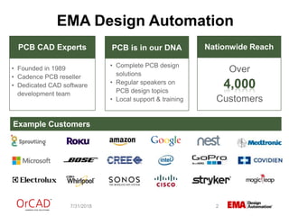
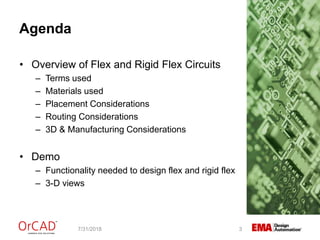
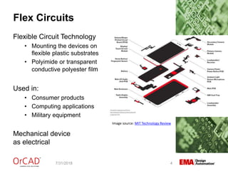
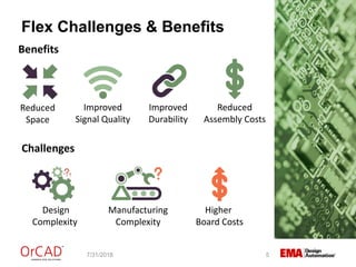
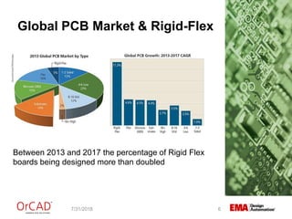
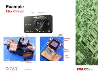
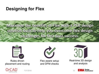
Let’s Get FLEXible Webinar
7/31/2018 1
Presented By: Janine Flagg
Field Applications Engineer
eMail: janinef@ema-eda.com
PCB CAD Experts Nationwide Reach
Over
4,000
Customers
Example Customers
PCB is in our DNA
EMA Design Automation
• Complete PCB design
solutions
• Regular speakers on
PCB design topics
• Local support & training
• Founded in 1989
• Cadence PCB reseller
• Dedicated CAD software
development team
7/31/2018 2
Agenda
• Overview of Flex and Rigid Flex Circuits
– Terms used
– Materials used
– Placement Considerations
– Routing Considerations
– 3D & Manufacturing Considerations
• Demo
– Functionality needed to design flex and rigid flex
– 3-D views
7/31/2018 3
Flex Circuits
7/31/2018 4
Flexible Circuit Technology
• Mounting the devices on
flexible plastic substrates
• Polyimide or transparent
conductive polyester film
Used in:
• Consumer products
• Computing applications
• Military equipment
Mechanical device
as electrical
Image source: MIT Technology Review
Flex Challenges & Benefits
7/31/2018 5
Reduced
Space
Improved
Signal Quality
Improved
Durability
Reduced
Assembly Costs
Benefits
Challenges
Design
Complexity
Manufacturing
Complexity
Higher
Board Costs
Global PCB Market & Rigid-Flex
7/31/2018 6
Between 2013 and 2017 the percentage of Rigid Flex
boards being designed more than doubled
Example
Flex Circuit
7/31/2018 7
Example
Rigid Flex
7/31/2018 8
Types of Flex Circuits
Single layer
• Mounted on single conductor layer
• Metal or conductive polymer, over a
flexible dielectric film
Double layer
• Placed on two conductor layers
Multi layer
• Span three or more layers
• May not be continuously laminated
• May have openings
7/31/2018 10
Rigid-Flex Circuits
• Flex circuits placed on
rigid substrates
• Flex circuits placed on
flexible substrates
• Laminated together into
a single structure
7/31/2018 11
Flex Circuit Terms
Coverlay
7/31/2018 12
• Used to encapsulate and protect the
external circuitry
• Serves the same function as
soldermask on a rigid PCB
• Differences:
– Flexibility
– Durability
• Typical coverlay thickness:
– 0.001” polyimide
– 0.001” adhesive
Flex Circuit Terms
Stiffener
7/31/2018 13
Used to:
– Reinforce areas of flexible circuitry
– Component support,
– Durability and mounting
Can also be used for:
– Strain relief
– Heat dissipation
Bonding materials include:
– Pressure Sensitive Adhesive (PSA)
– Temperature Sensitive Adhesive (TSA)
Stiffener Materials:
– Unclad FR4 / G10
– Polyimide
Flex Circuit Terms
Bend Area
7/31/2018 14
• An area on the board
where a bend may occur
• Define Areas
– Width
– Radius
• Bend Area
– Via Keepout
– Package Keepout
Bend Line
Flex Area
Bend Area
Flex Circuit Terms
Materials
7/31/2018 15
• Wide variety of materials
– Films
– Foils
– Adhesives
– Polyester
– Polyimide
• Choice depends on how
and where the circuit will
be assembled and used
• Consultation of fabricator
is required
• Cross-section setup per
design requirements
• Not all layers exist in all
zones
• Care must be taken during
placement and routing to
ensure you are referencing
the desired layers
Design Considerations
Layer Structures
7/31/2018 16
Design Considerations
Routing in Flex Regions
7/31/2018 18
• Rigid-flex designs require curved
bus lines
• Routes to follow contour of flex
area
• Arc corners should be used
whenever possible (especially in
bend areas)
• Flex board outlines often change
during design cycle. Ability to
quick adjust routes is key to
efficiency
Design Considerations
Placement & Routing in Bend Areas
7/31/2018 19
• Care must be taken when
working in or around bend areas
• Traces must cross bend areas
perpendicularly to minimize
material stress
• Adjacent layer routing through
the bend area should be offset to
prevent what is called the I-
BEAM effect
• Pins and vias should not be
allowed within or near bend
areas to prevent cracking
Design Considerations
Conductor and Pad Design
7/31/2018 21
• Pads should have tie downs
(also called anchoring spurs
or rabbit ears) to prevent
separation between the
copper and the base
material
• All pads should be filleted
because they reduce stress
points. This helps eliminate
breaking during flexing
Design Considerations
Shielding
7/31/2018 22
• Required to block unwanted
electronic interference
• Ground areas of flex circuits
should be crosshatched
• Helps
– Reduce weight
– Improve circuit flexibility
– Prevent tearing
Design Considerations
MCAD Communication
7/31/2018 23
• Often bend areas and flex radius will
be defined by mechanical
requirements
• It is important to maintain close
communication with MCAD for any
design changes
• Bi-directional data sharing of flex
info (bend, layer structure, etc) is
critical between CAD systems
Design Considerations
Fit and Clearance
7/31/2018 24
• Must analyze flex for fit in 3D
• Ideally this can be done by the
PCB designer
• Checking should be done not
only at completed bend state but
during bend as well
Design Considerations
DFM & Manufacturer Handoff
7/31/2018 25
• Flex designs require additional checking and
review
• Flex regions will have specific requirements
that differ from rigid sections including:
– Soldermask to Stiffener
– Coverlay to Soldermask
– Silkscreen to bend region
– Stiffener to via, outline, bend
– Etc
• Using a intelligent interchange format like
IPC-2581 will help your manufacturer capture
your design intent
• Engage with your manufacturer early and
often as need
Demo Time!
7/31/2018 32
Designing for Flex
7/31/2018 33
Maximize the benefits of Flex with a PCB design
solution built to help you overcome flex design
challenges for first pass success.
Rules driven
placement and routing
Flex aware setup
and DFM checks
Real-time 3D design
and analysis
7/31/2018 Why DFM Matters 34
Thank you for joining us today.
Please contact us for more information on
OrCAD products, training, and services.
800-813-7494
info@ema-eda.com
www.ema-eda.com
Up next:
Designing for Power Integrity (PI)
Learn how to ensure a healthy PDN and your
keep products humming smoothly.

Let's Get Flexible: Expert Tips for Designing Flex PCBs

  • 1.
    Let’s Get FLEXibleWebinar 7/31/2018 1 Presented By: Janine Flagg Field Applications Engineer eMail: janinef@ema-eda.com
  • 2.
    PCB CAD ExpertsNationwide Reach Over 4,000 Customers Example Customers PCB is in our DNA EMA Design Automation • Complete PCB design solutions • Regular speakers on PCB design topics • Local support & training • Founded in 1989 • Cadence PCB reseller • Dedicated CAD software development team 7/31/2018 2
  • 3.
    Agenda • Overview ofFlex and Rigid Flex Circuits – Terms used – Materials used – Placement Considerations – Routing Considerations – 3D & Manufacturing Considerations • Demo – Functionality needed to design flex and rigid flex – 3-D views 7/31/2018 3
  • 4.
    Flex Circuits 7/31/2018 4 FlexibleCircuit Technology • Mounting the devices on flexible plastic substrates • Polyimide or transparent conductive polyester film Used in: • Consumer products • Computing applications • Military equipment Mechanical device as electrical Image source: MIT Technology Review
  • 5.
    Flex Challenges &Benefits 7/31/2018 5 Reduced Space Improved Signal Quality Improved Durability Reduced Assembly Costs Benefits Challenges Design Complexity Manufacturing Complexity Higher Board Costs
  • 6.
    Global PCB Market& Rigid-Flex 7/31/2018 6 Between 2013 and 2017 the percentage of Rigid Flex boards being designed more than doubled
  • 7.
  • 8.
  • 9.
    Types of FlexCircuits Single layer • Mounted on single conductor layer • Metal or conductive polymer, over a flexible dielectric film Double layer • Placed on two conductor layers Multi layer • Span three or more layers • May not be continuously laminated • May have openings 7/31/2018 10
  • 10.
    Rigid-Flex Circuits • Flexcircuits placed on rigid substrates • Flex circuits placed on flexible substrates • Laminated together into a single structure 7/31/2018 11
  • 11.
    Flex Circuit Terms Coverlay 7/31/201812 • Used to encapsulate and protect the external circuitry • Serves the same function as soldermask on a rigid PCB • Differences: – Flexibility – Durability • Typical coverlay thickness: – 0.001” polyimide – 0.001” adhesive
  • 12.
    Flex Circuit Terms Stiffener 7/31/201813 Used to: – Reinforce areas of flexible circuitry – Component support, – Durability and mounting Can also be used for: – Strain relief – Heat dissipation Bonding materials include: – Pressure Sensitive Adhesive (PSA) – Temperature Sensitive Adhesive (TSA) Stiffener Materials: – Unclad FR4 / G10 – Polyimide
  • 13.
    Flex Circuit Terms BendArea 7/31/2018 14 • An area on the board where a bend may occur • Define Areas – Width – Radius • Bend Area – Via Keepout – Package Keepout Bend Line Flex Area Bend Area
  • 14.
    Flex Circuit Terms Materials 7/31/201815 • Wide variety of materials – Films – Foils – Adhesives – Polyester – Polyimide • Choice depends on how and where the circuit will be assembled and used • Consultation of fabricator is required
  • 15.
    • Cross-section setupper design requirements • Not all layers exist in all zones • Care must be taken during placement and routing to ensure you are referencing the desired layers Design Considerations Layer Structures 7/31/2018 16
  • 16.
    Design Considerations Routing inFlex Regions 7/31/2018 18 • Rigid-flex designs require curved bus lines • Routes to follow contour of flex area • Arc corners should be used whenever possible (especially in bend areas) • Flex board outlines often change during design cycle. Ability to quick adjust routes is key to efficiency
  • 17.
    Design Considerations Placement &Routing in Bend Areas 7/31/2018 19 • Care must be taken when working in or around bend areas • Traces must cross bend areas perpendicularly to minimize material stress • Adjacent layer routing through the bend area should be offset to prevent what is called the I- BEAM effect • Pins and vias should not be allowed within or near bend areas to prevent cracking
  • 18.
    Design Considerations Conductor andPad Design 7/31/2018 21 • Pads should have tie downs (also called anchoring spurs or rabbit ears) to prevent separation between the copper and the base material • All pads should be filleted because they reduce stress points. This helps eliminate breaking during flexing
  • 19.
    Design Considerations Shielding 7/31/2018 22 •Required to block unwanted electronic interference • Ground areas of flex circuits should be crosshatched • Helps – Reduce weight – Improve circuit flexibility – Prevent tearing
  • 20.
    Design Considerations MCAD Communication 7/31/201823 • Often bend areas and flex radius will be defined by mechanical requirements • It is important to maintain close communication with MCAD for any design changes • Bi-directional data sharing of flex info (bend, layer structure, etc) is critical between CAD systems
  • 21.
    Design Considerations Fit andClearance 7/31/2018 24 • Must analyze flex for fit in 3D • Ideally this can be done by the PCB designer • Checking should be done not only at completed bend state but during bend as well
  • 22.
    Design Considerations DFM &Manufacturer Handoff 7/31/2018 25 • Flex designs require additional checking and review • Flex regions will have specific requirements that differ from rigid sections including: – Soldermask to Stiffener – Coverlay to Soldermask – Silkscreen to bend region – Stiffener to via, outline, bend – Etc • Using a intelligent interchange format like IPC-2581 will help your manufacturer capture your design intent • Engage with your manufacturer early and often as need
  • 23.
  • 24.
    Designing for Flex 7/31/201833 Maximize the benefits of Flex with a PCB design solution built to help you overcome flex design challenges for first pass success. Rules driven placement and routing Flex aware setup and DFM checks Real-time 3D design and analysis
  • 25.
    7/31/2018 Why DFMMatters 34 Thank you for joining us today. Please contact us for more information on OrCAD products, training, and services. 800-813-7494 info@ema-eda.com www.ema-eda.com Up next: Designing for Power Integrity (PI) Learn how to ensure a healthy PDN and your keep products humming smoothly.