Download to read offline
![International Journal of VLSI design & Communication Systems (VLSICS) Vol.6, No.6, December 2015
DOI : 10.5121/vlsic.2015.6603 23
DESIGN OF A LOW-POWER 1.65 GBPS DATA
CHANNEL FOR HDMI TRANSMITTER
Ajay Agrawal and R.S.Gamad
Department of Electronics and Instrumentation Engineering,
Shri Govindram Seksaria Institute of Technology and Science,
23, Park Road, Indore, M.P. 452003, India
ABSTRACT
This paper presents a design of low power data channel for application in High Definition Multimedia
Interface (HDMI) Transmitter circuit. The input is 10 bit parallel data and output is serial data at 1.65
Gbps. This circuit uses only a single frequency of serial clock input. All other timing signals are derived
within the circuit from the serial clock. This design has dedicated lines to disable and enable all its
channels within two pixel-clock periods only. A pair of disable and enable functions performed
immediately after power-on of the circuit serves as the reset function. The presented design is immune to
data-dependent switching spikes in supply current and pushes them in the range of serial frequency and its
multiples. Thus filtering requirements are relaxed. The output stage uses a bias voltage of 2.8 volts for a
receiver pull-up voltage of 3.3 volts. The reported data channel is designed using UMC 180 nm CMOS
Technology. The design is modifiable for other inter-board serial interfaces like USB and LAN with
different number of bits at the parallel input.
KEYWORDS
Gbps, HDMI, Serial Interface, Supply Current, USB
1. INTRODUCTION
Presently, a large number of computer devices under development are hand-held mobile devices
equipped with high speed serial communication ports like USB and HDMI. As these devices are
battery operated, it is highly necessary that the power consumption of their transmitting circuits is
kept as low as possible. Since the speed of transmission cannot be reduced for a standard real
time data transmitter like HDMI, it is required to design the transmitter circuit without sacrificing
the speed of transmission [1]. Some design use the feature of power harvesting from the receiver
signalling channels allowing the high power consumption of the transmitter IC. Another solution
is technology scaling for low power achievement at the desired speed. This normally results in
increased design and fabrication cost of the devices. While some other designs use reduced signal
swing of the output voltage which do not apply to the presented target interface [2-6]. This design
presents the data channel section of the HDMI transmitter circuit in 180 nm CMOS which is
input with only one frequency of serial clock coming from the PLL and eliminated the use of
multiple clock signals [7]. It is powered with the standard 1.8V supply and driver cascade stage
used a bias voltage of 2.8 V which is less than battery voltage of almost all mobile devices.](https://image.slidesharecdn.com/6615vlsi03-160107090846/75/Design-of-a-Low-Power-1-65-GBPS-Data-Channel-for-HDMI-Transmitter-1-2048.jpg)
![International Journal of VLSI design & Communication Systems (VLSICS) Vol.6, No.6, December 2015
24
This paper is organized as follows. In section two, the overview of proposed HDMI transmitter
data channel is discussed. Section three presents schematic of proposed data channel. The
simulation results of proposed design are presented in section four and concluded in section five.
2. HDMI TRANSMITTER DATA CHANNEL
The block diagram of proposed HDMI data channel is shown in Fig.1. The transmitter data
channel was fed with 10-bit parallel data from the video data controller. The FIFO and serializing
block do the function of holding the 10-bit data and its serialization.
Figure 1. Block Diagram of Data Channel
The even 5 bits were multiplexed into one active low ‘Even’ signal and odd 5 bits were
multiplexed into one active low ‘Odd’ signal. Similarly active low even and odd complements
were also generated. The two ‘Even’ and ‘Odd’ signals were sufficiently buffered by two
different pre-drivers with pull-up at their inputs. Two more similar pre-drivers were required for
their complements. Thus four pre-driver channels were used. This even and odd period driving
has the advantage of hiding data-dependent surges on supply nets which arise due to pre-driver
switching [2]. The pre-driver outputs were applied to the driving circuit as shown in Fig. 1 to
drive the output differential line. The driver output pins Tx+ and Tx- sink the current supplied
from the receiver supply via termination resistors on the remote side of the HDMI cable. The
receiver supply voltage is generally 3.3 Volts. Also as per the specifications[1] when the
transmitter is in standby mode, the voltage drop across the resistors should not exceed 10mV
each.
3. PROPOSED DATA CHANNEL
The schematic of presented Data Channel is shown in Fig. 2. It contains a tandem connected
chain of ten falling-edge triggered clocked D-type flip-flops[8]. This flip-flop chain is shown in
the lower part of Fig. 2 with outputs labelled Sel1 to Sel10. In Fig. 2, the first flip-flop has a
parallel similar flip-flop (left-most) and both their inputs are fed with the common signal Start.
The output of first flip-flop is Sel1 and that of its parallel is iSel1. These 11 flip-flops are
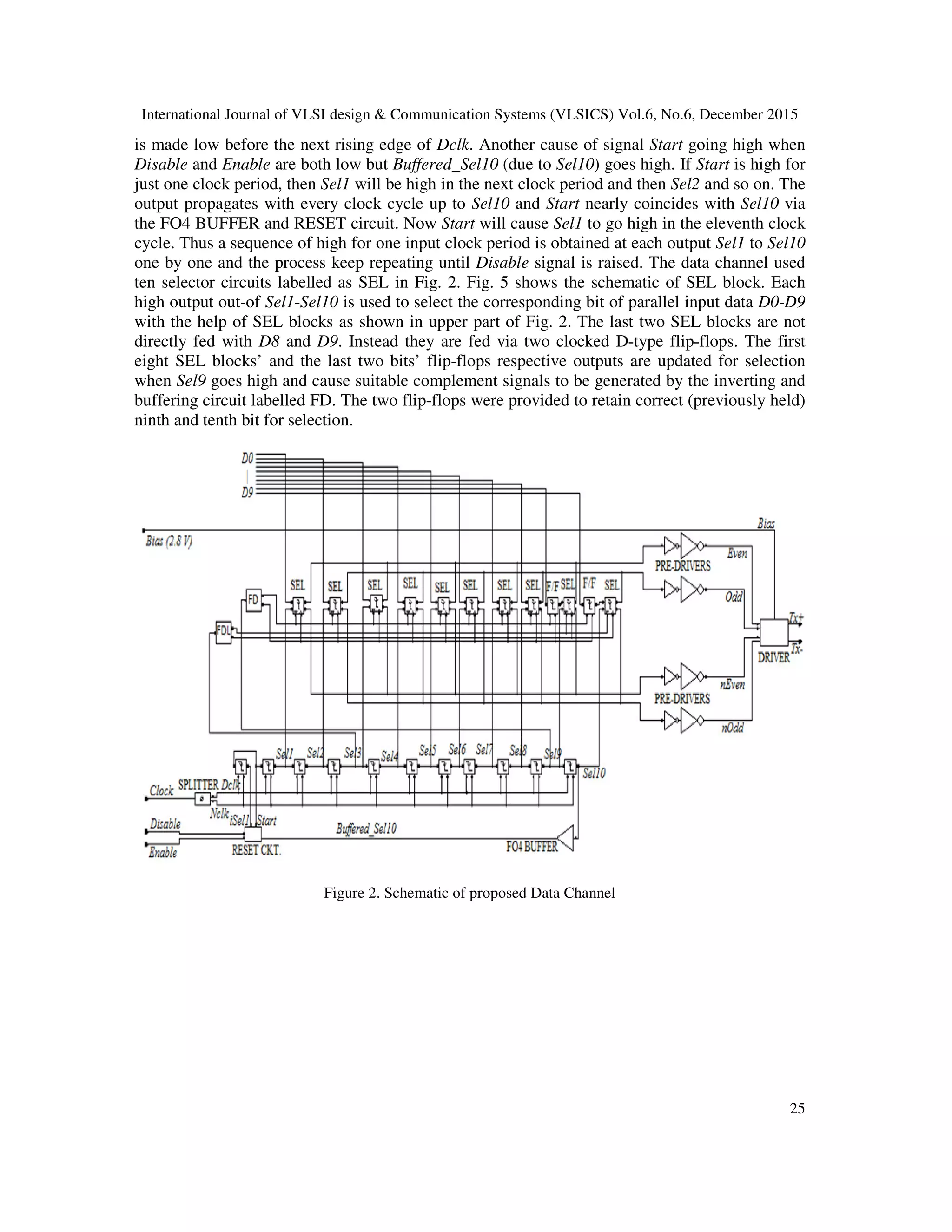
triggered with two nearly complement clock signals Dclk and Nclk obtained from the input Clock
signal by the SPLITTER circuit shown in Fig. 3.
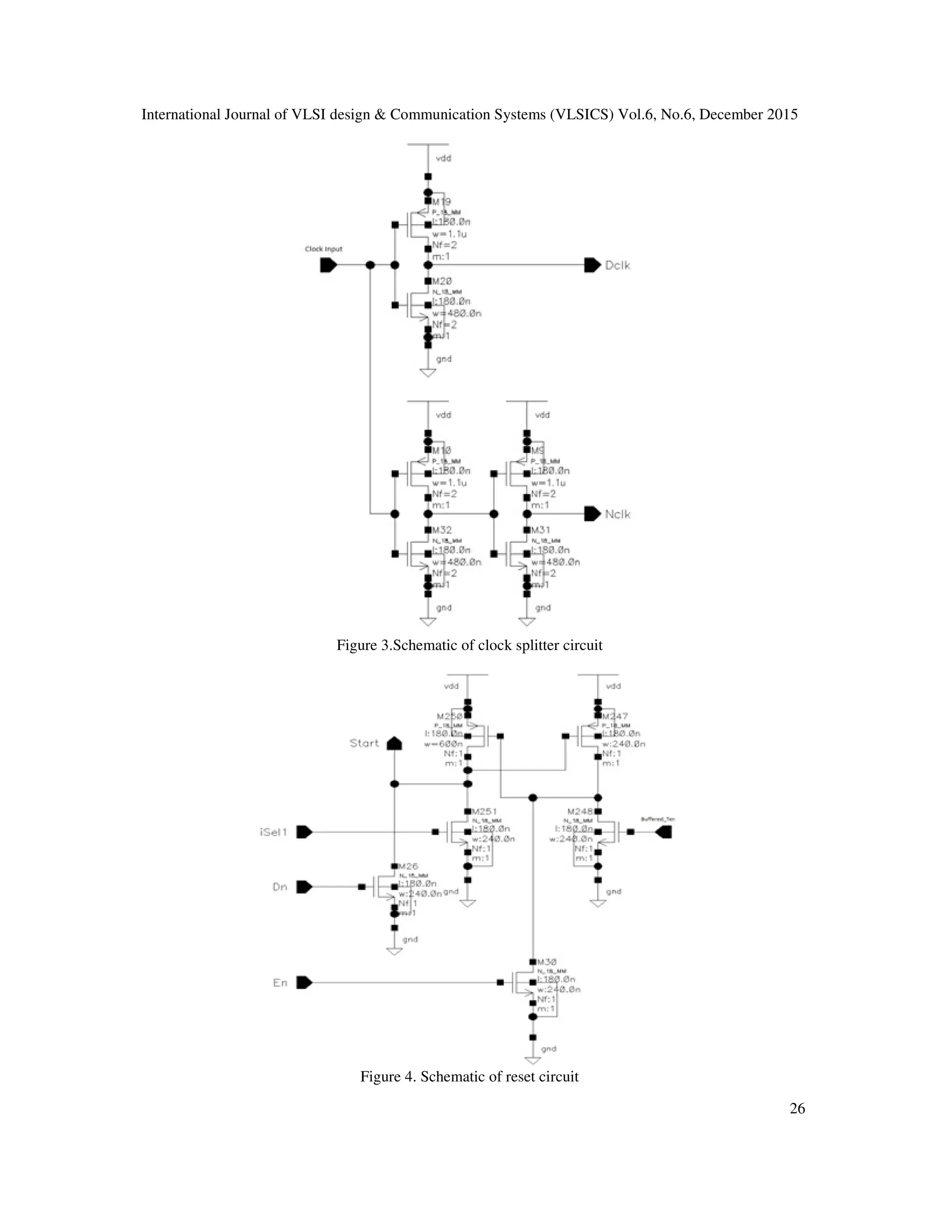
A RESET circuit was provided for disabling and enabling the data channel. The schematic of this
RESET circuit is shown in Fig. 4. The signal Start is driven as high at falling edge of Dclk only if
Disable input was low and Enable input was high at the previous rising edge of Dclk. The Enable](https://image.slidesharecdn.com/6615vlsi03-160107090846/75/Design-of-a-Low-Power-1-65-GBPS-Data-Channel-for-HDMI-Transmitter-2-2048.jpg)
![International Journal of VLSI design & Communication Systems (VLSICS) Vol.6, No.6, December 2015
These two flip-flops update the output with the falling and rising edge respective of their own
clock (Show) and anti-clock (Read) inputs. These inputs are derived from
inverting and buffering circuit labelled as FDL. Hence parallel
first bit selected and kept in hold until all bits are serialized. Thus all correct data bits are selected
in one round of selection from Sel1
data channel.
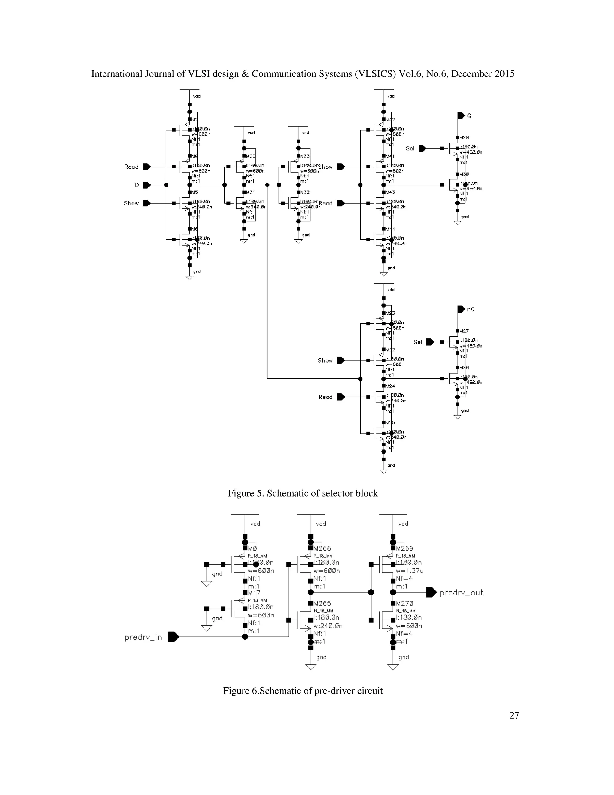
The SELs’ complementary outputs are connected in two groups of even and odd bit periods for
the purpose of pseudo-shadow switching
has its own internal pull-up at the input as shown in
from the five connected SEL outputs. The even and odd pre
parallel pmos transistors in DRIVER circ
multiplexing was achieved. A
differential driving. Fig. 8 shows the proposed layout for the presented design.
Figure 8. Proposed layout of Data Channel
International Journal of VLSI design & Communication Systems (VLSICS) Vol.6, No.6, December 2015
flops update the output with the falling and rising edge respective of their own
clock (Read) inputs. These inputs are derived from Sel3 high level by the
inverting and buffering circuit labelled as FDL. Hence parallel 10 bit data is taken in hold before
first bit selected and kept in hold until all bits are serialized. Thus all correct data bits are selected
Sel1 to Sel10. This is the First-In First-Out (FIFO) action of the
he SELs’ complementary outputs are connected in two groups of even and odd bit periods for
shadow switching [9]. Thus four pre-drivers were used and each pre
up at the input as shown in Fig. 6 so that active low can be multiplexed
from the five connected SEL outputs. The even and odd pre-driver outputs were used to drive the
parallel pmos transistors in DRIVER circuit as shown in Fig.7. Thus 10:1 time
A complementarily active-low driving pair was required for
differential driving. Fig. 8 shows the proposed layout for the presented design.
Figure 7. Schematic of driver circuit
Figure 8. Proposed layout of Data Channel
International Journal of VLSI design & Communication Systems (VLSICS) Vol.6, No.6, December 2015
28
flops update the output with the falling and rising edge respective of their own
high level by the
10 bit data is taken in hold before
first bit selected and kept in hold until all bits are serialized. Thus all correct data bits are selected
Out (FIFO) action of the
he SELs’ complementary outputs are connected in two groups of even and odd bit periods for
drivers were used and each pre-driver
active low can be multiplexed
driver outputs were used to drive the
7. Thus 10:1 time-division
low driving pair was required for](https://image.slidesharecdn.com/6615vlsi03-160107090846/75/Design-of-a-Low-Power-1-65-GBPS-Data-Channel-for-HDMI-Transmitter-6-2048.jpg)
![International Journal of VLSI design & Communication Systems (VLSICS) Vol.6, No.6, December 2015
4. SIMULATION RESULTS
The presented design was simulated using Cadence Virtuoso.
bit-select signals Sel1-Sel10, iSel1
for schematic and post-layout simulation are compared in Table 1.
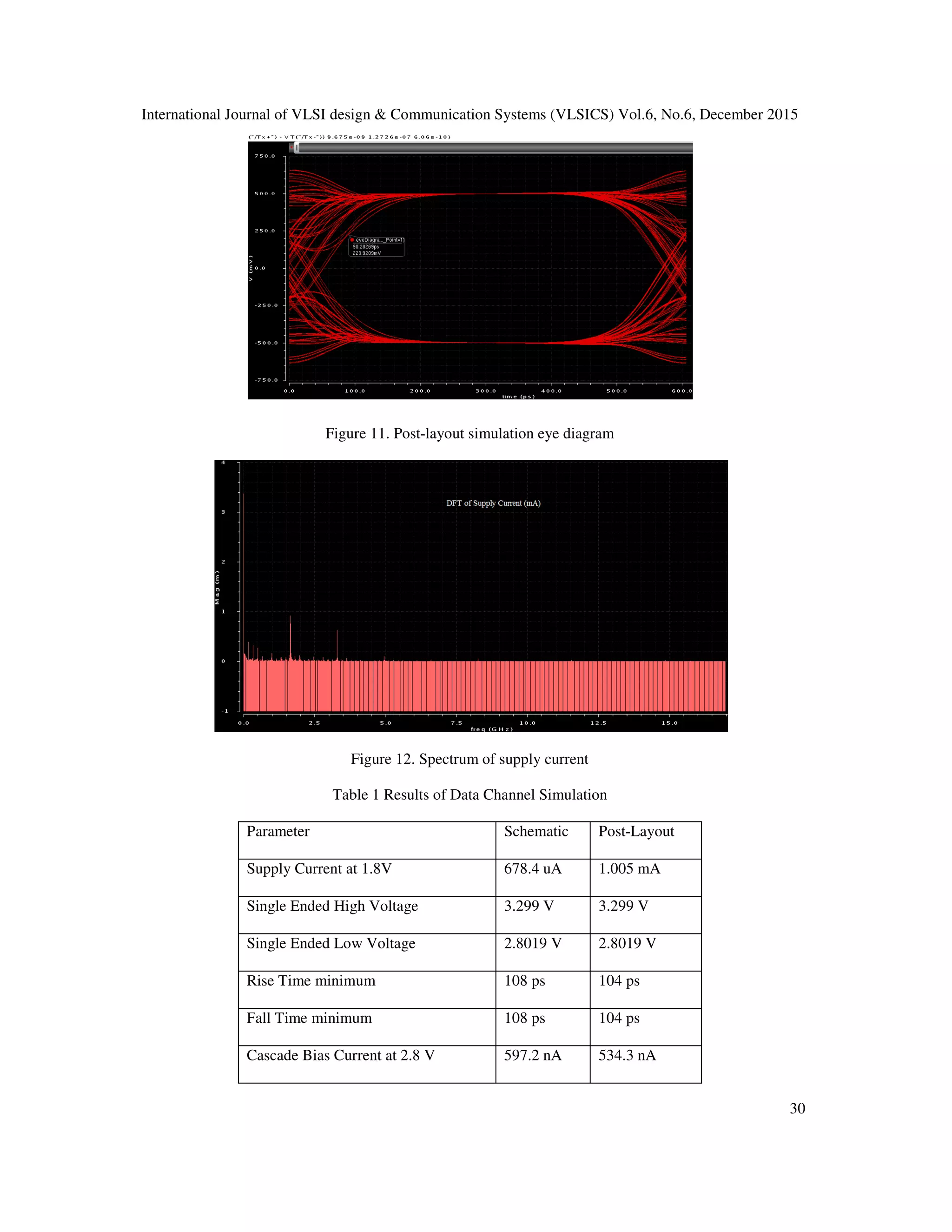
diagram requirements of the HDMI specification and post
10 and 11 respectively. Fig. 12 shows the spectrum of supply current drawn by three as such
presented data channels and one clock channe
within 500 MHz are less than 6% of dc component. The simulation results are compared against
HDMI specification [1] for output voltage requirements in Table 2.
Figure 9. Bit
Figure 10. Eye diagram specification
International Journal of VLSI design & Communication Systems (VLSICS) Vol.6, No.6, December 2015
ESULTS
ed design was simulated using Cadence Virtuoso. During post-layout simulation the
iSel1 and Start signals were obtained as shown in Fig. 9. The
layout simulation are compared in Table 1. The differential output eye
diagram requirements of the HDMI specification and post-layout simulation are displayed in Fig.
10 and 11 respectively. Fig. 12 shows the spectrum of supply current drawn by three as such
presented data channels and one clock channel. As shown in Fig. 12, supply current components
within 500 MHz are less than 6% of dc component. The simulation results are compared against
HDMI specification [1] for output voltage requirements in Table 2.
Figure 9. Bit-select and other signals
Figure 10. Eye diagram specification
International Journal of VLSI design & Communication Systems (VLSICS) Vol.6, No.6, December 2015
29
layout simulation the
signals were obtained as shown in Fig. 9. The results
differential output eye
layout simulation are displayed in Fig.
10 and 11 respectively. Fig. 12 shows the spectrum of supply current drawn by three as such
supply current components
within 500 MHz are less than 6% of dc component. The simulation results are compared against](https://image.slidesharecdn.com/6615vlsi03-160107090846/75/Design-of-a-Low-Power-1-65-GBPS-Data-Channel-for-HDMI-Transmitter-7-2048.jpg)
![International Journal of VLSI design & Communication Systems (VLSICS) Vol.6, No.6, December 2015
31
Table 2. Performance Chart
Item Desired Value [1]
Achieved
Value
Single-ended standby output voltage, Voff 3.290 V < Voff < 3.310 V 3.299 V
Single-ended output swing voltage, Vswing 400mV < Vswing < 600mV 660 mV
Single-ended high level output voltage, VH 3.3 V + 10mV 3.299 V
Single-ended low level output voltage, VL 2.7 V < VL < 2.9 V 2.8019 V
Rise time & fall time (20%-80%)
75 psec < Rise time & 75 psec
< fall time
104 psec &
104 psec
5. CONCLUSIONS
In this paper, a design was presented for data channel of 1.65 Gbps serial speed for application in
HDMI transmitter with low power consumption. The single ended output voltage swing could be
manipulated by controlling the time of over-lap and under-lap of driver’s parallel MOS
transistors by providing additional combinational logic in the serializer. The presented schematic
can also be utilized for other similar high speed serial interfaces like USB and LAN with
applicable modifications.
ACKNOWLEDGEMENTS
The authors would like to thank the Department of Electronics and Instrumentation Engineering,
S.G.S.I.T.S., Indore, India for providing the laboratory facility for performing this work.
REFERENCES
[1] HDMI Licensing, LLC, High-Definition Multimedia Interface Specification Version 1.3a,
http://www.hdmi.org
[2] N. Gupta, T. Nandy, P. S. Sahni, M. Garg, J. N. Tripathi, (2014) “Zero Power 4.95Gbps HDMI
Transmitter”, IEEE International Symposium on Circuits and Systems (ISCAS), Melbourne VIC,
page no. 1500 – 1503.
[3] N. Gupta, P. Bala, V.K. Singh, (2013) “Area and Power Efficient 3.4Gbps/Channel HDMI
Transmitter with Single-Ended Structure”, Proceedings of the 26th International Conference on VLSI
Design and 12th International Conference on Embedded Systems (VLSID), Pune, ISSN: 1063-9667,
page no. 142 – 146.
[4] N. Gupta, T. Nandy, S. Kundu, (2012) “HDMI transmitter in 32nM technology using 28Å MOS”,
IEEE International Symposium on Circuits and Systems (ISCAS), Seoul, ISSN: 0271-4302, page no.
1951 – 1954.](https://image.slidesharecdn.com/6615vlsi03-160107090846/75/Design-of-a-Low-Power-1-65-GBPS-Data-Channel-for-HDMI-Transmitter-9-2048.jpg)
![International Journal of VLSI design & Communication Systems (VLSICS) Vol.6, No.6, December 2015
32
[5] Y. Jeong, et al., (2012) “0.37mW/Gb/s low power SLVS transmitter for battery powered
applications”, IEEE International Symposium on Circuits and Systems (ISCAS), Seoul, ISSN: 0271-
4302, page no. 1955 – 1958.
[6] R. Inti, et al., (2011) “A highly digital 0.5 -to-4Gb/s 1.9mW/Gb/s serial-link transceiver using
current-recycling in 90nm CMOS”, IEEE International Solid-State Circuits Conference Digest of
Technical Papers (ISSCC), San Francisco, CA, ISSN: 0193-6530, page no.152 – 154.
[7] K. Kim, K. Jung, C. Park, W. Park, S. Lee and S. Cho, (2010) “A 3.4Gbps Transmitter for Multi-
Serial Data Communication using pre-emphasis method”, Proceedings of the 4th WSEAS
international conference on Circuits, systems, signal and telecommunications, pp. 153-156.
[8] Y. Suzuki , K. Odagawa and T. Abe, (1973) “Clocked CMOS calculator circuitry”, IEEE J. Solid-
State Circuits, vol. 8, pp.462 -469.
[9] N. Gupta, T. Nandy, P. Bala, (2012) "Self- -Induced Supply Noise Reduction Technique in GBPS
Rate Transmitters", Proceedings of the 25th International Conference on VLSI Design (VLSID), pp.
92, 95, 7-11.](https://image.slidesharecdn.com/6615vlsi03-160107090846/75/Design-of-a-Low-Power-1-65-GBPS-Data-Channel-for-HDMI-Transmitter-10-2048.jpg)

The document discusses the design of a low-power data channel for an HDMI transmitter, operating at a speed of 1.65 Gbps using 180 nm CMOS technology. It employs a single clock input for synchronization and integrates a reset function to manage the data flow efficiently while minimizing power consumption. The design is adaptable for other serial interfaces like USB and LAN with appropriate modifications.