Download to read offline
![IJRET: International Journal of Research in Engineering and Technology eISSN: 2319-1163 | pISSN: 2321-7308
_______________________________________________________________________________________
Volume: 04 Issue: 02 | Feb-2015, Available @ http://www.ijret.org 169
A DESIGN OF MULTIFUNCTIONAL LED WRITTEN SCREEN BASED
ON WIRELESS TRANSMISSION
Yunsheng Gao1
, Shouxi Zhu2
1
Flying College, Binzhou University, Binzhou, Shandong, China
2
Information Technology R&D Center, Binzhou University, Binzhou, Shandong, China
Abstract
This paper presents a design of a LED dot matrix written display system using Single Chip Micyoco (SCM). It completes the data
acquisition function through the light pen with excellent photographic performance phototransistor, then it can achieve the
following functions, such as click light, draw light, reverse display, entire screen erasure, stroke erasure, multi characters written
and so on. The display includes two parts, handwriting screen and color dot matrix screen display, which are connected by
wireless. By light pen writing in the writing area, it can display in color dot matrix display area, it also has the function of key
operation and has a USB interface. Therefore, it can transfer text and picture messages to dot matrix display area. This paper
presents the hardware design and its schematics, gives the general flowchart of software. This design is a low-cost wireless
display design scheme, it has the advantages of simple design, easy to use, etc.
Keywords: LED, Wireless transmission, Light pen, SCM
--------------------------------------------------------------------***----------------------------------------------------------------------
1. INTRODUCTION
LED (Light Emitting Diode) display is a new information
display media developed rapidly in the late eighties on a
global scale. As a new luminous body, LED has been
closely watched from the day it was invented. Especially in
the 21st century, the display technology has entered the era
of flat panel display, LED display as one of the leading flat
panel display products will undoubtedly have greater
development, and it may be one of the representative
mainstream products of flat panel display in the 21st century
[1]. LED dot matrix display screen is currently widely used
in daily life, such as traditional light boxes in outdoor
advertising media, neon lamp and so on which are replaced
by the LED display [2]. However, the traditional control
method of the LED display is by a computer that connected
with LED display, which generally uses the data
transmission standard of RS232 and usually no more than a
maximum baud rate of 115200bps. Its inherent limitations of
low-speed characteristics limit the fast content
synchronization update of LED display, or download the
updated information to the mobile hard disk and then copy it
to the LED display. This control method not only labor
intensive but also cost intensive and inefficient, and bring a
great inconvenience to our work and life.
In recent years, a LED display screen of wireless
transmission has been achieved by sending SMS to the LED
display to achieve information transmission and control [3].
Another common method of wireless transmission is using
GPRS under a mobile communication network for remote
LED display screen on and off and text editing. Those
control methods will not be limited by the distance, but there
may be a series of problems in practical applications, such
as communication delay, information loss, etc.
In this paper, we design a low-cost wireless LED writing
display screen system, which includes two parts of
handwriting dot matrix display screen and color dot matrix
display screen. Both of them are connected by wireless. It
can achieve a variety of functions, such as stroke erasure,
multi characters written, and so on. The biggest advantage
of this design is not dependent on the computer to download
the display information, but by writing on the handwriting
input screen, which greatly solves the problem of high
dependency on the computer.
2. DESIGN OF HARDWARE SYSTEM
The hardware schematic diagram of this design is shown in
figure 1. The system consists of seven parts: main control
module, light pen detection module, LED dot matrix
handwriting input and display module, wireless transmission
module, keyboard input module, LCD real-time status
display, USB flash disk reader module and other
components.](https://image.slidesharecdn.com/adesignofmultifunctionalledwrittenscreenbasedonwirelesstransmission-160829114929/75/A-design-of-multifunctional-led-written-screen-based-on-wireless-transmission-1-2048.jpg)
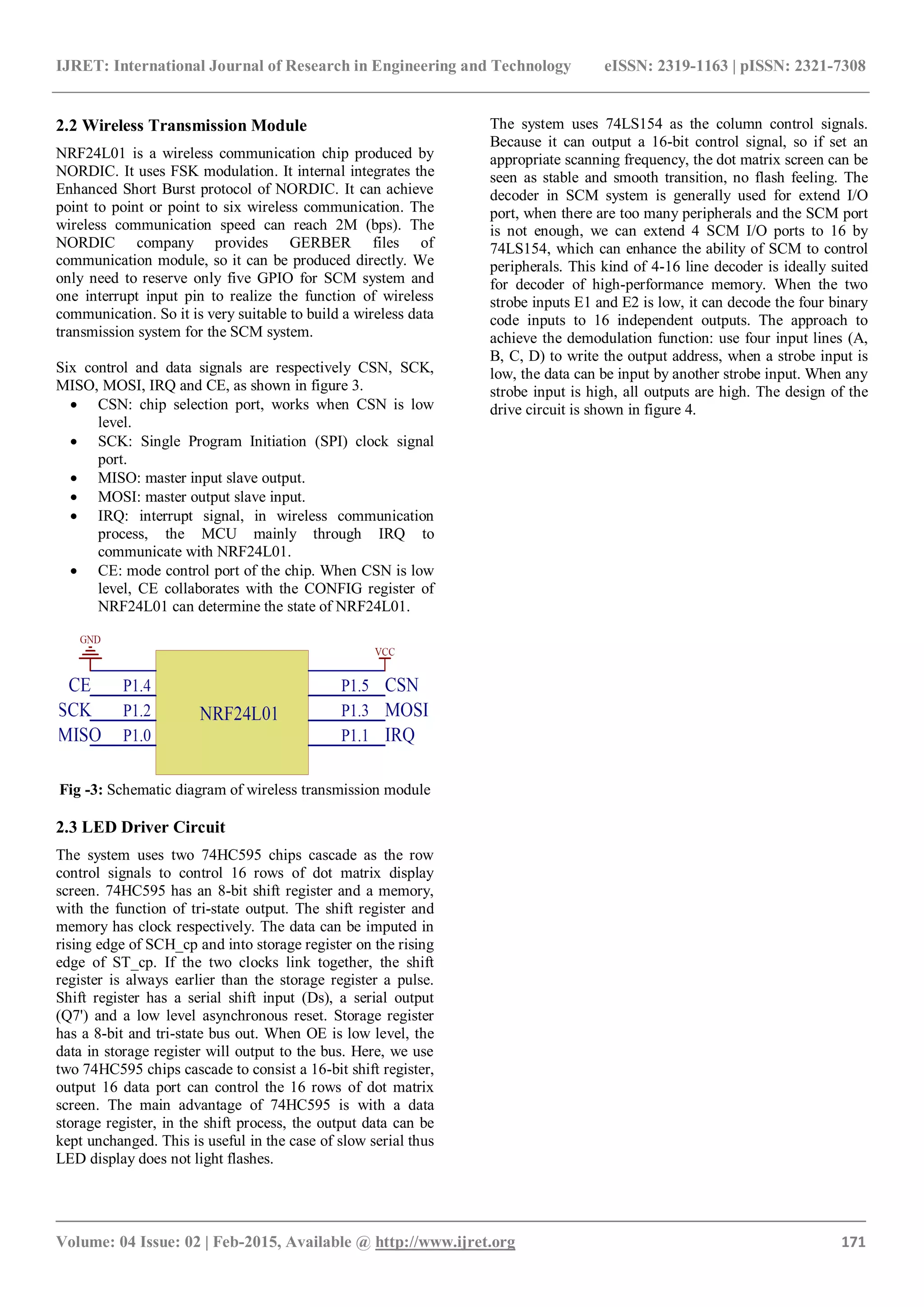
![IJRET: International Journal of Research in Engineering and Technology eISSN: 2319-1163 | pISSN: 2321-7308
_______________________________________________________________________________________
Volume: 04 Issue: 02 | Feb-2015, Available @ http://www.ijret.org 170
Handwriting
input
main control
module
Display
main
control
module
32*32 dot
handwriting
input screen
key module
Light-pen
detection
LCD
module
Wireless
communi
-cation
32*64 dot
display screen
USB flash disk
reader module
Fig -1: Hardware schematic diagram
2.1 Main Control System
As shown in figure 2, in this paper, we use a 89C52 chip as the system master control chip. 89C52 chip is a basic product of
MCS-51 microcontroller series in INTEL Corporation [4]. It is a high-performance 8-bit microcontroller which uses ATMEL
Corporation CMOS process technology, and belongs to the standard MCS-51 product of HCMOS. This chip combines the high-
speed, high-density technology and low-power characteristics of CMOS, which is based on the standard MCS-51 microcontroller
microarchitecture and instruction system. The 89C52 chip is inexpensive but without powerful processing capabilities. In order to
enable it to meet the design requirements, we adopt dynamic scanning [5], the transistor drive in parallel with one side of the LED
light tube, the other foot of LED light tube connect with General Purpose Input/Output (GPIO), and control it on or off. This
method can drive more LED, and is more flexible. It also can save the resources of SCM.
Fig -2: Design of main control system](https://image.slidesharecdn.com/adesignofmultifunctionalledwrittenscreenbasedonwirelesstransmission-160829114929/75/A-design-of-multifunctional-led-written-screen-based-on-wireless-transmission-2-2048.jpg)
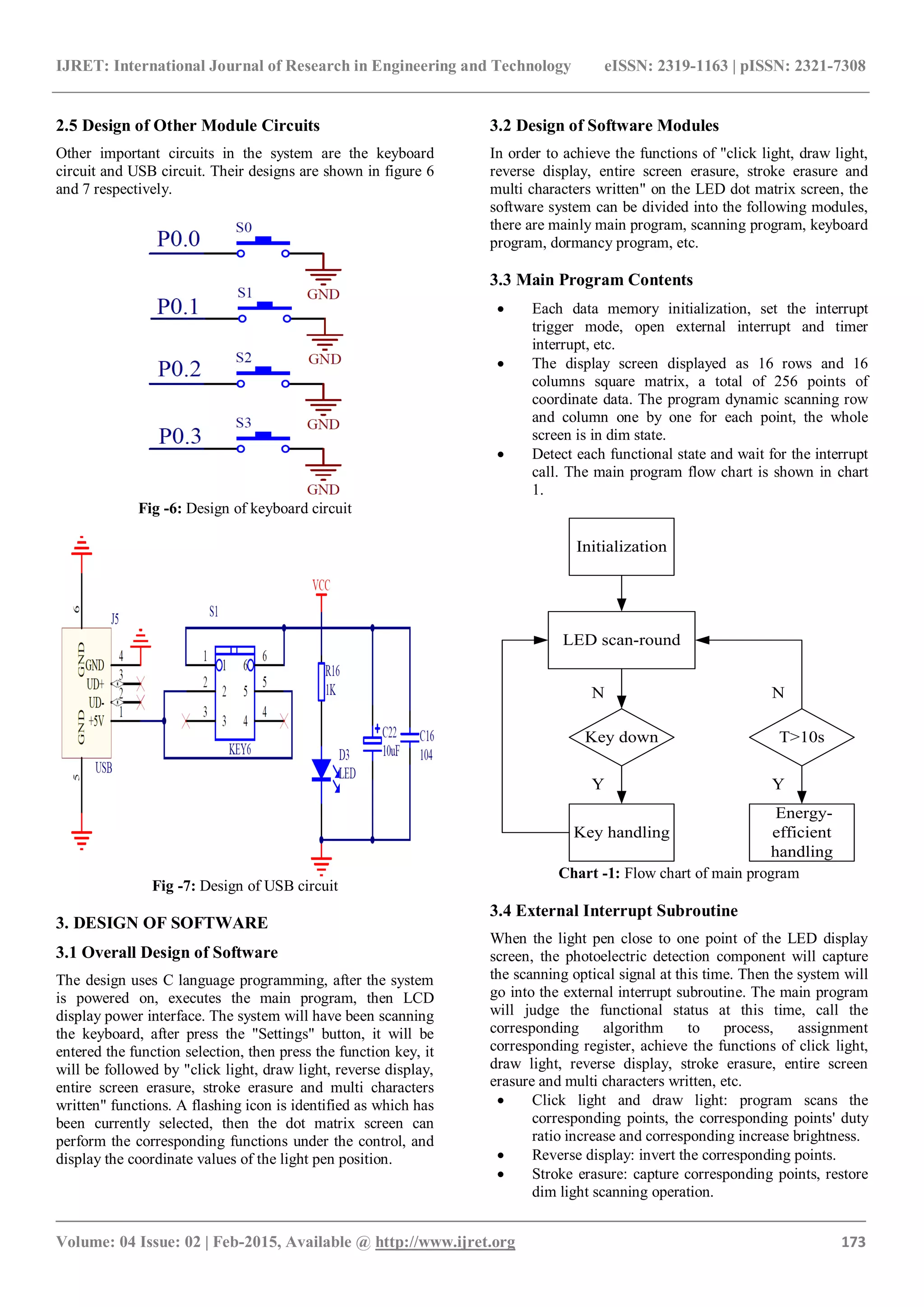
![IJRET: International Journal of Research in Engineering and Technology eISSN: 2319-1163 | pISSN: 2321-7308
_______________________________________________________________________________________
Volume: 04 Issue: 02 | Feb-2015, Available @ http://www.ijret.org 174
Entire screen erasure: the whole screen resumes dim
light scanning operation.
Multi characters written: multiple characters can be
written.
The flow chart of interrupt program is shown in chart 2.
Draw light
Multi characters
written
Erase all
Stroke erasure
Click light
Reverse display
External interruption
Multi characters
written
subroutine
Erase all
subroutine
Stroke erasure
subroutine
Reverse display
subroutine
Draw light
subroutine
Click light
subroutine
RETI
Chart -2: Flow chart of interrupt program
4. CONCLUSION
As a new luminous element, LED has been closely watched
since birth, and LED dot matrix display is widely used in
daily life at present. Currently, the functions of most LED
display screen on the market need computer, so the
operation is complex. This paper proposes a user-friendly
LED dot matrix display. Operators do not need a computer
to control the dot matrix display, only need a matched light
pen to write, and then the character display can be realized.
This design only needs simply manual operation to achieve
information display and don't need the cable transmission,
so it solves the wiring problem. Compared to other LED
display screen, its unique advantage is inexpensive and
greatly reduced the dependence on computer while changing
the operating mode. Core parts of this design are LED
screen and wireless transmission module. These types of
modules are cheap, more economical and practical.
Therefore, in this pursuit of low-carbon green society, this
design has a strong adaptability and broad application
prospects.
ACKNOWLEDGEMENTS
This research was financially supported by National College
Students Innovative Training Program of Binzhou
University (Grant NO. 201310449131).
REFERENCES
[1]. HONG zhen, A Summary of LED Displayer Industry
Development [J]. Information technology &
Standardization, 2010(10): 22-25.
[2]. ZHANG Ming, REN Qing. Some Control and Their
Comparison of LED Scress Display [J]. Journal of Jianghan
University, 2001,18(3): 67-69.
[3]. J. D. Reynders, E. Wright. Practical TCP/IP and
Ethernet Networking [M]. Burlington: IDC Technologies,
2003: 125-127.
[4]. FENG Zhuo-li. The Design of Temperature Control
Heater Based on STC Single-Chip [J]. Techniques of
Automation and Applications, 2014, 33: 104-108.
[5]. Michael Day. TLC5940 dot correction components for
variations in LED brightness [J]. Texas Instruments
Incorporated Power Management, 2005(4): 21-24.
BIOGRAPHIES
Yunsheng Gao is a student in Flying
College of Binzhou University, he is
pursuing Bachelor's Degree in traffic
engineering in Flying College of Binzhou
University, Binzhou, Shandong, China.
Shouxi Zhu (corresponding author) is
working as a teacher and a researcher in
Flying College of Binzhou University. His
research interests include Avionics and
Aviation Human Factor Engineering.
E-mail: zhushouxi@163.com](https://image.slidesharecdn.com/adesignofmultifunctionalledwrittenscreenbasedonwirelesstransmission-160829114929/75/A-design-of-multifunctional-led-written-screen-based-on-wireless-transmission-6-2048.jpg)

This document presents a design for a low-cost multifunctional LED dot matrix written display system using wireless transmission and a light pen for input, minimizing the dependence on computers. The system consists of a handwriting input screen and a color dot matrix display, enabling various functions such as drawing and erasing text without complex setups. The paper details the hardware and software design, including the use of specific microcontrollers and wireless communication chips, highlighting its practical advantages in everyday applications.