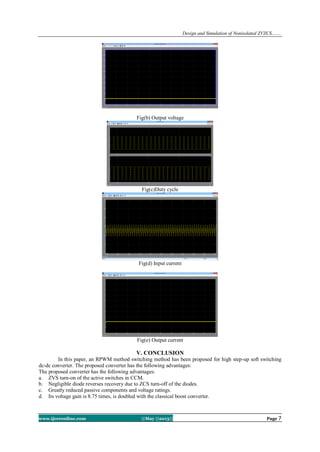
The document summarizes a proposed non-isolated ZVZCS resonant PWM converter for high step-up and high power applications. The proposed converter uses an interleaved structure of basic cells connected in series and parallel to achieve flexibility in device selection. It allows soft-switching turn-on of switches via zero-voltage switching and turn-off of diodes via zero-current switching through the use of an auxiliary circuit. Simulation results are provided to validate the converter's operation and advantages over conventional hard-switched converters, such as reduced switch voltage and current stresses leading to higher efficiency.
![International Journal of Computational Engineering Research||Vol, 03||Issue, 5||
www.ijceronline.com ||May ||2013|| Page 1
Design and Simulation of Nonisolated ZVZCS Resonant PWM Converter
for High Step-Up and High Power Applications
S.M.MohamedSaleem,K.KalaiRaja1
,A.MohamedIlyasMydeen2
,C.R.Mohan Raj
3
,M.Hazina4
1
UG Scholars,**Asst. professor, Syed Ammal Engineering College, Ramanathapuram
Tamil Nadu, India
I. INTRODUCTION
Recently, high step-up dc-dc converters do not require isolation have been used in many applications
such as dc back-up energy systems for Uninterruptible Power Systems(UPS), renewable energy systems, fuel
cell systems and hybrid electric vehicles. Generally, the high step-up dc-dc converter for these applications has
the following requirements.
[1] High step-up voltage gain. Sometimes the voltage gain could be more than 10.
[2] High current handling capability.
[3] High efficiency at a desired level of volume and weight.
[4] Low input current ripple.
In order to provide high output voltage, the classical boost converter should operate at extremely duty
cycle and then the rectifier diode must sustain a short pulse current with high amplitude. This results in severe
reverse recovery as well as high EMI problems. Using an extremely duty cycle may also lead to poor dynamic
responses to line to load variations. Moreover, in the high step up dc-dc converter the input current is usually
large, and hence low voltage rated MOSFETs with small RDS(ON) are necessary in order to reduce the
dominating conduction loss. However, the switch in the classical boost converter should sustain high output
voltage as well, and therefore, the device selection is faced with a contradiction.A lot of step-up dc-dc converter
topologies have been presented to overcome the aforementioned problem. Converters with Coupled inductors
[1]-[5] can provide high output voltage without using high duty cycle and yet reduce the switch voltage stress.
The reverse recovery problem associated with rectifier diode is also alleviated. However, they have large input
current ripple and are not suitable for high power applications since the capacity of the magnetic core is
considerable. The switched-capacitor converter [6]-[10] does not employ an inductor making it feasible to
achieve high power density. However, the efficiency could be reduced to allow output voltage regulation. The
major drawback of these topologies is that attainable voltage gains and power levels without degrading system
performances are restricted.Most of the coupled-inductor and switched-capacitor converters are hard switched
and therefore, they are not suitable for high efficiency and high power applications. Some soft switched
interleaved high step-up converter topologies [11]-[ 18] have been proposed to achieve high efficiency at
desired level of voltage and power level.
In this paper, a new interleaved soft switched high step-up dc-dc converter for high efficiency, high
voltage applications are presented. The proposed converter has the following advantages.
[1] Reduced voltage stresses of switches and diodes,
[2] ZVS turn-on the switches and ZCS turn-off the diodes.
[3] Low input current ripple due to interleaved structure.
[4] Reduced energy volumes of most passive components.
[5] Extendibility to desired voltage gain and power level.
ABSTRACT
This paper proposes a generalized scheme of new soft-switched interleaved boost converters
that is suitable for high step-up and high power applications. The proposed converter is configured with
proper numbers of series and parallel connected basic cells in order to fulfill the required output
voltage and power levels respectively. This leads to flexibility in device selection resulting in high
component availability and easy thermal distribution. Design examples of determining the optimum
circuit configuration for given output voltage gain of 8.75times is presented.
KEY WORDS: High Step-Up, High Voltage Gain, Multiphase, Non-isolated, Soft Switched.](https://image.slidesharecdn.com/a03540109-130614014129-phpapp02/85/A03540109-1-320.jpg)
![International Journal of Computational Engineering Research||Vol, 03||Issue, 5||
www.ijceronline.com ||May ||2013|| Page 1
Design and Simulation of Nonisolated ZVZCS Resonant PWM Converter
for High Step-Up and High Power Applications
S.M.MohamedSaleem,K.KalaiRaja1
,A.MohamedIlyasMydeen2
,C.R.Mohan Raj
3
,M.Hazina4
1
UG Scholars,**Asst. professor, Syed Ammal Engineering College, Ramanathapuram
Tamil Nadu, India
I. INTRODUCTION
Recently, high step-up dc-dc converters do not require isolation have been used in many applications
such as dc back-up energy systems for Uninterruptible Power Systems(UPS), renewable energy systems, fuel
cell systems and hybrid electric vehicles. Generally, the high step-up dc-dc converter for these applications has
the following requirements.
[1] High step-up voltage gain. Sometimes the voltage gain could be more than 10.
[2] High current handling capability.
[3] High efficiency at a desired level of volume and weight.
[4] Low input current ripple.
In order to provide high output voltage, the classical boost converter should operate at extremely duty
cycle and then the rectifier diode must sustain a short pulse current with high amplitude. This results in severe
reverse recovery as well as high EMI problems. Using an extremely duty cycle may also lead to poor dynamic
responses to line to load variations. Moreover, in the high step up dc-dc converter the input current is usually
large, and hence low voltage rated MOSFETs with small RDS(ON) are necessary in order to reduce the
dominating conduction loss. However, the switch in the classical boost converter should sustain high output
voltage as well, and therefore, the device selection is faced with a contradiction.A lot of step-up dc-dc converter
topologies have been presented to overcome the aforementioned problem. Converters with Coupled inductors
[1]-[5] can provide high output voltage without using high duty cycle and yet reduce the switch voltage stress.
The reverse recovery problem associated with rectifier diode is also alleviated. However, they have large input
current ripple and are not suitable for high power applications since the capacity of the magnetic core is
considerable. The switched-capacitor converter [6]-[10] does not employ an inductor making it feasible to
achieve high power density. However, the efficiency could be reduced to allow output voltage regulation. The
major drawback of these topologies is that attainable voltage gains and power levels without degrading system
performances are restricted.Most of the coupled-inductor and switched-capacitor converters are hard switched
and therefore, they are not suitable for high efficiency and high power applications. Some soft switched
interleaved high step-up converter topologies [11]-[ 18] have been proposed to achieve high efficiency at
desired level of voltage and power level.
In this paper, a new interleaved soft switched high step-up dc-dc converter for high efficiency, high
voltage applications are presented. The proposed converter has the following advantages.
[1] Reduced voltage stresses of switches and diodes,
[2] ZVS turn-on the switches and ZCS turn-off the diodes.
[3] Low input current ripple due to interleaved structure.
[4] Reduced energy volumes of most passive components.
[5] Extendibility to desired voltage gain and power level.
ABSTRACT
This paper proposes a generalized scheme of new soft-switched interleaved boost converters
that is suitable for high step-up and high power applications. The proposed converter is configured with
proper numbers of series and parallel connected basic cells in order to fulfill the required output
voltage and power levels respectively. This leads to flexibility in device selection resulting in high
component availability and easy thermal distribution. Design examples of determining the optimum
circuit configuration for given output voltage gain of 8.75times is presented.
KEY WORDS: High Step-Up, High Voltage Gain, Multiphase, Non-isolated, Soft Switched.](https://image.slidesharecdn.com/a03540109-130614014129-phpapp02/75/A03540109-1-2048.jpg)
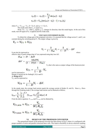
![Design and Simulation of Nonisolated ZVZCS…….
www.ijceronline.com ||May ||2013|| Page 3
Fig. 3. Generalized circuit topology of the proposed interleaved high step-up dc–dc converter (N is the number
of output series-connected basic cell, and P is the number of the output parallel-connected basic cell).
III. CIRCUIT DIAGRAM
Fig. 4.shows the circuit diagram of the proposed converter which has the same circuit topology as the PWM
method proposed in [14]. Fig.5. shows key waveforms illustrating the operating principle of the proposed
converter .The proposed converter consists of a general boost converter as the main circuit and an auxiliary
circuit which includes capacitor Cr, inductor Lr and two diodes DL and
DU.
Fig.4.Circuit diagram of the Proposed Converter
Two switches are operated with asymmetrical complementaryswitching to regulate the output voltage. Owing to
the auxiliary circuit, not only output voltage is raised but ZVS turn-on of two switches can naturally be achieved
in CCM by using energy stored in filter inductor Lf and auxiliary inductor Lr. Unlike PWM method [14] in
which the switches are turned OFF with high peak current the proposed converter utilizes Lr-Crresonance of
auxiliary circuit, thereby reducing the turn-off current of switches. Futhermore, for resonance operation, the
capacitance of Cr is reduced volume. Also, switching losses associated with diode reverse recovery of the
proposed RPWM converter are significantly reduced.
IV. OPERATING PRINCIPLE
The operating modes and key waveforms of the proposed converter are shown in Figs. 5 and 6. In the
below resonance operation, five modes exist within Ts. Mode 1 (t0 – t1 ): This mode begins when upper switch
SU which was carrying the current of difference between iLf and iLris turned OFF. SL can be turned ON with ZVS
if gate signal for SL is applied before the current direction of SL is reversed. Filter inductor current iLf and
auxiliary current iLrstarts to linearly increase and decrease, respectively, as follows
This mode ends when decreasing current iLrchanges its direction of flow. Then DU is turned OFF under ZCS
condition.
Mode 2 (t1-t2) : This mode begins with Lr-Cr resonance of the auxiliary circuit. Current iLf is still linearly
increasing. The voltage and current of resonant components are determined, respectively, as follows:](https://image.slidesharecdn.com/a03540109-130614014129-phpapp02/85/A03540109-3-320.jpg)
![Design and Simulation of Nonisolated ZVZCS…….
www.ijceronline.com ||May ||2013|| Page 8
REFERENCES
[1] K. Hirachi, M. Yamanaka, K. Kajiyama, and S. Isokane, “Circuit configuration of bidirectional DC/DC
converter specific for small scale load leveling system,” in Proc. IEE Power Conv. Conf., Apr. 2002, vol. 2, pp.
603–609.
[2] Q. Zhao and F. C. Lee, “High-efficiency, high step-up DC–DC converters,” IEEE Trans. Power Electron., vol. 18,
no. 1, pp. 65–73, Jan.2003.
[3] T. J. Liang and K. C. Tseng, “Analysis of integrated boost-flyback step-up converter,” in Proc. IEE Electr. Power
Appl., Mar. 2005, vol. 152, no. 2, pp. 217–225.
[4] [4] R. J. Wai and R. Y. Duan, “High-efficiency DC/DC converter with high voltage gain,” in Proc. IEE Electr.
Power Appl., Jul. 2005, vol. 152, no. 4, pp. 793–802.
[5] B. Axelrod, Y. Berkovich, and A. Ioinovici, “Switched coupled-inductor cell for DC–DC converters with very
large conversion ratio,” IEEE Int.Conf. (IECON), pp. 2366–2371, Nov. 2006.
[6] M. S. Makowski, “Realizability conditions and bounds on synthesis of switched-capacitor dc–dc voltage multiplier
circuits,” IEEE Trans. Circuits
[7] Syst. I. Fundam. Theory Appl., vol. 44, no. 8, pp. 684–691, Aug. 1997.
[8] O. C.Mak,Y. C.Wong, andA. Ioinovici, “Step-upDC power supply based on a switched-capacitor circuit,” IEEE
Trans. Ind. Electron., vol. 42, no. 1, pp. 90–97, Feb. 1995.
[9] O. Abutbul, A. Gherlitz, Y. Berkovich, and A. Ioinovici, “Step-up switching-mode converter with high voltage
gain using a switchedcapacitor circuit,” IEEE Trans. Circuits Syst.-I, vol. 50, no. 8, pp. 1098–1102, Aug. 2003.
[10] B. Axelrod, Y. Berkovich, and A. Ioinovici, “Transformerless DC–DC converterswith a very highDCline-to-load
voltage ratio,” in Proc.Circuits Syst., Int. Symp. Circuits Syst. (ISCAS), May 2003, vol. 3, pp. III435– III438.
[11] B. Axelrod, Y. Berkovich, and A. Ioinovici, “Switched-capacitor/switched-inductor structures for getting
transformerless hybrid DC–DC PWM converters,” IEEE Trans. Circuits Syst. I: Regul. Paper, vol. 55, no. 2, pp.
687–696, Mar. 2008.
[12] E. H. Ismail, M. A. Al-Saffar, A. J. Sabzali, and A. A. Fardoun, “A family of single-switch PWM converters with
high step-up conversion ratio,”IEEE Trans. Circuits Syst. I: Regul. Paper, vol. 55, no. 4, pp. 1159–1171, May
2008.
[13] R. Giral, L. S. Martinez, and S. Singer, “Interleaved converters operation basedonCMC,” IEEE Trans. Power
Electron., vol. 14, no. 4, pp. 643–652, Jul. 1999.
[14] P. W. Lee, Y. S. Lee, D. K. Cheng, and X. C. Liu, “Steady-state analysis of an interleaved boost converter with
coupled inductors,” IEEE Trans.Ind. Electron., vol. 47, no. 4, pp. 787–795, Aug. 2000.
[15] B. Huang, I. Sadli, J. P. Martin, and B. Davat, “Design of a high power,high step-up non-isolated DC–DC
converter for fuel cell applications,”IEEE Vehicle Power Propulsion Conf. (VPPC), pp. 1–6, Sep. 2006.
[16] L. Palma, M. H. Todorovic, and P. Enjeti, “A high gain transformer-less DC–DC converter for fuel-cell
applications,” IEEE Power Electron.Spec.Conf. (PESC), pp. 2514–2520, Jun. 2005.
[17] D. Coutellier, V. G. Agelidis, and S. Choi, “Experimental verification of floating-output interleaved-input DC–DC
high-gain transformer-less converter topologies,” IEEE Power Electron. Spec. Conf. (PESC), pp. 562– 568, Jun.
2008.
[18] R. N. A. L. Silva, G. A. L. Henn, P. P. Prac¸a, L. H. S. C. Barreto,D. S. Oliveira, Jr., and F. L. M. Antunes, “Soft-
switching interleaved boost converter with high voltage gain,” IEEE Power Electron. Spec.Conf. (PESC), pp.
4157–4161, Jun. 2008.
[19] W. Li and X. He, “High step-up soft switching interleaved boost converters with cross-winding-coupled inductors
and reduced auxiliary switch number,” IET Power Electron., vol. 2, no. 2, pp. 125–133, Mar. 2009.
[20] S. Park and S. Choi, “Soft-switched CCM boost converters with high voltage gain for high-power applications,”
IEEE Trans. Power Electron.,vol. 25, no. 5, pp. 1211–1217, May 2010.
[21] Dinesh K“ Analysis of Multiphase Boost Converter for High Power Application” International Journal of Applied
Information Systems (IJAIS) – ISSN : 2249-0868 Foundation of Computer Science FCS, New York, USA Volume
1– No.7, March 2012.
[22] R.Saktheeswaran, S.Sulthansikkanderbadusha, A.Parthiban,“ High-Power Applications CCM Boost Converter
with Two Limb Topology Using Soft-Switching Techniques” International Journal of Engineering Research and
Applications (IJERA) ISSN: 2248-9622 Vol. 3, Issue 2, March -April 2013, pp.1752-1756.
[23] Ganga jeyadevi.R, low loss soft-switching boost converter with hi-bridge auxiliary resonant circuit,
International Journal of Communications and Engineering Volume 04– No.4, Issue: 02 March2012.
[24] C.Benin,Dr.M.Sasikumar,“ Simulation And Analysis Of Soft-switching Ccm Boost Converter With High Power
Applications “IOSR Journal of Engineering (IOSRJEN) , Vol. 2 Issue 2, Feb.2012, pp.203-206 .](https://image.slidesharecdn.com/a03540109-130614014129-phpapp02/85/A03540109-8-320.jpg)


![[IJET V2I5P10] Authors: Vinith Das, Dr. Babu Paul, Prof. Elizabeth Seba stian](https://cdn.slidesharecdn.com/ss_thumbnails/ijet-v2i5p10-161107141332-thumbnail.jpg?width=640&height=640&fit=bounds)


![[IJET V2I5P8] Authors: Lakshmi K R, Kavitha Issac, Kiran Boby](https://cdn.slidesharecdn.com/ss_thumbnails/ijet-v2i5p8-161107140749-thumbnail.jpg?width=640&height=640&fit=bounds)


