SlideShare a Scribd company logo
Trim
5
Trim
1
+In
3
–In
2
Output
6
7
+VS
–VS
4
Product
Folder
Sample &
Buy
Technical
Documents
Tools &
Software
Support &
Community
OPA627, OPA637
SBOS165A –SEPTEMBER 2000–REVISED OCTOBER 2015
OPA627 and OPA637 Precision High-Speed Difet®
Operational Amplifiers
The OPA6x7 is fabricated on a high-speed,1 Features
dielectrically-isolated complementary NPN/PNP
1• Very Low Noise: 4.5 nV/√Hz at 10 kHz process. It operates over a wide range of power
• Fast Settling Time: supply voltage of ±4.5 V to ±18 V. Laser-trimmed
Difet input circuitry provides high accuracy and low-– OPA627—550 ns to 0.01%
noise performance comparable with the best bipolar-
– OPA637—450 ns to 0.01%
input operational amplifiers.
• Low VOS: 100-µV maximum
High frequency complementary transistors allow
• Low Drift: 0.8-µV/°C maximum
increased circuit bandwidth, attaining dynamic
• Low IB: 5-pA maximum performance not possible with previous precision FET
operational amplifiers. The OPA627 is unity-gain• OPA627: Unity-Gain Stable
stable. The OPA637 is stable in gains equal to or• OPA637: Stable in Gain ≥ 5
greater than five.
Difet fabrication achieves extremely low input bias2 Applications
currents without compromising input voltage noise
• Precision Instrumentation
performance. Low input bias current is maintained
• Fast Data Acquisition over a wide input common-mode voltage range with
unique cascode circuitry.• DAC Output Amplifier
• Optoelectronics The OPA6x7 is available in plastic PDIP, SOIC, and
metal TO-99 packages. Industrial and military• Sonar, Ultrasound
temperature range models are available.• High-Impedance Sensor Amps
• High-Performance Audio Circuitry Device Information(1)
• Active Filters PART NUMBER PACKAGE BODY SIZE (NOM)
SOIC (8) 3.91 mm × 4.9 mm
3 Description OPA627 PDIP (8) 6.35 mm × 9.81 mm
The OPA6x7 Difet®
operational amplifiers provide a OPA637
8.95 mm (metal can
TO-99 (8)new level of performance in a precision FET diameter)
operational amplifier. When compared to the popular
(1) For all available packages, see the orderable addendum atOPA111 operational amplifier, the OPA6x7 has lower
the end of the data sheet.
noise, lower offset voltage, and higher speed. The
OPA6x7 is useful in a broad range of precision and
high speed analog circuitry.
OPA627 Simplified Schematic
1
An IMPORTANT NOTICE at the end of this data sheet addresses availability, warranty, changes, use in safety-critical applications,
intellectual property matters and other important disclaimers. PRODUCTION DATA.
OPA627, OPA637
SBOS165A –SEPTEMBER 2000–REVISED OCTOBER 2015 www.ti.com
Table of Contents
7.5 Device Functional Modes........................................ 191 Features.................................................................. 1
8 Application and Implementation ........................ 202 Applications ........................................................... 1
8.1 Application Information............................................ 203 Description ............................................................. 1
8.2 Typical Application ................................................. 224 Revision History..................................................... 2
9 Power Supply Recommendations...................... 245 Pin Configuration and Functions......................... 3
10 Layout................................................................... 246 Specifications......................................................... 3
10.1 Layout Guidelines ................................................. 246.1 Absolute Maximum Ratings ...................................... 3
10.2 Layout Example .................................................... 256.2 ESD Ratings ............................................................ 4
11 Device and Documentation Support ................. 266.3 Recommended Operating Conditions....................... 4
11.1 Device Support .................................................... 266.4 Thermal Information.................................................. 4
11.2 Documentation Support ....................................... 266.5 Electrical Characteristics........................................... 5
11.3 Related Links ........................................................ 266.6 Typical Characteristics.............................................. 7
11.4 Trademarks........................................................... 267 Detailed Description ............................................ 12
11.5 Electrostatic Discharge Caution............................ 277.1 Overview ................................................................. 12
11.6 Glossary................................................................ 277.2 Functional Block Diagram ....................................... 12
12 Mechanical, Packaging, and Orderable7.3 Feature Description................................................. 12
Information ........................................................... 277.4 Settling Time ........................................................... 19
4 Revision History
NOTE: Page numbers for previous revisions may differ from page numbers in the current version.
Changes from Original (September 2000) to Revision A Page
• Added ESD Ratings table, Feature Description section, Device Functional Modes, Application and Implementation
section, Power Supply Recommendations section, Layout section, Device and Documentation Support section, and
Mechanical, Packaging, and Orderable Information section. ................................................................................................ 1
• Removed Lead Temperature from Absolute Maximum Ratings table. ................................................................................. 3
2 Submit Documentation Feedback Copyright © 2000–2015, Texas Instruments Incorporated
Product Folder Links: OPA627 OPA637
Offset Trim
–In Output
Offset Trim+In
–VS
+VS
No Internal Connection
Case connected to –VS.
8
1
2
3
4
5
6
7
Offset Trim
–In
+In
–V
No Internal Connection
+V
Output
Offset TrimS
S
1
2
3
4
8
7
6
5
OPA627, OPA637
www.ti.com SBOS165A –SEPTEMBER 2000–REVISED OCTOBER 2015
5 Pin Configuration and Functions
P and D Packages
LMC Package8-Pin PDIP and SOIC
8-Pin TO-99Top View
Top View
Pin Functions
PIN
I/O DESCRIPTION
NO. NAME
1 Offset Trim — Input offset voltage trim (leave floating if not used)
2 –In I Inverting input
3 +In I Noninverting input
4 –VS — Negative (lowest) power supply
5 Offset Trim — Input offset voltage trim (leave floating if not used)
6 Output O Output
7 +VS — Positive (highest) power supply
8 NC — No internal connection (can be left floating)
6 Specifications
6.1 Absolute Maximum Ratings
over operating free-air temperature range (unless otherwise noted) (1)
MIN MAX UNIT
Supply Voltage ±18 V
Input Voltage Range +VS + 2 –VS – 2 V
Differential Input Total VS + 4 V
Power Dissipation 1000 mW
LMC Package –55 125
Operating Temperature °C
P, D Package –40 125
LMC Package 175
Junction Temperature °C
P, D Package 150
LMC Package –65 150
Storage temperature, Tstg °C
P, D Package –40 125
(1) Stresses beyond those listed under Absolute Maximum Ratings may cause permanent damage to the device. These are stress ratings
only, which do not imply functional operation of the device at these or any other conditions beyond those indicated under Recommended
Operating Conditions. Exposure to absolute-maximum-rated conditions for extended periods may affect device reliability.
Copyright © 2000–2015, Texas Instruments Incorporated Submit Documentation Feedback 3
Product Folder Links: OPA627 OPA637
OPA627, OPA637
SBOS165A –SEPTEMBER 2000–REVISED OCTOBER 2015 www.ti.com
6.2 ESD Ratings
VALUE UNIT
OPA627 and OPA637 in PDIP and SOIC Packages
Electrostatic
V(ESD) Human-body model (HBM), per ANSI/ESDA/JEDEC JS-001(1)
±2500 V
discharge
OPA627 and OPA637 in SOIC Packages
Electrostatic
V(ESD) Charged-device model (CDM), per JEDEC specification JESD22-C101(2)
±1000 V
discharge
(1) JEDEC document JEP155 states that 500-V HBM allows safe manufacturing with a standard ESD control process.
(2) JEDEC document JEP157 states that 250-V CDM allows safe manufacturing with a standard ESD control process.
6.3 Recommended Operating Conditions
over operating free-air temperature range (unless otherwise noted)
MIN NOM MAX UNIT
Supply voltage, Vs = (V+) - (V-) 9 (±4.5) 30 (±15) 36 (±18) V
P and D packages –25 25 85 °CSpecified
temperature LMC package –55 25 125 °C
6.4 Thermal Information
OPA627, OPA637
THERMAL METRIC(1)
P (DIP) D (SOIC) LMC (TO-99) UNIT
8 PINS 8 PINS 8 PINS
RθJA Junction-to-ambient thermal resistance 46.2 107.9 200 °C/W
RθJC(top) Junction-to-case (top) thermal resistance 34.5 57.3 — °C/W
RθJB Junction-to-board thermal resistance 23.5 49.7 — °C/W
ψJT Junction-to-top characterization parameter 11.7 11.7 — °C/W
ψJB Junction-to-board characterization parameter 23.3 48.9 — °C/W
RθJC(bot) Junction-to-case (bottom) thermal resistance N/A N/A — °C/W
(1) For more information about traditional and new thermal metrics, see the Semiconductor and IC Package Thermal Metrics application
report, SPRA953.
4 Submit Documentation Feedback Copyright © 2000–2015, Texas Instruments Incorporated
Product Folder Links: OPA627 OPA637
OPA627, OPA637
www.ti.com SBOS165A –SEPTEMBER 2000–REVISED OCTOBER 2015
6.5 Electrical Characteristics
At TA = 25°C, and VS = ±15 V, unless otherwise noted.
PARAMETER TEST CONDITIONS MIN TYP MAX UNIT
OFFSET VOLTAGE(1)
BM, SM grades 40 100
AM grade 130 250
Input offset voltage µV
BP grade 100 250
AP, AU grades 280 500
BM, SM grades 0.4 0.8
AM grade 1.2 2
Average drift µV/°C
BP grade 0.8 2
AP, AU grades 2.5
BM, BP, SM grades 106 120
Power supply rejection VS = ±4.5 to ±18 V dB
AM, AP, AU grades 100 116
INPUT BIAS CURRENT(2)
BM, BP, SM grades 1 5
TA = 25°C pA
AM, AP, AU grades 2 10
VCM = 0 V BM, BP grades 1
Over specified
Input bias current SM grade 50 nA
temperature
AM, AP, AU grades 2
BM, BP, SM grades 1
VCM = ±10 V, over common-mode voltage pA
AM, AP, AU grades 2
BM, BP, SM grades 0.5 5
TA = 25°C pA
AM, AP, AU grades 1 10
Input offset current VCM = 0 V BM, BP grades 1
Over specified
SM grade 50 nA
temperature
AM, AP, AU grades 2
NOISE
BM, BP, SM grades 15 40
f = 10 Hz
AM, AP, AU grades 20
BM, BP, SM grades 8 20
f = 100 Hz
AM, AP, AU grades 10
Input voltage noise density nV/√Hz
BM, BP, SM grades 5.2 8
f = 1 kHz
AM, AP, AU grades 5.6
BM, BP, SM grades 4.5 6
f = 10 kHz
AM, AP, AU grades 4.8
BM, BP, SM grades 0.6 1.6
Input voltage noise BW = 0.1 Hz to 10 Hz µVp-p
AM, AP, AU grades 0.8
BM, BP, SM grades 1.6 2.5Input bias-current noise
f = 100 Hz fA/√Hz
density AM, AP, AU grades 2.5
BM, BP, SM grades 30 60
Input bias-current noise BW = 0.1 Hz to 10 Hz fAp-p
AM, AP, AU grades 48
INPUT IMPEDANCE
Differential Ω || pF1013
|| 8
Common-mode Ω || pF1013
|| 7
INPUT VOLTAGE RANGE
TA = 25°C ±11 ±11.5
Common-mode input range V
Over specified temperature ±10.5 ±11
BM, BP, SM grades 106 116
Common-mode rejection VCM = ±10.5 V dB
AM, AP, AU grades 100 110
(1) Offset voltage measured fully warmed-up.
(2) High-speed test at TJ = 25°C. See Typical Characteristics for warmed-up performance.
Copyright © 2000–2015, Texas Instruments Incorporated Submit Documentation Feedback 5
Product Folder Links: OPA627 OPA637
OPA627, OPA637
SBOS165A –SEPTEMBER 2000–REVISED OCTOBER 2015 www.ti.com
Electrical Characteristics (continued)
At TA = 25°C, and VS = ±15 V, unless otherwise noted.
PARAMETER TEST CONDITIONS MIN TYP MAX UNIT
OPEN-LOOP GAIN
BM, BP, SM grades 112 120
TA = 25°C
AM, AP, AU grades 106 116
Open-loop voltage gain VO = ±10 V, RL = 1kΩ BM, BP grades 106 117 dB
Over specified
SM grade 100 114
temperature
AM, AP, AU grades 100 110
FREQUENCY RESPONSE
G = –1, 10-V step, OPA627 40 55
Slew rate V/µs
G = –4, 10-V step, OPA637 100 135
0.01% 550G = –1, 10-V step,
OPA627 0.1% 450
Settling time ns
0.01% 450G = –4, 10-V step,
OPA637 0.1% 300
G = 1, OPA627 16
Gain-bandwidth product MHz
G = 10, OPA637 80
Total harmonic distortion +
G = 1, f = 1 kHz 0.00003%
noise
POWER SUPPLY
Specified operating voltage ±15 V
Operating voltage range ±4.5 ±18 V
Current ±7 ±7.5 mA
OUTPUT
RL = 1 kΩ ±11.5 ±12.3
Voltage output V
Over specified temperature ±11 ±11.5
Current output VO = ±10 V ±45 mA
Short-circuit current ±35 ±70/–55 ±100 mA
Output impedance, open-loop 1 MHz 55 Ω
TEMPERATURE RANGE
AP, BP, AM, BM, AU grades –25 85Temperature range
°C
specification SM grade –55 125
6 Submit Documentation Feedback Copyright © 2000–2015, Texas Instruments Incorporated
Product Folder Links: OPA627 OPA637
Phase(Degrees)
Gain(dB)
30
20
10
0
–10
–90
–120
–150
–180
–210
1
Phase
Gain
Frequency (MHz)
10 100
75° Phase
Margin
Phase(Degrees)
Gain(dB)
30
20
10
0
–10
–90
–120
–150
–180
–210
1 10 100
Phase
Gain
Frequency (MHz)
Source Resistance ( )
1k
100
10
1
100
OPA627 + Resistor
Resistor Noise Only
Spot Noise
at 10kHz
VoltageNoise(nV/Hz)√
1k 10k 100k 1M 10M 100M
Comparison with
OPA27 Bipolar Op
Amp + Resistor
–
+
RS
Frequency (Hz)
VoltageGain(dB)
1 10 100 1k 10k 100k 1M 10M 100M
140
120
100
80
60
40
20
0
–20
OPA637
OPA627
100
10
1
0.1
0.01
1 10 100 1k 10k 100k 1M 10M
Bandwidth (Hz)
InputVoltageNoise(µV)
Noise Bandwidth:
0.1Hz to indicated
frequency.
RMS
p-p
1k
100
10
1
1
Frequency (Hz)
VoltageNoise(nV/Hz)√
10 100 1k 10k 100k 1M 10M
OPA627, OPA637
www.ti.com SBOS165A –SEPTEMBER 2000–REVISED OCTOBER 2015
6.6 Typical Characteristics
At TA = 25°C, and VS = ±15 V, unless otherwise noted.
Figure 1. Input Voltage Noise Spectral Density vs Frequency Figure 2. Total Input Voltage Noise vs Bandwidth
Figure 3. Voltage Noise vs Source Resistance Figure 4. Open-Loop Gain vs Frequency
Figure 5. OPA627 Gain/Phase vs Frequency Figure 6. OPA637 Gain/Phase vs Frequency
Copyright © 2000–2015, Texas Instruments Incorporated Submit Documentation Feedback 7
Product Folder Links: OPA627 OPA637
Temperature (°C)
CMRandPSR(dB)
125
120
115
110
105
–75
PSR
CMR
–50 –25 0 25 50 75 100 125
Frequency (Hz)
Power-SupplyRejection(dB)
140
120
100
80
60
40
20
0
1
–VS PSRR 627
and 637
+VS PSRR 627
637
10 100 1k 10k 100k 1M 10M
Frequency (Hz)
Common-ModeRejectionRatio(dB)
140
120
100
80
60
40
20
0
1 10 100 1k 10k 100k 1M 10M
OPA627
OPA637
130
120
110
100
90
80
Common-ModeRejection(dB)
Common-Mode Voltage (V)
–15 –10 –5 0 5 10 15
VoltageGain(dB)
Temperature (°C)
125
120
115
110
105
–75 –50 –25 0 25 50 75 100 125
Frequency (Hz)
OutputResistance()
100
80
60
40
20
0
2 20 200 2k 20k 200k 2M 20M
OPA627, OPA637
SBOS165A –SEPTEMBER 2000–REVISED OCTOBER 2015 www.ti.com
Typical Characteristics (continued)
At TA = 25°C, and VS = ±15 V, unless otherwise noted.
Figure 8. Open-Loop Output Impedance vs FrequencyFigure 7. Open-Loop Gain vs Temperature
Figure 9. Common-Mode Rejection vs Frequency Figure 10. Common-Mode Rejection vs Input Common-Mode
Voltage
Figure 11. Power-Supply Rejection vs Frequency Figure 12. Power-Supply Rejection and Common-Mode
Rejection vs Temperature
8 Submit Documentation Feedback Copyright © 2000–2015, Texas Instruments Incorporated
Product Folder Links: OPA627 OPA637
Frequency (Hz)
THD+N(%)
20 100 1k 10k 20k
0.1
0.01
0.001
0.0001
0.00001
G = +10
G = +1
Measurement BW: 80kHz
–
+
–
+
100pF 100pF
G = +1 G = +10
VI VI
549
5k
600600
V = ±10VO V = ±10VO
Frequency (Hz)
THD+N(%)
20 100 1k 10k 20k
1
0.1
0.01
0.001
0.0001
G = +10
G = +50
–
+
100pF
G = +10
VI
549
5k
600
V = ±10VO
–
+
100pF
G = +50
VI
102
5k
600
V = ±10VO
Measurement BW: 80kHz
Temperature (°C)
Gain-Bandwidth(MHz)
24
20
16
12
8
–75
Slew Rate
GBW
60
55
50
SlewRate(V/µs)
–50 –25 0 25 50 75 100 125
Temperature (°C)
Gain-Bandwidth(MHz)
120
100
80
60
40
–75
SlewRate(V/µs)
160
140
120
100
80
Slew Rate
GBW
–50 –25 0 25 50 75 100 125
Temperature (°C)
SupplyCurrent(mA)
8
7.5
7
6.5
6
–75 –50 –25 0 25 50 75 100 125
OutputCurrent(mA)
100
80
60
40
20
0
–75 –50 –25 0 25 50 75 100 125
Temperature (°C)
–IL at VO = –10V
–IL at VO = 0V
+IL at VO = +10V
+IL at VO = 0V
OPA627, OPA637
www.ti.com SBOS165A –SEPTEMBER 2000–REVISED OCTOBER 2015
Typical Characteristics (continued)
At TA = 25°C, and VS = ±15 V, unless otherwise noted.
Figure 13. Supply Current vs Temperature Figure 14. Output Current Limit vs Temperature
Figure 15. OPA627 Gain-Bandwidth and Slew Rate vs Figure 16. OPA637 Gain-Bandwidth and Slew Rate vs
Temperature Temperature
Figure 17. OPA627 Total Harmonic Distortion + Noise vs Figure 18. OPA637 Total Harmonic Distortion + Noise vs
Frequency Frequency
Copyright © 2000–2015, Texas Instruments Incorporated Submit Documentation Feedback 9
Product Folder Links: OPA627 OPA637
Frequency (Hz)
OutputVoltage(Vp-p)
30
20
10
0
100k 1M 10M 100M
OPA627
OPA637
100
10
1
0.1
–1 –10 –100 –1000
Closed-Loop Gain (V/V)
SettlingTime(µs)
Error Band: ±0.01%
OPA637
OPA627
Time From Power Turn-On (Min)
OffsetVoltageChange(µV)
50
25
0
–25
–50
0 1 2 3 4 5 6
Common-Mode Voltage (V)
InputBiasCurrentMultiplier
1.2
1.1
1
0.9
0.8
–15 –10 –5 0 5 10 15
Beyond Linear
Common-Mode Range
Beyond Linear
Common-Mode Range
Junction Temperature (°C)
InputCurrent(pA)
10k
1k
100
10
1
0.1
–50 –25 0 25 50 75 100 125 150
IB
IOS
Supply Voltage (±VS)
InputBiasCurrent(pA)
20
15
10
5
0
±4 ±6 ±8 ±10 ±12 ±14 ±16 ±18
NOTE: Measured fully
warmed-up.
TO-99 with 0807HS Heat Sink
TO-99
Plastic
DIP, SOIC
OPA627, OPA637
SBOS165A –SEPTEMBER 2000–REVISED OCTOBER 2015 www.ti.com
Typical Characteristics (continued)
At TA = 25°C, and VS = ±15 V, unless otherwise noted.
Figure 19. Input Bias and Offset Current vs Junction Figure 20. Input Bias Current vs Power Supply Voltage
Temperature
Figure 21. Input Bias Current vs Common-Mode Voltage Figure 22. Input Offset Voltage Warm-up vs Time
Figure 24. Settling Time vs Closed-Loop GainFigure 23. Maximum Output Voltage vs Frequency
10 Submit Documentation Feedback Copyright © 2000–2015, Texas Instruments Incorporated
Product Folder Links: OPA627 OPA637
1500
1000
500
0
0.001 0.01 0.1 1 10
Error Band (%)
SettlingTime(ns)
OPA637
G = –4
OPA627
G = –1
–
+
CF
RI
RF
2k
+5V
–5V
OPA627 OPA637
RI 2k 500
RF 2k 2k
CF 6pF 4pF
0 150 200 300 400 500
Load Capacitance (pF)
3
2
1
0
SettlingTime(µs)
Error Band:
±0.01%
OPA637
G = –4
OPA627
G = –1
OPA627, OPA637
www.ti.com SBOS165A –SEPTEMBER 2000–REVISED OCTOBER 2015
Typical Characteristics (continued)
At TA = 25°C, and VS = ±15 V, unless otherwise noted.
Figure 25. Settling Time vs Error Band Figure 26. Settling Time vs Load Capacitance
Copyright © 2000–2015, Texas Instruments Incorporated Submit Documentation Feedback 11
Product Folder Links: OPA627 OPA637
Trim
5
Trim
1
+In
3
–In
2
Output
6
7
+VS
–VS
4
OPA627, OPA637
SBOS165A –SEPTEMBER 2000–REVISED OCTOBER 2015 www.ti.com
7 Detailed Description
7.1 Overview
The OPA6x7 Difet operational amplifiers provide a new level of performance in a precision FET operational
amplifier. When compared to the popular OPA111 operational amplifier, the OPA6x7 has lower noise, lower
offset voltage, and higher speed. The OPA6x7 is useful in a broad range of precision and high speed analog
circuitry.
The OPA6x7 is fabricated on a high-speed, dielectrically-isolated complementary NPN/PNP process. It operates
over a wide range of power supply voltage of ±4.5 V to ±18 V. Laser-trimmed Difet input circuitry provides high
accuracy and low-noise performance comparable with the best bipolar-input operational amplifiers.
High frequency complementary transistors allow increased circuit bandwidth, attaining dynamic performance not
possible with previous precision FET operational amplifiers. The OPA627 is unity-gain stable. The OPA637 is
stable in gains equal to or greater than five.
Difet fabrication achieves extremely low input bias currents without compromising input voltage noise
performance. Low input bias current is maintained over a wide input common-mode voltage range with unique
cascode circuitry.
The OPA6x7 is available in plastic PDIP, SOIC, and metal TO-99 packages. Industrial and military temperature
range models are available.
7.2 Functional Block Diagram
7.3 Feature Description
The OPA627 is unity-gain stable. The OPA637 may achieve higher speed and bandwidth in circuits with noise
gain greater than five. Noise gain refers to the closed-loop gain of a circuit, as if the noninverting operational
amplifier input were being driven. For example, the OPA637 may be used in a noninverting amplifier with gain
greater than five, or an inverting amplifier of gain greater than four.
When choosing between the OPA627 or OPA637, consider the high frequency noise gain of your circuit
configuration. Circuits with a feedback capacitor (see Figure 27) place the operational amplifier in unity noise-
gain at high frequency. These applications must use the OPA627 for proper stability. An exception is the circuit in
Figure 28, where a small feedback capacitance is used to compensate for the input capacitance at the inverting
input of the operational amplifier. In this case, the closed-loop noise gain remains constant with frequency, so if
the closed-loop gain is equal to five or greater, the OPA637 may be used.
12 Submit Documentation Feedback Copyright © 2000–2015, Texas Instruments Incorporated
Product Folder Links: OPA627 OPA637
–
+
C2
C1
R2
R1
OPA637
C1 = CIN + CSTRAY
C2 =
R1 C1
R2
–
+
–
+
–
+
–
+
–
+
–
+
Buffer
Bandwidth
Limiting
Integrator Filter
RI
RF < 4R
Inverting Amp
G < |–4|
RI
RF < 4RI
Non-Inverting Amp
G < 5
OPA627 OPA627
OPA627OPA627
OPA627 OPA627
OPA627, OPA637
www.ti.com SBOS165A –SEPTEMBER 2000–REVISED OCTOBER 2015
Feature Description (continued)
Figure 27. Circuits With Noise Gain Less Than Five Require the OPA627 for Proper Stability
Figure 28. Circuits With Noise Gain Equal to or Greater Than Five May Use the OPA637
7.3.1 Offset Voltage Adjustment
The OPA6x7 is laser-trimmed for low offset voltage and drift, so many circuits will not require external
adjustment. Figure 29 shows the optional connection of an external potentiometer to adjust offset voltage. This
adjustment should not be used to compensate for offsets created elsewhere in a system (such as in later
amplification stages or in an A/D converter), because this could introduce excessive temperature drift. Generally,
the offset drift will change by approximately 4 µV/°C for 1 mV of change in the offset voltage due to an offset
adjustment (as shown in Figure 29).
Copyright © 2000–2015, Texas Instruments Incorporated Submit Documentation Feedback 13
Product Folder Links: OPA627 OPA637
–
+
2
3
7
1
5
6
+VS
–VS
OPA627/637
100k
10k to 1M
Potentiometer
(100k preferred)
±10mV Typical
Trim Range
4
OPA627, OPA637
SBOS165A –SEPTEMBER 2000–REVISED OCTOBER 2015 www.ti.com
Feature Description (continued)
Figure 29. Optional Offset Voltage Trim Circuit
7.3.2 Noise Performance
Some bipolar operational amplifiers may provide lower voltage noise performance, but both voltage noise and
bias current noise contribute to the total noise of a system. The OPA6x7 provides both low voltage noise and low
current noise. This provides optimum noise performance over a wide range of sources, including reactive-source
impedances. This can be seen in the performance curve showing the noise of a source resistor combined with
the noise of an OPA627. Above a 2-kΩ source resistance, the operational amplifier contributes little additional
noise. Below 1 kΩ, operational amplifier noise dominates over the resistor noise, but compares favorably with
precision bipolar operational amplifiers.
7.3.3 Input Bias Current
Difet fabrication of the OPA6x7 provides low input bias current. Because the gate current of a FET doubles
approximately every 10°C, to achieve lowest input bias current, keep the die temperature as low as possible. The
high speed, and therefore higher quiescent current, of the OPA6x7 can lead to higher chip temperature. A simple
press-on heat sink such as the Burr-Brown model 807HS (TO-99 metal package) can reduce chip temperature
by approximately 15°C, lowering the IB to one-third its warmed-up value. The 807HS heat sink can also reduce
low-frequency voltage noise caused by air currents and thermoelectric effects. See the data sheet on the 807HS
for details.
Temperature rise in the plastic PDIP and SOIC packages can be minimized by soldering the device to the circuit
board. Wide copper traces also help dissipate heat.
The OPA6x7 may also be operated at reduced power supply voltage, to minimize power dissipation and
temperature rise. Using ±5-V power supplies reduces power dissipation to one-third of that at ±15 V. This
reduces the IB of TO- 99 metal package devices to approximately one-fourth the value at ±15 V.
Leakage currents between printed-circuit-board traces can easily exceed the input bias current of the OPA6x7. A
circuit board guard pattern (see Figure 30) reduces leakage effects. By surrounding critical high impedance input
circuitry with a low impedance circuit connection at the same potential, leakage current will flow harmlessly to the
low-impedance node. The case (TO-99 metal package only) is internally connected to –VS.
Input bias current may also be degraded by improper handling or cleaning. Contamination from handling parts
and circuit boards may be removed with cleaning solvents and deionized water. Each rinsing operation should be
followed by a 30-minute bake at 85°C.
Many FET-input operational amplifiers exhibit large changes in input bias current with changes in input voltage.
Input stage cascode circuitry makes the input bias current of the OPA6x7 virtually constant with wide common-
mode voltage changes. This is ideal for accurate, high input-impedance buffer applications.
14 Submit Documentation Feedback Copyright © 2000–2015, Texas Instruments Incorporated
Product Folder Links: OPA627 OPA637
+VS
5k
(2)
HP 5082-2811
1k
5k
–VS
VO
Diode Bridge
BB: PWS740-3
ZD : 10V IN9611
Clamps output
at VO = ±11.5V
RI
VI –
+
RF
ZD1
OPA627
B.
Board Layout for Input Guarding:
Guard top and bottom of board.
Alternate—use Teflon® standoff for sen-
sitive input pins.
Teflon® E.I. du Pont de Nemours & Co.
–
+
2
3In
Non-inverting
6
OPA627
Out
–
+
2
3
In
Inverting
6
OPA627
Out
–
+
2
3In
Buffer
6
OPA627
Out
3
2
4
5
6
7
8 No Internal Connection
1
TO-99 Bottom View
To Guard Drive
OPA627, OPA637
www.ti.com SBOS165A –SEPTEMBER 2000–REVISED OCTOBER 2015
Feature Description (continued)
Figure 30. Connection of Input Guard for Lowest IB
7.3.4 Phase-Reversal Protection
The OPA6x7 has internal phase-reversal protection. Many FET-input operational amplifiers exhibit a phase
reversal when the input is driven beyond its linear common-mode range. This is most often encountered in
noninverting circuits when the input is driven below –12 V, causing the output to reverse into the positive rail. The
input circuitry of the OPA6x7 does not induce phase reversal with excessive common-mode voltage, so the
output limits into the appropriate rail.
7.3.5 Output Overload
When the inputs to the OPA6x7 are overdriven, the output voltage of the OPA6x7 smoothly limits at
approximately 2.5 V from the positive and negative power supplies. If driven to the negative swing limit, recovery
takes approximately 500 ns. When the output is driven into the positive limit, recovery takes approximately 6 µs.
Output recovery of the OPA627 can be improved using the output clamp circuit shown in Figure 31. Placing
diodes at the inverting input prevent degradation of input bias current.
Figure 31. Clamp Circuit for Improved Overload Recovery
Copyright © 2000–2015, Texas Instruments Incorporated Submit Documentation Feedback 15
Product Folder Links: OPA627 OPA637
R1
–
+
RF
1k
OPA627
CF
G = +1
BW 1MHz
200pF
For Approximate Butterworth Response:
CF =
2 RO CL
RF
RF >> RO
G = 1+
RF
R1
≥
Optional Gain
Gain > 1
f–3dB =
1
2p R√ F RO CF CL
CL
5nF
RO
20
OPA627, OPA637
SBOS165A –SEPTEMBER 2000–REVISED OCTOBER 2015 www.ti.com
Feature Description (continued)
7.3.6 Capacitive Loads
As with any high-speed operational amplifier, best dynamic performance can be achieved by minimizing the
capacitive load. Because a load capacitance presents a decreasing impedance at higher frequency, a load
capacitance which is easily driven by a slow operational amplifier can cause a high-speed operational amplifier to
perform poorly. See the typical curves showing settling times as a function of capacitive load. The lower
bandwidth of the OPA627 makes it the better choice for driving large capacitive loads. Figure 32 shows a circuit
for driving very large load capacitance. The two-pole response of this circuit can also be used to sharply limit
system bandwidth, often useful in reducing the noise of systems which do not require the full bandwidth of the
OPA627.
Figure 32. Driving Large Capacitive Loads
7.3.7 Input Protection
The inputs of the OPA6x7 are protected for voltages from +VS + 2 V to –VS – 2 V. If the input voltage can exceed
these limits, the amplifier should be protected. The diode clamps shown in (a) in Figure 33 prevent the input
voltage from exceeding one forward diode voltage drop beyond the power supplies, which is well within the safe
limits. If the input source can deliver current in excess of the maximum forward current of the protection diodes,
use a series resistor, RS, to limit the current. Be aware that adding resistance to the input increases noise. The 4-
nV/√Hz theoretical thermal noise of a 1-kΩ resistor will add to the 4.5-nV/√Hz noise of the OPA6x7 (by the
square-root of the sum of the squares), producing a total noise of 6 nV/√Hz. Resistors less than 100 Ω add
negligible noise.
Leakage current in the protection diodes can increase the total input bias current of the circuit. The specified
maximum leakage current for commonly used diodes such as the 1N4148 is approximately 25 nA, more than a
thousand times larger than the input bias current of the OPA6x7. Leakage current of these diodes is typically
much lower and may be adequate in many applications. Light falling on the junction of the protection diodes can
dramatically increase leakage current, so common glass-packaged diodes should be shielded from ambient light.
Very low leakage can be achieved by using a diode-connected FET as shown. The 2N4117A is specified at 1 pA
and its metal case shields the junction from light.
Sometimes input protection is required on I/V converters of inverting amplifiers; see (b) in Figure 33. Although in
normal operation, the voltage at the summing junction will be near zero (equal to the offset voltage of the
amplifier), and large input transients may cause this node to exceed 2 V beyond the power supplies. In this case,
the summing junction should be protected with diode clamps connected to ground. Even with the low voltage
present at the summing junction, common signal diodes may have excessive leakage current. Because the
reverse voltage on these diodes is clamped, a diode-connected signal transistor can act as an inexpensive low
leakage diode; see (b) in Figure 33.
16 Submit Documentation Feedback Copyright © 2000–2015, Texas Instruments Incorporated
Product Folder Links: OPA627 OPA637
–
+
–VS
+VS
Optional RS
VO
D: IN4148 — 25nA Leakage
2N4117A — 1pA Leakage
(a)
=
–
+
IIN
VO
D
D
D
(b)
D
D: 2N3904
=
NC
Siliconix
OPA627
OPA627
OPA627, OPA637
www.ti.com SBOS165A –SEPTEMBER 2000–REVISED OCTOBER 2015
Feature Description (continued)
Figure 33. Input Protection Circuits
7.3.8 EMI Rejection Ratio (EMIRR)
The electromagnetic interference (EMI) rejection ratio, or EMIRR, describes the EMI immunity of operational
amplifiers. An adverse effect that is common to many operational amplifiers is a change in the offset voltage as a
result of RF signal rectification. An operational amplifier that is more efficient at rejecting this change in offset as
a result of EMI has a higher EMIRR and is quantified by a decibel value. Measuring EMIRR can be performed in
many ways, but this report provides the EMIRR IN+, which specifically describes the EMIRR performance when
the RF signal is applied to the noninverting input pin of the operational amplifier. In general, only the noninverting
input is tested for EMIRR for the following three reasons:
• Operational amplifier input pins are known to be the most sensitive to EMI, and typically rectify RF signals
better than the supply or output pins.
• The noninverting and inverting operational amplifier inputs have symmetrical physical layouts and exhibit
nearly matching EMIRR performance.
• EMIRR is easier to measure on noninverting pins than on other pins because the noninverting input terminal
can be isolated on a printed-circuit-board (PCB). This isolation allows the RF signal to be applied directly to
the noninverting input terminal with no complex interactions from other components or connecting PCB
traces.
A more formal discussion of the EMIRR IN+ definition and test method is provided in application report EMI
Rejection Ratio of Operational Amplifiers (SBOA128), available for download at www.ti.com.
The EMIRR IN+ of the OPA627 is plotted versus frequency as shown in Figure 34. If available, any dual and
quad operational amplifier device versions have nearly similar EMIRR IN+ performance. The OPA627 unity-gain
bandwidth is 16 MHz. EMIRR performance below this frequency denotes interfering signals that fall within the
operational amplifier bandwidth.
Copyright © 2000–2015, Texas Instruments Incorporated Submit Documentation Feedback 17
Product Folder Links: OPA627 OPA637
Frequency (MHz)
EMIRRIN+(db)
0
20
40
60
80
100
120
140
10M 100M 1G 10G
PRF = -10 dbm
VS = r15 V
VCM = 0 V
OPA627, OPA637
SBOS165A –SEPTEMBER 2000–REVISED OCTOBER 2015 www.ti.com
Feature Description (continued)
Figure 34. OPA627 EMIRR IN+ vs Frequency
Table 1 shows the EMIRR IN+ values for the OPA627 at particular frequencies commonly encountered in real-
world applications. Applications listed in Table 1 may be centered on or operated near the particular frequency
shown. This information may be of special interest to designers working with these types of applications, or
working in other fields likely to encounter RF interference from broad sources, such as the industrial, scientific,
and medical (ISM) radio band.
Table 1. OPA627 EMIRR IN+ for Frequencies of Interest
FREQUENCY APPLICATION / ALLOCATION EMIRR IN+
400 MHz Mobile radio, mobile satellite/space operation, weather, radar, UHF 46.2 dB
GSM, radio com/nav./GPS (to 1.6 GHz), ISM, aeronautical mobile,
900 MHz 60.3 dB
UHF
1.8 GHz GSM, mobile personal comm. broadband, satellite, L-band 81 dB
802.11b/g/n, Bluetooth™, mobile personal comm., ISM, amateur
2.4 GHz 96.9 dB
radio/satellite, S-band
3.6 GHz Radiolocation, aero comm./nav., satellite, mobile, S-band 108.9 dB
802.11a/n, aero comm./nav., mobile comm., space/satellite
5 Ghz 116.8 dB
operation, C-band
7.3.8.1 EMIRR IN+ Test Configuration
Figure 35 shows the circuit configuration for testing the EMIRR IN+. An RF source is connected to the
operational amplifier noninverting input terminal using a transmission line. The operational amplifier is configured
in a unity gain buffer topology with the output connected to a low-pass filter (LPF) and a digital multimeter
(DMM). A large impedance mismatch at the operational amplifier input causes a voltage reflection; however, this
effect is characterized and accounted for when determining the EMIRR IN+. The resulting DC offset voltage is
sampled and measured by the multimeter. The LPF isolates the multimeter from residual RF signals that may
interfere with multimeter accuracy. Refer to SBOA128 for more details.
18 Submit Documentation Feedback Copyright © 2000–2015, Texas Instruments Incorporated
Product Folder Links: OPA627 OPA637
OPA627 OPA637
RI, R1 2k 500
CF 6pF 4pF
Error Band ±0.5mV ±0.2mV
(0.01%)
NOTE: CF is selected for best settling time performance
depending on test fixture layout. Once optimum value is
determined, a fixed capacitor may be used.
–
+
±5V
Out
+15V
2k
CF
2kW
Error Out
RI
RI
51
–15V
HP-
5082-
2835
High Quality
Pulse Generator
/
+
±
Low-Pass Filter50
Digital Multimeter
Ambient temperature: 25Û&
Sample /
Averaging
+VS
-VS
Not shown: 0.1 µF and 10 µF
supply decoupling
RF source
DC Bias: 0 V
Modulation: None (CW)
Frequency Sweep: 201 pt. Log
OPA627, OPA637
www.ti.com SBOS165A –SEPTEMBER 2000–REVISED OCTOBER 2015
Figure 35. EMIRR IN+ Test Configuration Schematic
7.4 Settling Time
The OPA627 and OPA637 have fast settling times, as low as 300 ns. Figure 36 illustrates the circuit used to
measure settling time for the OPA627 and OPA637.
Figure 36. Settling Time and Slew Rate Test Circuit
7.5 Device Functional Modes
The OPA627 and OPA6377 have a single functional mode and are operational when the power-supply voltage is
greater than 9V (±4.5 V). The maximum power supply voltage for the OPA627 and OPA637 are 36 V (±18 V).
Copyright © 2000–2015, Texas Instruments Incorporated Submit Documentation Feedback 19
Product Folder Links: OPA627 OPA637
This composite amplifier uses the OPA603 current-feedback op amp to
provide extended bandwidth and slew rate at high closed-loop gain. The
feedback loop is closed around the composite amp, preserving the
precision input characteristics of the OPA627/637. Use separate power
supply bypass capacitors for each op amp.
GAIN A1 R1 R2 R3 R4 –3dB SLEW RATE
(V/V) OP AMP (W ) (k ) ( ) (k ) (MHz) (V/µs)
100 OPA627 50.5(1) 4.99 20 1 15 700
1000 OPA637 49.9 4.99 12 1 11 500
NOTE: (1) Closest 1/2% value.
∗Minimize capacitance at this node.+
–
OPA603
–
+
A1
R3
R1
R4
R2
VI VO
*
RL ‡ 150
for ±10V Out
–In
+In
+
–
OPA637
Differential Voltage Gain = (1 + 2RF/RG) • 10
2
3
–
+
–
+
INA106
Differential
Amplifier
1
6
5
Output
Gain = 1000
CMRR 116dB
Bandwidth 400kHz
OPA637
10k
10k
100k
100k
Input Common-Mode
Range = ±10V
»
»
3pF
RF
5k
RF
5k
RG
101
–In
+In
+
–
OPA637
Differential Voltage Gain = 1 + 2RF/RG
2
3
–
+
–
+
INA105
Differential
Amplifier
1
6
5
Output
Gain = 100
CMRR 116dB
Bandwidth 1MHz
OPA637
25k
25k
25k
25k
Input Common-Mode
Range = ±5V
»
»
3pF
RF
5k
RF
5kW
RG
101
OPA627, OPA637
SBOS165A –SEPTEMBER 2000–REVISED OCTOBER 2015 www.ti.com
8 Application and Implementation
NOTE
Information in the following applications sections is not part of the TI component
specification, and TI does not warrant its accuracy or completeness. TI’s customers are
responsible for determining suitability of components for their purposes. Customers should
validate and test their design implementation to confirm system functionality.
8.1 Application Information
The OPA627 and OPA637 are ideally suited to use as input amplifiers in instrumentation amplifier configurations
requiring high speed, fast settling and high input impedance.
Figure 37. High Speed Instrumentation Amplifier, Gain = 100
Figure 38. High Speed Instrumentation Amplifier, Gain = 1000
Figure 39. Composite Amplifier for Wide Bandwidth
20 Submit Documentation Feedback Copyright © 2000–2015, Texas Instruments Incorporated
Product Folder Links: OPA627 OPA637
When driven with a very fast input step (left), common-mode
transients cause a slight variation in input stage currents which
will reduce output slew rate. If the input step slew rate is reduced
(right), output slew rate will increase slightly.
NOTE: (1) Optimum value will
depend on circuit board lay-
out and stray capacitance at
the inverting input.
LARGE SIGNAL RESPONSE
+10
0
–10
VOUT(V)
+10
0
–10
(C) (D)
VOUT(V)
–
+
OPA627
G = –1
2k
2k
6pF(1)
VOUT
FPO
When used as a unity-gain buffer, large common-mode input voltage steps
produce transient variations in input-stage currents. This causes the rising
edge to be slower and falling edges to be faster than nominal slew rates
observed in higher-gain circuits.
(A) (B)
SMALL SIGNAL RESPONSELARGE SIGNAL RESPONSE
–
+
OPA627
G = 1
OPA627, OPA637
www.ti.com SBOS165A –SEPTEMBER 2000–REVISED OCTOBER 2015
Application Information (continued)
Figure 40. OPA627 Dynamic Performance, G = 1
Figure 41. OPA627 Dynamic Performance, G = –1
Copyright © 2000–2015, Texas Instruments Incorporated Submit Documentation Feedback 21
Product Folder Links: OPA627 OPA637
1 3 2 5
2
2 1 3 4 3 4 2 5
1 R R C COutput
s
Input s s C 1 R 1 R 1 R 1 R R C C
+
±
OPA627
Output
Input
R1
590
R4
2.94 k
R3
499
C2
39 nF
C5
1 nF
OPA637
LARGE SIGNAL RESPONSE
OPA637
SMALL SIGNAL RESPONSE
FPO
–10
0
+10
–100
0
+100
(F)(E)
–
+
OPA637
G = 5
2k
500
4pF(1)
VOUT
NOTE: (1) Optimum value will depend on circuit
board layout and capacitance at inverting input.
VOUT(V)
VOUT(mV)
OPA627, OPA637
SBOS165A –SEPTEMBER 2000–REVISED OCTOBER 2015 www.ti.com
Application Information (continued)
Figure 42. OPA637 Dynamic Response, G = 5
8.2 Typical Application
Low pass filters are commonly employed in signal processing applications to reduce noise and prevent aliasing.
The OPA627 and OPA637 are ideally suited to construct high speed, high precision active filters. Figure 43
illustrates a second order low pass filter commonly encountered in signal processing applications.
Figure 43. Second Order Low Pass Filter
8.2.1 Design Requirements
Use the following parameters for this design example:
• Gain = 5 V/V (inverting gain)
• Low pass cutoff frequency = 25 kHz
• Second order Chebyshev filter response with 3-dB gain peaking in the passband
8.2.2 Detailed Design Procedure
The infinite-gain multiple-feedback circuit for a low-pass network function is shown in Figure 43. Use Equation 1
to calculate the voltage transfer function.
(1)
22 Submit Documentation Feedback Copyright © 2000–2015, Texas Instruments Incorporated
Product Folder Links: OPA627 OPA637
Frequency (Hz)
Gain(db)
-60
-40
-20
0
20
100 1k 10k 100k 1M
4
1
C 3 4 2 5
R
Gain
R
1
f 1 R R C C
2S
OPA627, OPA637
www.ti.com SBOS165A –SEPTEMBER 2000–REVISED OCTOBER 2015
Typical Application (continued)
This circuit produces a signal inversion. For this circuit the gain at DC and the low pass cutoff frequency can be
calculated using Equation 2.
(2)
Software tools are readily available to simplify filter design. WEBENCH® Filter Designer is a simple, powerful,
and easy-to-use active filter design program. The WEBENCH Filter Designer lets you create optimized filter
designs using a selection of TI operational amplifiers and passive components from TI's vendor partners.
Available as a web based tool from the WEBENCH® Design Center, WEBENCH® Filter Designer allows you to
design, optimize, and simulate complete multi-stage active filter solutions within minutes.
8.2.3 Application Curve
Figure 44. OPA627 2nd Order 25 kHz, Chebyshev, Low Pass Filter
Copyright © 2000–2015, Texas Instruments Incorporated Submit Documentation Feedback 23
Product Folder Links: OPA627 OPA637
OPA627, OPA637
SBOS165A –SEPTEMBER 2000–REVISED OCTOBER 2015 www.ti.com
9 Power Supply Recommendations
The OPA627 and OPA637 are specified for operation from 9 V to 36 V (±4.5 V to ±18 V); many specifications
apply from –25°C to 85°C (P and D packages) and –55°C to 125°C (LMC package). Parameters that can exhibit
significant variance with regard to operating voltage or temperature are presented in the Typical Characteristics.
10 Layout
10.1 Layout Guidelines
For best operational performance of the device, use good PCB layout practices, including:
• Noise can propagate into analog circuitry through the power pins of the circuit as a whole and operational
amplifier itself. Bypass capacitors are used to reduce the coupled noise by providing low-impedance
power sources local to the analog circuitry.
– Connect low-ESR, 0.1-µF ceramic bypass capacitors between each supply pin and ground, placed as
close to the device as possible. A single bypass capacitor from V+ to ground is applicable for single-
supply applications.
– The OPA6x7 is capable of high-output current (in excess of 45 mA). Applications with low impedance
loads or capacitive loads with fast transient signals demand large currents from the power supplies.
Larger bypass capacitors such as 1-µF solid tantalum capacitors may improve dynamic performance
in these applications.
• Separate grounding for analog and digital portions of circuitry is one of the simplest and most-effective
methods of noise suppression. One or more layers on multilayer PCBs are usually devoted to ground
planes. A ground plane helps distribute heat and reduces EMI noise pickup. Make sure to physically
separate digital and analog grounds paying attention to the flow of the ground current. For more detailed
information refer to Circuit Board Layout Techniques (SLOA089).
• To reduce parasitic coupling, run the input traces as far away from the supply or output traces as
possible. If these traces cannot be kept separate, crossing the sensitive trace perpendicular is much
better as opposed to in parallel with the noisy trace.
• Place the external components as close to the device as possible. As shown in Figure 45, keeping RF
and RG close to the inverting input minimizes parasitic capacitance.
• Keep the length of input traces as short as possible. Always remember that the input traces are the most
sensitive part of the circuit.
• Consider a driven, low-impedance guard ring around the critical traces. A guard ring can significantly
reduce leakage currents from nearby traces that are at different potentials.
• The case (TO-99 metal package only) is internally connected to the negative power supply, as with most
common operational amplifiers.
• Pin 8 of the plastic PDIP, SOIC, and TO-99 packages has no internal connection.
• Cleaning the PCB following board assembly is recommended for best performance.
• Any precision integrated circuit may experience performance shifts due to moisture ingress into the
plastic package. Following any aqueous PCB cleaning process, baking the PCB assembly is
recommended to remove moisture introduced into the device packaging during the cleaning process. A
low temperature, post cleaning bake at 85°C for 30 minutes is sufficient for most circumstances.
24 Submit Documentation Feedback Copyright © 2000–2015, Texas Instruments Incorporated
Product Folder Links: OPA627 OPA637
B.
Board Layout for Input Guarding:
Guard top and bottom of board.
Alternate—use Teflon® standoff for sen-
sitive input pins.
Teflon® E.I. du Pont de Nemours & Co.
–
+
2
3In
Non-inverting
6
OPA627
Out
–
+
2
3
In
Inverting
6
OPA627
Out
–
+
2
3In
Buffer
6
OPA627
Out
3
2
4
5
6
7
8 No Internal Connection
1
TO-99 Bottom View
To Guard Drive
Offset trim
±IN
+IN
V±
V+
OUTPUT
NC
Offset trim
VS+
GND
VS±
GND
Ground (GND) plane on another layer
VOUT
VIN
GND
Run the input traces
as far away from
the supply lines
as possible
Use low-ESR, ceramic
bypass capacitor
RF
RG
Place components
close to device and to
each other to reduce
parasitic errors
+VIN
VOUTRG
RF
(Schematic Representation)
Use low-ESR,
ceramic bypass
capacitor
OPA627, OPA637
www.ti.com SBOS165A –SEPTEMBER 2000–REVISED OCTOBER 2015
10.2 Layout Example
Figure 45. OPA627 Layout Example for the Noninverting Configuration
Figure 46. Board Layout for Input Guarding (LMC Package)
Copyright © 2000–2015, Texas Instruments Incorporated Submit Documentation Feedback 25
Product Folder Links: OPA627 OPA637
OPA627, OPA637
SBOS165A –SEPTEMBER 2000–REVISED OCTOBER 2015 www.ti.com
11 Device and Documentation Support
11.1 Device Support
11.1.1 Development Support
11.1.1.1 TINA-TI™ (Free Software Download)
TINA™ is a simple, powerful, and easy-to-use circuit simulation program based on a SPICE engine. TINA-TI is a
free, fully-functional version of the TINA software, preloaded with a library of macro models in addition to a range
of both passive and active models. TINA-TI provides all the conventional dc, transient, and frequency domain
analysis of SPICE, as well as additional design capabilities.
Available as a free download from the Analog eLab Design Center, TINA-TI offers extensive post-processing
capability that allows users to format results in a variety of ways. Virtual instruments offer the ability to select
input waveforms and probe circuit nodes, voltages, and waveforms, creating a dynamic quick-start tool.
WEBENCH® Filter Designer is a simple, powerful, and easy-to-use active filter design program. The WEBENCH
Filter Designer lets you create optimized filter designs using a selection of TI operational amplifiers and passive
components from TI's vendor partners. Available as a web based tool from the WEBENCH® Design Center,
WEBENCH® Filter Designer allows you to design, optimize, and simulate complete multi-stage active filter
solutions within minutes.
NOTE
These files require that either the TINA software (from DesignSoft™) or TINA-TI software
be installed. Download the free TINA-TI software from the TINA-TI folder.
11.1.1.2 TI Precision Designs
The OPA627 is featured in several TI Precision Designs, available online at
http://www.ti.com/ww/en/analog/precision-designs/. TI Precision Designs are analog solutions created by TI’s
precision analog applications experts and offer the theory of operation, component selection, simulation,
complete PCB schematic and layout, bill of materials, and measured performance of many useful circuits.
11.2 Documentation Support
11.2.1 Related Documentation
For related documentation see the following:
• Circuit Board Layout Techniques, SLOA089.
• Op Amps for Everyone, SLOD006.
• Compensate Transimpedance Amplifiers Intuitively, SBOS055.
• Noise Analysis for High Speed op Amps, SBOA066.
11.3 Related Links
The table below lists quick access links. Categories include technical documents, support and community
resources, tools and software, and quick access to sample or buy.
Table 2. Related Links
TECHNICAL TOOLS & SUPPORT &
PARTS PRODUCT FOLDER SAMPLE & BUY
DOCUMENTS SOFTWARE COMMUNITY
OPA627 Click here Click here Click here Click here Click here
OPA637 Click here Click here Click here Click here Click here
11.4 Trademarks
TINA-TI is a trademark of Texas Instruments, Inc and DesignSoft, Inc.
Difet is a registered trademark of Texas Instruments.
TINA, DesignSoft are trademarks of DesignSoft, Inc.
26 Submit Documentation Feedback Copyright © 2000–2015, Texas Instruments Incorporated
Product Folder Links: OPA627 OPA637
OPA627, OPA637
www.ti.com SBOS165A –SEPTEMBER 2000–REVISED OCTOBER 2015
11.4 Trademarks (continued)
All other trademarks are the property of their respective owners.
11.5 Electrostatic Discharge Caution
These devices have limited built-in ESD protection. The leads should be shorted together or the device placed in conductive foam
during storage or handling to prevent electrostatic damage to the MOS gates.
11.6 Glossary
SLYZ022 — TI Glossary.
This glossary lists and explains terms, acronyms, and definitions.
12 Mechanical, Packaging, and Orderable Information
The following pages include mechanical, packaging, and orderable information. This information is the most
current data available for the designated devices. This data is subject to change without notice and revision of
this document. For browser-based versions of this data sheet, refer to the left-hand navigation.
Copyright © 2000–2015, Texas Instruments Incorporated Submit Documentation Feedback 27
Product Folder Links: OPA627 OPA637
PACKAGE OPTION ADDENDUM
www.ti.com 19-Apr-2015
Addendum-Page 1
PACKAGING INFORMATION
Orderable Device Status
(1)
Package Type Package
Drawing
Pins Package
Qty
Eco Plan
(2)
Lead/Ball Finish
(6)
MSL Peak Temp
(3)
Op Temp (°C) Device Marking
(4/5)
Samples
OPA627AM NRND TO-99 LMC 8 20 Green (RoHS
& no Sb/Br)
AU N / A for Pkg Type OPA627AM
OPA627AP ACTIVE PDIP P 8 50 TBD Call TI Call TI OPA627AP
OPA627APG4 ACTIVE PDIP P 8 50 TBD Call TI Call TI OPA627AP
OPA627AU ACTIVE SOIC D 8 75 Green (RoHS
& no Sb/Br)
CU NIPDAU Level-3-260C-168 HR -25 to 85 OPA
627AU
OPA627AU/2K5 ACTIVE SOIC D 8 2500 Green (RoHS
& no Sb/Br)
CU NIPDAU Level-3-260C-168 HR -25 to 85 OPA
627AU
OPA627AU/2K5E4 ACTIVE SOIC D 8 2500 Green (RoHS
& no Sb/Br)
CU NIPDAU Level-3-260C-168 HR -25 to 85 OPA
627AU
OPA627AUE4 ACTIVE SOIC D 8 75 Green (RoHS
& no Sb/Br)
CU NIPDAU Level-3-260C-168 HR -25 to 85 OPA
627AU
OPA627AUG4 ACTIVE SOIC D 8 75 Green (RoHS
& no Sb/Br)
CU NIPDAU Level-3-260C-168 HR -25 to 85 OPA
627AU
OPA627BM NRND TO-99 LMC 8 1 Green (RoHS
& no Sb/Br)
AU N / A for Pkg Type OPA627BM
OPA627BP ACTIVE PDIP P 8 50 TBD Call TI Call TI OPA627BP
OPA627BPG4 ACTIVE PDIP P 8 50 TBD Call TI Call TI OPA627BP
OPA627SM NRND TO-99 LMC 8 20 Green (RoHS
& no Sb/Br)
AU N / A for Pkg Type OPA627SM
OPA637AM NRND TO-99 LMC 8 20 Green (RoHS
& no Sb/Br)
AU N / A for Pkg Type OPA637AM
OPA637AM2 OBSOLETE TO-99 LMC 8 TBD Call TI Call TI
OPA637AP ACTIVE PDIP P 8 50 TBD Call TI Call TI OPA637AP
OPA637APG4 ACTIVE PDIP P 8 50 TBD Call TI Call TI OPA637AP
OPA637AU ACTIVE SOIC D 8 75 Green (RoHS
& no Sb/Br)
CU NIPDAU Level-3-260C-168 HR -25 to 85 OPA
637AU
OPA637AU/2K5 ACTIVE SOIC D 8 2500 Green (RoHS
& no Sb/Br)
CU NIPDAU Level-3-260C-168 HR -25 to 85 OPA
637AU
OPA637AUE4 OBSOLETE SOIC D 8 TBD Call TI Call TI -25 to 85
PACKAGE OPTION ADDENDUM
www.ti.com 19-Apr-2015
Addendum-Page 2
Orderable Device Status
(1)
Package Type Package
Drawing
Pins Package
Qty
Eco Plan
(2)
Lead/Ball Finish
(6)
MSL Peak Temp
(3)
Op Temp (°C) Device Marking
(4/5)
Samples
OPA637AUG4 ACTIVE SOIC D 8 75 Green (RoHS
& no Sb/Br)
CU NIPDAU Level-3-260C-168 HR -25 to 85 OPA
637AU
OPA637BM NRND TO-99 LMC 8 20 Green (RoHS
& no Sb/Br)
AU N / A for Pkg Type OPA637BM
OPA637BM1 OBSOLETE TO-99 LMC 8 TBD Call TI Call TI
OPA637BP ACTIVE PDIP P 8 50 TBD Call TI Call TI OPA637BP
OPA637BPG4 ACTIVE PDIP P 8 50 TBD Call TI Call TI OPA637BP
OPA637SM NRND TO-99 LMC 8 20 Green (RoHS
& no Sb/Br)
AU N / A for Pkg Type OPA637SM
(1)
The marketing status values are defined as follows:
ACTIVE: Product device recommended for new designs.
LIFEBUY: TI has announced that the device will be discontinued, and a lifetime-buy period is in effect.
NRND: Not recommended for new designs. Device is in production to support existing customers, but TI does not recommend using this part in a new design.
PREVIEW: Device has been announced but is not in production. Samples may or may not be available.
OBSOLETE: TI has discontinued the production of the device.
(2)
Eco Plan - The planned eco-friendly classification: Pb-Free (RoHS), Pb-Free (RoHS Exempt), or Green (RoHS & no Sb/Br) - please check http://www.ti.com/productcontent for the latest availability
information and additional product content details.
TBD: The Pb-Free/Green conversion plan has not been defined.
Pb-Free (RoHS): TI's terms "Lead-Free" or "Pb-Free" mean semiconductor products that are compatible with the current RoHS requirements for all 6 substances, including the requirement that
lead not exceed 0.1% by weight in homogeneous materials. Where designed to be soldered at high temperatures, TI Pb-Free products are suitable for use in specified lead-free processes.
Pb-Free (RoHS Exempt): This component has a RoHS exemption for either 1) lead-based flip-chip solder bumps used between the die and package, or 2) lead-based die adhesive used between
the die and leadframe. The component is otherwise considered Pb-Free (RoHS compatible) as defined above.
Green (RoHS & no Sb/Br): TI defines "Green" to mean Pb-Free (RoHS compatible), and free of Bromine (Br) and Antimony (Sb) based flame retardants (Br or Sb do not exceed 0.1% by weight
in homogeneous material)
(3)
MSL, Peak Temp. - The Moisture Sensitivity Level rating according to the JEDEC industry standard classifications, and peak solder temperature.
(4)
There may be additional marking, which relates to the logo, the lot trace code information, or the environmental category on the device.
(5)
Multiple Device Markings will be inside parentheses. Only one Device Marking contained in parentheses and separated by a "~" will appear on a device. If a line is indented then it is a continuation
of the previous line and the two combined represent the entire Device Marking for that device.
(6)
Lead/Ball Finish - Orderable Devices may have multiple material finish options. Finish options are separated by a vertical ruled line. Lead/Ball Finish values may wrap to two lines if the finish
value exceeds the maximum column width.
PACKAGE OPTION ADDENDUM
www.ti.com 19-Apr-2015
Addendum-Page 3
Important Information and Disclaimer:The information provided on this page represents TI's knowledge and belief as of the date that it is provided. TI bases its knowledge and belief on information
provided by third parties, and makes no representation or warranty as to the accuracy of such information. Efforts are underway to better integrate information from third parties. TI has taken and
continues to take reasonable steps to provide representative and accurate information but may not have conducted destructive testing or chemical analysis on incoming materials and chemicals.
TI and TI suppliers consider certain information to be proprietary, and thus CAS numbers and other limited information may not be available for release.
In no event shall TI's liability arising out of such information exceed the total purchase price of the TI part(s) at issue in this document sold by TI to Customer on an annual basis.
TAPE AND REEL INFORMATION
*All dimensions are nominal
Device Package
Type
Package
Drawing
Pins SPQ Reel
Diameter
(mm)
Reel
Width
W1 (mm)
A0
(mm)
B0
(mm)
K0
(mm)
P1
(mm)
W
(mm)
Pin1
Quadrant
OPA627AU/2K5 SOIC D 8 2500 330.0 12.4 6.4 5.2 2.1 8.0 12.0 Q1
OPA637AU/2K5 SOIC D 8 2500 330.0 12.4 6.4 5.2 2.1 8.0 12.0 Q1
PACKAGE MATERIALS INFORMATION
www.ti.com 17-Apr-2015
Pack Materials-Page 1
*All dimensions are nominal
Device Package Type Package Drawing Pins SPQ Length (mm) Width (mm) Height (mm)
OPA627AU/2K5 SOIC D 8 2500 367.0 367.0 35.0
OPA637AU/2K5 SOIC D 8 2500 367.0 367.0 35.0
PACKAGE MATERIALS INFORMATION
www.ti.com 17-Apr-2015
Pack Materials-Page 2
IMPORTANT NOTICE
Texas Instruments Incorporated and its subsidiaries (TI) reserve the right to make corrections, enhancements, improvements and other
changes to its semiconductor products and services per JESD46, latest issue, and to discontinue any product or service per JESD48, latest
issue. Buyers should obtain the latest relevant information before placing orders and should verify that such information is current and
complete. All semiconductor products (also referred to herein as “components”) are sold subject to TI’s terms and conditions of sale
supplied at the time of order acknowledgment.
TI warrants performance of its components to the specifications applicable at the time of sale, in accordance with the warranty in TI’s terms
and conditions of sale of semiconductor products. Testing and other quality control techniques are used to the extent TI deems necessary
to support this warranty. Except where mandated by applicable law, testing of all parameters of each component is not necessarily
performed.
TI assumes no liability for applications assistance or the design of Buyers’ products. Buyers are responsible for their products and
applications using TI components. To minimize the risks associated with Buyers’ products and applications, Buyers should provide
adequate design and operating safeguards.
TI does not warrant or represent that any license, either express or implied, is granted under any patent right, copyright, mask work right, or
other intellectual property right relating to any combination, machine, or process in which TI components or services are used. Information
published by TI regarding third-party products or services does not constitute a license to use such products or services or a warranty or
endorsement thereof. Use of such information may require a license from a third party under the patents or other intellectual property of the
third party, or a license from TI under the patents or other intellectual property of TI.
Reproduction of significant portions of TI information in TI data books or data sheets is permissible only if reproduction is without alteration
and is accompanied by all associated warranties, conditions, limitations, and notices. TI is not responsible or liable for such altered
documentation. Information of third parties may be subject to additional restrictions.
Resale of TI components or services with statements different from or beyond the parameters stated by TI for that component or service
voids all express and any implied warranties for the associated TI component or service and is an unfair and deceptive business practice.
TI is not responsible or liable for any such statements.
Buyer acknowledges and agrees that it is solely responsible for compliance with all legal, regulatory and safety-related requirements
concerning its products, and any use of TI components in its applications, notwithstanding any applications-related information or support
that may be provided by TI. Buyer represents and agrees that it has all the necessary expertise to create and implement safeguards which
anticipate dangerous consequences of failures, monitor failures and their consequences, lessen the likelihood of failures that might cause
harm and take appropriate remedial actions. Buyer will fully indemnify TI and its representatives against any damages arising out of the use
of any TI components in safety-critical applications.
In some cases, TI components may be promoted specifically to facilitate safety-related applications. With such components, TI’s goal is to
help enable customers to design and create their own end-product solutions that meet applicable functional safety standards and
requirements. Nonetheless, such components are subject to these terms.
No TI components are authorized for use in FDA Class III (or similar life-critical medical equipment) unless authorized officers of the parties
have executed a special agreement specifically governing such use.
Only those TI components which TI has specifically designated as military grade or “enhanced plastic” are designed and intended for use in
military/aerospace applications or environments. Buyer acknowledges and agrees that any military or aerospace use of TI components
which have not been so designated is solely at the Buyer's risk, and that Buyer is solely responsible for compliance with all legal and
regulatory requirements in connection with such use.
TI has specifically designated certain components as meeting ISO/TS16949 requirements, mainly for automotive use. In any case of use of
non-designated products, TI will not be responsible for any failure to meet ISO/TS16949.
Products Applications
Audio www.ti.com/audio Automotive and Transportation www.ti.com/automotive
Amplifiers amplifier.ti.com Communications and Telecom www.ti.com/communications
Data Converters dataconverter.ti.com Computers and Peripherals www.ti.com/computers
DLP® Products www.dlp.com Consumer Electronics www.ti.com/consumer-apps
DSP dsp.ti.com Energy and Lighting www.ti.com/energy
Clocks and Timers www.ti.com/clocks Industrial www.ti.com/industrial
Interface interface.ti.com Medical www.ti.com/medical
Logic logic.ti.com Security www.ti.com/security
Power Mgmt power.ti.com Space, Avionics and Defense www.ti.com/space-avionics-defense
Microcontrollers microcontroller.ti.com Video and Imaging www.ti.com/video
RFID www.ti-rfid.com
OMAP Applications Processors www.ti.com/omap TI E2E Community e2e.ti.com
Wireless Connectivity www.ti.com/wirelessconnectivity
Mailing Address: Texas Instruments, Post Office Box 655303, Dallas, Texas 75265
Copyright © 2015, Texas Instruments Incorporated

More Related Content

What's hot

Thông số kĩ thuật siemens miniature circuit breakers
Thông số kĩ thuật siemens miniature circuit breakersThông số kĩ thuật siemens miniature circuit breakers
Thông số kĩ thuật siemens monitoring devices
Thông số kĩ thuật siemens monitoring devicesThông số kĩ thuật siemens monitoring devices
Matrix
MatrixMatrix
Matrix
Ardi Ardi
 
2015 Katalog Fluke - Siwali 021 45850618
2015 Katalog Fluke -  Siwali 021 458506182015 Katalog Fluke -  Siwali 021 45850618
2015 Katalog Fluke - Siwali 021 45850618
PT. Siwali Swantika
 
ARTECHE_CT_LATCHING-RELAYS_EN
ARTECHE_CT_LATCHING-RELAYS_ENARTECHE_CT_LATCHING-RELAYS_EN
ARTECHE_CT_LATCHING-RELAYS_EN
Marius Spamers
 
V05
V05V05
Original IGBT RJP30E4 360V 35A TO-263 New Renesas Panasonic
Original IGBT RJP30E4 360V 35A TO-263 New Renesas PanasonicOriginal IGBT RJP30E4 360V 35A TO-263 New Renesas Panasonic
Original IGBT RJP30E4 360V 35A TO-263 New Renesas Panasonic
authelectroniccom
 
MCCB Easy Pact ECLB
MCCB Easy Pact ECLBMCCB Easy Pact ECLB
MCCB Easy Pact ECLB
BENRY APRIANTO HUTAPEA
 
Esv 300 sxxxst-2017060905595765811.pdf
Esv 300 sxxxst-2017060905595765811.pdfEsv 300 sxxxst-2017060905595765811.pdf
Esv 300 sxxxst-2017060905595765811.pdf
Luminhome Lighting
 
Dienhathe.com mcb-5 sy
Dienhathe.com mcb-5 syDienhathe.com mcb-5 sy
Dienhathe.com mcb-5 sy
Dien Ha The
 
Original N-Channel IGBT RJH1CF7RDPQ RJH1CF7RDPQ-80 TO-247 New Renesas
Original N-Channel IGBT RJH1CF7RDPQ RJH1CF7RDPQ-80 TO-247 New RenesasOriginal N-Channel IGBT RJH1CF7RDPQ RJH1CF7RDPQ-80 TO-247 New Renesas
Original N-Channel IGBT RJH1CF7RDPQ RJH1CF7RDPQ-80 TO-247 New Renesas
authelectroniccom
 
Catalogue MCB Fuji- Miniature Circuit Breaker Fuji - Beeteco.com
Catalogue MCB Fuji- Miniature Circuit Breaker Fuji - Beeteco.comCatalogue MCB Fuji- Miniature Circuit Breaker Fuji - Beeteco.com
Catalogue MCB Fuji- Miniature Circuit Breaker Fuji - Beeteco.com
Beeteco
 
Canadian 290w panel
Canadian 290w panelCanadian 290w panel
Canadian 290w panel
Optimus Energy Philippines
 
Datasheet
DatasheetDatasheet
Datasheet
MARTINURI2006
 
Original PNP Transistor TIP127 5A 100V TO-220 New ST
Original PNP Transistor TIP127 5A 100V TO-220 New STOriginal PNP Transistor TIP127 5A 100V TO-220 New ST
Original PNP Transistor TIP127 5A 100V TO-220 New ST
authelectroniccom
 
Webinar: Soluções inteligentes para acionamento de MOSFETs/IGBTs com família ...
Webinar: Soluções inteligentes para acionamento de MOSFETs/IGBTs com família ...Webinar: Soluções inteligentes para acionamento de MOSFETs/IGBTs com família ...
Webinar: Soluções inteligentes para acionamento de MOSFETs/IGBTs com família ...
Embarcados
 
Thông số kĩ thuật siemens MCB 5SY
Thông số kĩ thuật siemens MCB 5SYThông số kĩ thuật siemens MCB 5SY
Original Opto TLP5702 P5702 5702 SOP-6 New TOSHIBA
Original Opto TLP5702 P5702 5702 SOP-6 New TOSHIBAOriginal Opto TLP5702 P5702 5702 SOP-6 New TOSHIBA
Original Opto TLP5702 P5702 5702 SOP-6 New TOSHIBA
AUTHELECTRONIC
 
Catalog cs iec industrial_control_dienhathe.vn
Catalog cs iec industrial_control_dienhathe.vnCatalog cs iec industrial_control_dienhathe.vn
Catalog cs iec industrial_control_dienhathe.vn
Dien Ha The
 
Electronic Pressure Switch for Industrial Applications
Electronic Pressure Switch for Industrial ApplicationsElectronic Pressure Switch for Industrial Applications
Electronic Pressure Switch for Industrial Applications
M.S. Jacobs & Associates
 

What's hot (20)

Thông số kĩ thuật siemens miniature circuit breakers
Thông số kĩ thuật siemens miniature circuit breakersThông số kĩ thuật siemens miniature circuit breakers
Thông số kĩ thuật siemens miniature circuit breakers
 
Thông số kĩ thuật siemens monitoring devices
Thông số kĩ thuật siemens monitoring devicesThông số kĩ thuật siemens monitoring devices
Thông số kĩ thuật siemens monitoring devices
 
Matrix
MatrixMatrix
Matrix
 
2015 Katalog Fluke - Siwali 021 45850618
2015 Katalog Fluke -  Siwali 021 458506182015 Katalog Fluke -  Siwali 021 45850618
2015 Katalog Fluke - Siwali 021 45850618
 
ARTECHE_CT_LATCHING-RELAYS_EN
ARTECHE_CT_LATCHING-RELAYS_ENARTECHE_CT_LATCHING-RELAYS_EN
ARTECHE_CT_LATCHING-RELAYS_EN
 
V05
V05V05
V05
 
Original IGBT RJP30E4 360V 35A TO-263 New Renesas Panasonic
Original IGBT RJP30E4 360V 35A TO-263 New Renesas PanasonicOriginal IGBT RJP30E4 360V 35A TO-263 New Renesas Panasonic
Original IGBT RJP30E4 360V 35A TO-263 New Renesas Panasonic
 
MCCB Easy Pact ECLB
MCCB Easy Pact ECLBMCCB Easy Pact ECLB
MCCB Easy Pact ECLB
 
Esv 300 sxxxst-2017060905595765811.pdf
Esv 300 sxxxst-2017060905595765811.pdfEsv 300 sxxxst-2017060905595765811.pdf
Esv 300 sxxxst-2017060905595765811.pdf
 
Dienhathe.com mcb-5 sy
Dienhathe.com mcb-5 syDienhathe.com mcb-5 sy
Dienhathe.com mcb-5 sy
 
Original N-Channel IGBT RJH1CF7RDPQ RJH1CF7RDPQ-80 TO-247 New Renesas
Original N-Channel IGBT RJH1CF7RDPQ RJH1CF7RDPQ-80 TO-247 New RenesasOriginal N-Channel IGBT RJH1CF7RDPQ RJH1CF7RDPQ-80 TO-247 New Renesas
Original N-Channel IGBT RJH1CF7RDPQ RJH1CF7RDPQ-80 TO-247 New Renesas
 
Catalogue MCB Fuji- Miniature Circuit Breaker Fuji - Beeteco.com
Catalogue MCB Fuji- Miniature Circuit Breaker Fuji - Beeteco.comCatalogue MCB Fuji- Miniature Circuit Breaker Fuji - Beeteco.com
Catalogue MCB Fuji- Miniature Circuit Breaker Fuji - Beeteco.com
 
Canadian 290w panel
Canadian 290w panelCanadian 290w panel
Canadian 290w panel
 
Datasheet
DatasheetDatasheet
Datasheet
 
Original PNP Transistor TIP127 5A 100V TO-220 New ST
Original PNP Transistor TIP127 5A 100V TO-220 New STOriginal PNP Transistor TIP127 5A 100V TO-220 New ST
Original PNP Transistor TIP127 5A 100V TO-220 New ST
 
Webinar: Soluções inteligentes para acionamento de MOSFETs/IGBTs com família ...
Webinar: Soluções inteligentes para acionamento de MOSFETs/IGBTs com família ...Webinar: Soluções inteligentes para acionamento de MOSFETs/IGBTs com família ...
Webinar: Soluções inteligentes para acionamento de MOSFETs/IGBTs com família ...
 
Thông số kĩ thuật siemens MCB 5SY
Thông số kĩ thuật siemens MCB 5SYThông số kĩ thuật siemens MCB 5SY
Thông số kĩ thuật siemens MCB 5SY
 
Original Opto TLP5702 P5702 5702 SOP-6 New TOSHIBA
Original Opto TLP5702 P5702 5702 SOP-6 New TOSHIBAOriginal Opto TLP5702 P5702 5702 SOP-6 New TOSHIBA
Original Opto TLP5702 P5702 5702 SOP-6 New TOSHIBA
 
Catalog cs iec industrial_control_dienhathe.vn
Catalog cs iec industrial_control_dienhathe.vnCatalog cs iec industrial_control_dienhathe.vn
Catalog cs iec industrial_control_dienhathe.vn
 
Electronic Pressure Switch for Industrial Applications
Electronic Pressure Switch for Industrial ApplicationsElectronic Pressure Switch for Industrial Applications
Electronic Pressure Switch for Industrial Applications
 

Viewers also liked

Ici final-groupwork
Ici final-groupworkIci final-groupwork
Ici final-groupwork
Roy Loon
 
America rockmindmap
America rockmindmapAmerica rockmindmap
America rockmindmapskyeeneel
 
Oriol Gallemí
Oriol GallemíOriol Gallemí
Oriol Gallemí
Rafael Servent Arracó
 
La trinchera y el bocata
La trinchera y el bocataLa trinchera y el bocata
La trinchera y el bocata
Rafael Servent Arracó
 
Exemple presentació
Exemple presentacióExemple presentació
Exemple presentació
cslesroquesblaves
 
ICF_Report_Gas_Conservation_Potential_Study
ICF_Report_Gas_Conservation_Potential_StudyICF_Report_Gas_Conservation_Potential_Study
ICF_Report_Gas_Conservation_Potential_Study
Valerie Bennett, P.Eng., CEM, CMVP
 
Ramon Folch
Ramon FolchRamon Folch
Grapevine_WEDNESDAY_16_FIN
Grapevine_WEDNESDAY_16_FINGrapevine_WEDNESDAY_16_FIN
Grapevine_WEDNESDAY_16_FIN
Tom White
 
Apartments in Aluva,Cochin-Livit Harmony
Apartments in Aluva,Cochin-Livit HarmonyApartments in Aluva,Cochin-Livit Harmony
Apartments in Aluva,Cochin-Livit Harmony
Livit Homes
 
Chitre
ChitreChitre
Công nghệ sửa chữa máy công cụ lê văn hiếu
Công nghệ sửa chữa máy công cụ   lê văn hiếuCông nghệ sửa chữa máy công cụ   lê văn hiếu
Công nghệ sửa chữa máy công cụ lê văn hiếu
Trung Thanh Nguyen
 
Lập trình PHP và MySQL
Lập trình PHP và MySQLLập trình PHP và MySQL
Lập trình PHP và MySQL
Trung Thanh Nguyen
 
Slide ki thuat an toan moi truong
Slide ki thuat an toan moi truongSlide ki thuat an toan moi truong
Slide ki thuat an toan moi truong
Trung Thanh Nguyen
 
Fragmentacion linguistica
Fragmentacion linguisticaFragmentacion linguistica
Fragmentacion linguistica
Viana Prato
 
Thiết kế máy công cụ
Thiết kế máy công cụThiết kế máy công cụ
Thiết kế máy công cụ
Trung Thanh Nguyen
 
Ensayo de oratoria. alexander
Ensayo de oratoria. alexanderEnsayo de oratoria. alexander
Ensayo de oratoria. alexander
Alexrivesaia
 
General mills
General millsGeneral mills
General mills
Sallyann Burke
 
Desparasitantes internos
Desparasitantes internosDesparasitantes internos
Desparasitantes internos
Monica Sarai Arevalo Rodriguez
 

Viewers also liked (20)

Ici final-groupwork
Ici final-groupworkIci final-groupwork
Ici final-groupwork
 
America rockmindmap
America rockmindmapAmerica rockmindmap
America rockmindmap
 
Medi
MediMedi
Medi
 
Oriol Gallemí
Oriol GallemíOriol Gallemí
Oriol Gallemí
 
Qt028
Qt028Qt028
Qt028
 
La trinchera y el bocata
La trinchera y el bocataLa trinchera y el bocata
La trinchera y el bocata
 
Exemple presentació
Exemple presentacióExemple presentació
Exemple presentació
 
ICF_Report_Gas_Conservation_Potential_Study
ICF_Report_Gas_Conservation_Potential_StudyICF_Report_Gas_Conservation_Potential_Study
ICF_Report_Gas_Conservation_Potential_Study
 
Ramon Folch
Ramon FolchRamon Folch
Ramon Folch
 
Grapevine_WEDNESDAY_16_FIN
Grapevine_WEDNESDAY_16_FINGrapevine_WEDNESDAY_16_FIN
Grapevine_WEDNESDAY_16_FIN
 
Apartments in Aluva,Cochin-Livit Harmony
Apartments in Aluva,Cochin-Livit HarmonyApartments in Aluva,Cochin-Livit Harmony
Apartments in Aluva,Cochin-Livit Harmony
 
Chitre
ChitreChitre
Chitre
 
Công nghệ sửa chữa máy công cụ lê văn hiếu
Công nghệ sửa chữa máy công cụ   lê văn hiếuCông nghệ sửa chữa máy công cụ   lê văn hiếu
Công nghệ sửa chữa máy công cụ lê văn hiếu
 
Lập trình PHP và MySQL
Lập trình PHP và MySQLLập trình PHP và MySQL
Lập trình PHP và MySQL
 
Slide ki thuat an toan moi truong
Slide ki thuat an toan moi truongSlide ki thuat an toan moi truong
Slide ki thuat an toan moi truong
 
Fragmentacion linguistica
Fragmentacion linguisticaFragmentacion linguistica
Fragmentacion linguistica
 
Thiết kế máy công cụ
Thiết kế máy công cụThiết kế máy công cụ
Thiết kế máy công cụ
 
Ensayo de oratoria. alexander
Ensayo de oratoria. alexanderEnsayo de oratoria. alexander
Ensayo de oratoria. alexander
 
General mills
General millsGeneral mills
General mills
 
Desparasitantes internos
Desparasitantes internosDesparasitantes internos
Desparasitantes internos
 

Similar to Datablad opa627 operasjonsforsterer sven åge eriksen fagskolen telemark opamp op-amp amplifier circiut features operational amplifier

testing purpose for ic testing and othettastinng
testing purpose for ic testing and othettastinngtesting purpose for ic testing and othettastinng
testing purpose for ic testing and othettastinng
Pvaveen
 
Lm3488 mm Datasheet-- Sharing by kynix
Lm3488 mm Datasheet-- Sharing by kynixLm3488 mm Datasheet-- Sharing by kynix
Lm3488 mm Datasheet-- Sharing by kynix
whatry1995
 
Canadian solar datasheet-hi-ku_cs3w-ms_v5.59_en
Canadian solar datasheet-hi-ku_cs3w-ms_v5.59_enCanadian solar datasheet-hi-ku_cs3w-ms_v5.59_en
Canadian solar datasheet-hi-ku_cs3w-ms_v5.59_en
Naveed Ahmed
 
LM358 dual operational amplifier
LM358 dual operational amplifierLM358 dual operational amplifier
LM358 dual operational amplifier
Easonchenng
 
Canadian solar datasheet-hi-ku_cs3w-p_en-2
Canadian solar datasheet-hi-ku_cs3w-p_en-2Canadian solar datasheet-hi-ku_cs3w-p_en-2
Canadian solar datasheet-hi-ku_cs3w-p_en-2
Fabiola Sosa-Rodríguez
 
Canadian solar HiKU CS3W-440
Canadian solar HiKU CS3W-440Canadian solar HiKU CS3W-440
Canadian solar HiKU CS3W-440
Naveed Ahmed
 
Traxon Cove Light AC Data Injector Specification
Traxon Cove Light AC Data Injector SpecificationTraxon Cove Light AC Data Injector Specification
Traxon Cove Light AC Data Injector Specification
valorlighting
 
Catalog ELCB Mitsubishi-Beeteco.com
Catalog ELCB Mitsubishi-Beeteco.comCatalog ELCB Mitsubishi-Beeteco.com
Catalog ELCB Mitsubishi-Beeteco.com
Beeteco
 
lm380.pdf
lm380.pdflm380.pdf
Canadian 285w poly
Canadian 285w polyCanadian 285w poly
Canadian 285w poly
Optimus Energy Philippines
 
Aruba 2930F Switch Series Datasheet
Aruba 2930F Switch Series DatasheetAruba 2930F Switch Series Datasheet
Aruba 2930F Switch Series Datasheet
美兰 曾
 
Datasheet IC L293
Datasheet  IC L293Datasheet  IC L293
Datasheet IC L293
florentinania
 
Ad620
Ad620Ad620
Ad620
karlos9537
 
Canadian Solar 265w Poly Modules
Canadian Solar 265w Poly Modules Canadian Solar 265w Poly Modules
Canadian Solar 265w Poly Modules
Optimus Energy Philippines
 
Advanced motion controls az6a8
Advanced motion controls az6a8Advanced motion controls az6a8
Advanced motion controls az6a8
Electromate
 
lm741.pptx
lm741.pptxlm741.pptx
lm741.pptx
ssuserf39414
 
Tachyon 100G PCB Performance Attributes and Applications
Tachyon 100G PCB Performance Attributes and ApplicationsTachyon 100G PCB Performance Attributes and Applications
Tachyon 100G PCB Performance Attributes and Applications
Epec Engineered Technologies
 
lm555.pdf
lm555.pdflm555.pdf
lm555.pdf
Slides51
 
Aruba 2920 Switch Series Data Sheet
Aruba 2920 Switch Series Data SheetAruba 2920 Switch Series Data Sheet
Aruba 2920 Switch Series Data Sheet
美兰 曾
 
Mc9 s08sh8
Mc9 s08sh8Mc9 s08sh8

Similar to Datablad opa627 operasjonsforsterer sven åge eriksen fagskolen telemark opamp op-amp amplifier circiut features operational amplifier (20)

testing purpose for ic testing and othettastinng
testing purpose for ic testing and othettastinngtesting purpose for ic testing and othettastinng
testing purpose for ic testing and othettastinng
 
Lm3488 mm Datasheet-- Sharing by kynix
Lm3488 mm Datasheet-- Sharing by kynixLm3488 mm Datasheet-- Sharing by kynix
Lm3488 mm Datasheet-- Sharing by kynix
 
Canadian solar datasheet-hi-ku_cs3w-ms_v5.59_en
Canadian solar datasheet-hi-ku_cs3w-ms_v5.59_enCanadian solar datasheet-hi-ku_cs3w-ms_v5.59_en
Canadian solar datasheet-hi-ku_cs3w-ms_v5.59_en
 
LM358 dual operational amplifier
LM358 dual operational amplifierLM358 dual operational amplifier
LM358 dual operational amplifier
 
Canadian solar datasheet-hi-ku_cs3w-p_en-2
Canadian solar datasheet-hi-ku_cs3w-p_en-2Canadian solar datasheet-hi-ku_cs3w-p_en-2
Canadian solar datasheet-hi-ku_cs3w-p_en-2
 
Canadian solar HiKU CS3W-440
Canadian solar HiKU CS3W-440Canadian solar HiKU CS3W-440
Canadian solar HiKU CS3W-440
 
Traxon Cove Light AC Data Injector Specification
Traxon Cove Light AC Data Injector SpecificationTraxon Cove Light AC Data Injector Specification
Traxon Cove Light AC Data Injector Specification
 
Catalog ELCB Mitsubishi-Beeteco.com
Catalog ELCB Mitsubishi-Beeteco.comCatalog ELCB Mitsubishi-Beeteco.com
Catalog ELCB Mitsubishi-Beeteco.com
 
lm380.pdf
lm380.pdflm380.pdf
lm380.pdf
 
Canadian 285w poly
Canadian 285w polyCanadian 285w poly
Canadian 285w poly
 
Aruba 2930F Switch Series Datasheet
Aruba 2930F Switch Series DatasheetAruba 2930F Switch Series Datasheet
Aruba 2930F Switch Series Datasheet
 
Datasheet IC L293
Datasheet  IC L293Datasheet  IC L293
Datasheet IC L293
 
Ad620
Ad620Ad620
Ad620
 
Canadian Solar 265w Poly Modules
Canadian Solar 265w Poly Modules Canadian Solar 265w Poly Modules
Canadian Solar 265w Poly Modules
 
Advanced motion controls az6a8
Advanced motion controls az6a8Advanced motion controls az6a8
Advanced motion controls az6a8
 
lm741.pptx
lm741.pptxlm741.pptx
lm741.pptx
 
Tachyon 100G PCB Performance Attributes and Applications
Tachyon 100G PCB Performance Attributes and ApplicationsTachyon 100G PCB Performance Attributes and Applications
Tachyon 100G PCB Performance Attributes and Applications
 
lm555.pdf
lm555.pdflm555.pdf
lm555.pdf
 
Aruba 2920 Switch Series Data Sheet
Aruba 2920 Switch Series Data SheetAruba 2920 Switch Series Data Sheet
Aruba 2920 Switch Series Data Sheet
 
Mc9 s08sh8
Mc9 s08sh8Mc9 s08sh8
Mc9 s08sh8
 

More from Sven Åge Eriksen

2018.11.28 transistor - opto - ssr - skogmo - vg3 auto - sae v03
2018.11.28   transistor - opto - ssr -  skogmo - vg3 auto - sae v032018.11.28   transistor - opto - ssr -  skogmo - vg3 auto - sae v03
2018.11.28 transistor - opto - ssr - skogmo - vg3 auto - sae v03
Sven Åge Eriksen
 
2017.12.01 emne 4 - maleteknikk innlevering 1 - baw 16-19 v1
2017.12.01   emne 4 - maleteknikk innlevering 1 - baw 16-19 v12017.12.01   emne 4 - maleteknikk innlevering 1 - baw 16-19 v1
2017.12.01 emne 4 - maleteknikk innlevering 1 - baw 16-19 v1
Sven Åge Eriksen
 
2017.10.19 halvledere oving sae hosten 2017 for auw 16-19
2017.10.19   halvledere oving sae hosten 2017 for auw 16-192017.10.19   halvledere oving sae hosten 2017 for auw 16-19
2017.10.19 halvledere oving sae hosten 2017 for auw 16-19
Sven Åge Eriksen
 
2017.10.23 ac oving 2 sae hosten 2017 for 3 klasser v2
2017.10.23   ac oving 2 sae hosten 2017 for 3 klasser v22017.10.23   ac oving 2 sae hosten 2017 for 3 klasser v2
2017.10.23 ac oving 2 sae hosten 2017 for 3 klasser v2
Sven Åge Eriksen
 
2017.10.05 op-amp oving sae hosten 2017 for auw 16-19
2017.10.05   op-amp  oving sae hosten 2017 for auw 16-192017.10.05   op-amp  oving sae hosten 2017 for auw 16-19
2017.10.05 op-amp oving sae hosten 2017 for auw 16-19
Sven Åge Eriksen
 
2017.09.18 ac oving sae hosten 2017 for 3 klasser
2017.09.18   ac oving sae hosten 2017 for 3 klasser2017.09.18   ac oving sae hosten 2017 for 3 klasser
2017.09.18 ac oving sae hosten 2017 for 3 klasser
Sven Åge Eriksen
 
2017.10.14 fasekompensering fagstoff sae v9
2017.10.14   fasekompensering fagstoff sae v92017.10.14   fasekompensering fagstoff sae v9
2017.10.14 fasekompensering fagstoff sae v9
Sven Åge Eriksen
 
2017.09.01 samling sae ovingsoppgaver i elektroteknikk ac - lf
2017.09.01   samling sae ovingsoppgaver i elektroteknikk ac - lf2017.09.01   samling sae ovingsoppgaver i elektroteknikk ac - lf
2017.09.01 samling sae ovingsoppgaver i elektroteknikk ac - lf
Sven Åge Eriksen
 
2017.05.04 elektroteknikk dc oppsummering v23 slideshare
2017.05.04   elektroteknikk dc oppsummering v23 slideshare2017.05.04   elektroteknikk dc oppsummering v23 slideshare
2017.05.04 elektroteknikk dc oppsummering v23 slideshare
Sven Åge Eriksen
 
2016.12.07 effekt, effektfaktor og virkningsgrad byay15-18 v32 modifisert
2016.12.07 effekt, effektfaktor og virkningsgrad byay15-18 v32 modifisert2016.12.07 effekt, effektfaktor og virkningsgrad byay15-18 v32 modifisert
2016.12.07 effekt, effektfaktor og virkningsgrad byay15-18 v32 modifisert
Sven Åge Eriksen
 
2017.05.03 datakom.5 sae v03 undervisning
2017.05.03 datakom.5 sae v03 undervisning2017.05.03 datakom.5 sae v03 undervisning
2017.05.03 datakom.5 sae v03 undervisning
Sven Åge Eriksen
 
2017.04.19 datakom.3 sae v16 undervisning
2017.04.19 datakom.3 sae v16 undervisning2017.04.19 datakom.3 sae v16 undervisning
2017.04.19 datakom.3 sae v16 undervisning
Sven Åge Eriksen
 
2017.04.05 datakom.2 sae v20b forelesning
2017.04.05 datakom.2 sae v20b forelesning2017.04.05 datakom.2 sae v20b forelesning
2017.04.05 datakom.2 sae v20b forelesning
Sven Åge Eriksen
 
2017.04.26 datakom.4 sae v04
2017.04.26 datakom.4 sae v042017.04.26 datakom.4 sae v04
2017.04.26 datakom.4 sae v04
Sven Åge Eriksen
 
2016.09.27 d operasjonsforsterker fagstoff av sven åge eriksen med oppgaver...
2016.09.27 d   operasjonsforsterker fagstoff av sven åge eriksen med oppgaver...2016.09.27 d   operasjonsforsterker fagstoff av sven åge eriksen med oppgaver...
2016.09.27 d operasjonsforsterker fagstoff av sven åge eriksen med oppgaver...
Sven Åge Eriksen
 
2017.04.05 repetisjon rlc serie lf
2017.04.05   repetisjon rlc serie lf2017.04.05   repetisjon rlc serie lf
2017.04.05 repetisjon rlc serie lf
Sven Åge Eriksen
 
2017.04.05 datakom.1 sae v06b sendes ut
2017.04.05 datakom.1 sae v06b sendes ut2017.04.05 datakom.1 sae v06b sendes ut
2017.04.05 datakom.1 sae v06b sendes ut
Sven Åge Eriksen
 
2017.03.27 elektroteknikk dc - elektrostatikk kap 6 v12
2017.03.27   elektroteknikk dc - elektrostatikk kap 6  v122017.03.27   elektroteknikk dc - elektrostatikk kap 6  v12
2017.03.27 elektroteknikk dc - elektrostatikk kap 6 v12
Sven Åge Eriksen
 
2017.02.13 ls-innlevering 1 - magnetisme v06
2017.02.13  ls-innlevering 1 - magnetisme v062017.02.13  ls-innlevering 1 - magnetisme v06
2017.02.13 ls-innlevering 1 - magnetisme v06
Sven Åge Eriksen
 
2017.02.13 ls-innlevering 1 - magnetisme v04
2017.02.13  ls-innlevering 1 - magnetisme v042017.02.13  ls-innlevering 1 - magnetisme v04
2017.02.13 ls-innlevering 1 - magnetisme v04
Sven Åge Eriksen
 

More from Sven Åge Eriksen (20)

2018.11.28 transistor - opto - ssr - skogmo - vg3 auto - sae v03
2018.11.28   transistor - opto - ssr -  skogmo - vg3 auto - sae v032018.11.28   transistor - opto - ssr -  skogmo - vg3 auto - sae v03
2018.11.28 transistor - opto - ssr - skogmo - vg3 auto - sae v03
 
2017.12.01 emne 4 - maleteknikk innlevering 1 - baw 16-19 v1
2017.12.01   emne 4 - maleteknikk innlevering 1 - baw 16-19 v12017.12.01   emne 4 - maleteknikk innlevering 1 - baw 16-19 v1
2017.12.01 emne 4 - maleteknikk innlevering 1 - baw 16-19 v1
 
2017.10.19 halvledere oving sae hosten 2017 for auw 16-19
2017.10.19   halvledere oving sae hosten 2017 for auw 16-192017.10.19   halvledere oving sae hosten 2017 for auw 16-19
2017.10.19 halvledere oving sae hosten 2017 for auw 16-19
 
2017.10.23 ac oving 2 sae hosten 2017 for 3 klasser v2
2017.10.23   ac oving 2 sae hosten 2017 for 3 klasser v22017.10.23   ac oving 2 sae hosten 2017 for 3 klasser v2
2017.10.23 ac oving 2 sae hosten 2017 for 3 klasser v2
 
2017.10.05 op-amp oving sae hosten 2017 for auw 16-19
2017.10.05   op-amp  oving sae hosten 2017 for auw 16-192017.10.05   op-amp  oving sae hosten 2017 for auw 16-19
2017.10.05 op-amp oving sae hosten 2017 for auw 16-19
 
2017.09.18 ac oving sae hosten 2017 for 3 klasser
2017.09.18   ac oving sae hosten 2017 for 3 klasser2017.09.18   ac oving sae hosten 2017 for 3 klasser
2017.09.18 ac oving sae hosten 2017 for 3 klasser
 
2017.10.14 fasekompensering fagstoff sae v9
2017.10.14   fasekompensering fagstoff sae v92017.10.14   fasekompensering fagstoff sae v9
2017.10.14 fasekompensering fagstoff sae v9
 
2017.09.01 samling sae ovingsoppgaver i elektroteknikk ac - lf
2017.09.01   samling sae ovingsoppgaver i elektroteknikk ac - lf2017.09.01   samling sae ovingsoppgaver i elektroteknikk ac - lf
2017.09.01 samling sae ovingsoppgaver i elektroteknikk ac - lf
 
2017.05.04 elektroteknikk dc oppsummering v23 slideshare
2017.05.04   elektroteknikk dc oppsummering v23 slideshare2017.05.04   elektroteknikk dc oppsummering v23 slideshare
2017.05.04 elektroteknikk dc oppsummering v23 slideshare
 
2016.12.07 effekt, effektfaktor og virkningsgrad byay15-18 v32 modifisert
2016.12.07 effekt, effektfaktor og virkningsgrad byay15-18 v32 modifisert2016.12.07 effekt, effektfaktor og virkningsgrad byay15-18 v32 modifisert
2016.12.07 effekt, effektfaktor og virkningsgrad byay15-18 v32 modifisert
 
2017.05.03 datakom.5 sae v03 undervisning
2017.05.03 datakom.5 sae v03 undervisning2017.05.03 datakom.5 sae v03 undervisning
2017.05.03 datakom.5 sae v03 undervisning
 
2017.04.19 datakom.3 sae v16 undervisning
2017.04.19 datakom.3 sae v16 undervisning2017.04.19 datakom.3 sae v16 undervisning
2017.04.19 datakom.3 sae v16 undervisning
 
2017.04.05 datakom.2 sae v20b forelesning
2017.04.05 datakom.2 sae v20b forelesning2017.04.05 datakom.2 sae v20b forelesning
2017.04.05 datakom.2 sae v20b forelesning
 
2017.04.26 datakom.4 sae v04
2017.04.26 datakom.4 sae v042017.04.26 datakom.4 sae v04
2017.04.26 datakom.4 sae v04
 
2016.09.27 d operasjonsforsterker fagstoff av sven åge eriksen med oppgaver...
2016.09.27 d   operasjonsforsterker fagstoff av sven åge eriksen med oppgaver...2016.09.27 d   operasjonsforsterker fagstoff av sven åge eriksen med oppgaver...
2016.09.27 d operasjonsforsterker fagstoff av sven åge eriksen med oppgaver...
 
2017.04.05 repetisjon rlc serie lf
2017.04.05   repetisjon rlc serie lf2017.04.05   repetisjon rlc serie lf
2017.04.05 repetisjon rlc serie lf
 
2017.04.05 datakom.1 sae v06b sendes ut
2017.04.05 datakom.1 sae v06b sendes ut2017.04.05 datakom.1 sae v06b sendes ut
2017.04.05 datakom.1 sae v06b sendes ut
 
2017.03.27 elektroteknikk dc - elektrostatikk kap 6 v12
2017.03.27   elektroteknikk dc - elektrostatikk kap 6  v122017.03.27   elektroteknikk dc - elektrostatikk kap 6  v12
2017.03.27 elektroteknikk dc - elektrostatikk kap 6 v12
 
2017.02.13 ls-innlevering 1 - magnetisme v06
2017.02.13  ls-innlevering 1 - magnetisme v062017.02.13  ls-innlevering 1 - magnetisme v06
2017.02.13 ls-innlevering 1 - magnetisme v06
 
2017.02.13 ls-innlevering 1 - magnetisme v04
2017.02.13  ls-innlevering 1 - magnetisme v042017.02.13  ls-innlevering 1 - magnetisme v04
2017.02.13 ls-innlevering 1 - magnetisme v04
 

Recently uploaded

writing about opinions about Australia the movie
writing about opinions about Australia the moviewriting about opinions about Australia the movie
writing about opinions about Australia the movie
Nicholas Montgomery
 
The Diamonds of 2023-2024 in the IGRA collection
The Diamonds of 2023-2024 in the IGRA collectionThe Diamonds of 2023-2024 in the IGRA collection
The Diamonds of 2023-2024 in the IGRA collection
Israel Genealogy Research Association
 
C1 Rubenstein AP HuG xxxxxxxxxxxxxx.pptx
C1 Rubenstein AP HuG xxxxxxxxxxxxxx.pptxC1 Rubenstein AP HuG xxxxxxxxxxxxxx.pptx
C1 Rubenstein AP HuG xxxxxxxxxxxxxx.pptx
mulvey2
 
Executive Directors Chat Leveraging AI for Diversity, Equity, and Inclusion
Executive Directors Chat  Leveraging AI for Diversity, Equity, and InclusionExecutive Directors Chat  Leveraging AI for Diversity, Equity, and Inclusion
Executive Directors Chat Leveraging AI for Diversity, Equity, and Inclusion
TechSoup
 
South African Journal of Science: Writing with integrity workshop (2024)
South African Journal of Science: Writing with integrity workshop (2024)South African Journal of Science: Writing with integrity workshop (2024)
South African Journal of Science: Writing with integrity workshop (2024)
Academy of Science of South Africa
 
The basics of sentences session 6pptx.pptx
The basics of sentences session 6pptx.pptxThe basics of sentences session 6pptx.pptx
The basics of sentences session 6pptx.pptx
heathfieldcps1
 
Pollock and Snow "DEIA in the Scholarly Landscape, Session One: Setting Expec...
Pollock and Snow "DEIA in the Scholarly Landscape, Session One: Setting Expec...Pollock and Snow "DEIA in the Scholarly Landscape, Session One: Setting Expec...
Pollock and Snow "DEIA in the Scholarly Landscape, Session One: Setting Expec...
National Information Standards Organization (NISO)
 
Digital Artefact 1 - Tiny Home Environmental Design
Digital Artefact 1 - Tiny Home Environmental DesignDigital Artefact 1 - Tiny Home Environmental Design
Digital Artefact 1 - Tiny Home Environmental Design
amberjdewit93
 
S1-Introduction-Biopesticides in ICM.pptx
S1-Introduction-Biopesticides in ICM.pptxS1-Introduction-Biopesticides in ICM.pptx
S1-Introduction-Biopesticides in ICM.pptx
tarandeep35
 
Lapbook sobre os Regimes Totalitários.pdf
Lapbook sobre os Regimes Totalitários.pdfLapbook sobre os Regimes Totalitários.pdf
Lapbook sobre os Regimes Totalitários.pdf
Jean Carlos Nunes Paixão
 
Azure Interview Questions and Answers PDF By ScholarHat
Azure Interview Questions and Answers PDF By ScholarHatAzure Interview Questions and Answers PDF By ScholarHat
Azure Interview Questions and Answers PDF By ScholarHat
Scholarhat
 
Digital Artifact 1 - 10VCD Environments Unit
Digital Artifact 1 - 10VCD Environments UnitDigital Artifact 1 - 10VCD Environments Unit
Digital Artifact 1 - 10VCD Environments Unit
chanes7
 
CACJapan - GROUP Presentation 1- Wk 4.pdf
CACJapan - GROUP Presentation 1- Wk 4.pdfCACJapan - GROUP Presentation 1- Wk 4.pdf
CACJapan - GROUP Presentation 1- Wk 4.pdf
camakaiclarkmusic
 
Chapter 4 - Islamic Financial Institutions in Malaysia.pptx
Chapter 4 - Islamic Financial Institutions in Malaysia.pptxChapter 4 - Islamic Financial Institutions in Malaysia.pptx
Chapter 4 - Islamic Financial Institutions in Malaysia.pptx
Mohd Adib Abd Muin, Senior Lecturer at Universiti Utara Malaysia
 
Types of Herbal Cosmetics its standardization.
Types of Herbal Cosmetics its standardization.Types of Herbal Cosmetics its standardization.
Types of Herbal Cosmetics its standardization.
Ashokrao Mane college of Pharmacy Peth-Vadgaon
 
Introduction to AI for Nonprofits with Tapp Network
Introduction to AI for Nonprofits with Tapp NetworkIntroduction to AI for Nonprofits with Tapp Network
Introduction to AI for Nonprofits with Tapp Network
TechSoup
 
Top five deadliest dog breeds in America
Top five deadliest dog breeds in AmericaTop five deadliest dog breeds in America
Top five deadliest dog breeds in America
Bisnar Chase Personal Injury Attorneys
 
World environment day ppt For 5 June 2024
World environment day ppt For 5 June 2024World environment day ppt For 5 June 2024
World environment day ppt For 5 June 2024
ak6969907
 
The History of Stoke Newington Street Names
The History of Stoke Newington Street NamesThe History of Stoke Newington Street Names
The History of Stoke Newington Street Names
History of Stoke Newington
 
Smart-Money for SMC traders good time and ICT
Smart-Money for SMC traders good time and ICTSmart-Money for SMC traders good time and ICT
Smart-Money for SMC traders good time and ICT
simonomuemu
 

Recently uploaded (20)

writing about opinions about Australia the movie
writing about opinions about Australia the moviewriting about opinions about Australia the movie
writing about opinions about Australia the movie
 
The Diamonds of 2023-2024 in the IGRA collection
The Diamonds of 2023-2024 in the IGRA collectionThe Diamonds of 2023-2024 in the IGRA collection
The Diamonds of 2023-2024 in the IGRA collection
 
C1 Rubenstein AP HuG xxxxxxxxxxxxxx.pptx
C1 Rubenstein AP HuG xxxxxxxxxxxxxx.pptxC1 Rubenstein AP HuG xxxxxxxxxxxxxx.pptx
C1 Rubenstein AP HuG xxxxxxxxxxxxxx.pptx
 
Executive Directors Chat Leveraging AI for Diversity, Equity, and Inclusion
Executive Directors Chat  Leveraging AI for Diversity, Equity, and InclusionExecutive Directors Chat  Leveraging AI for Diversity, Equity, and Inclusion
Executive Directors Chat Leveraging AI for Diversity, Equity, and Inclusion
 
South African Journal of Science: Writing with integrity workshop (2024)
South African Journal of Science: Writing with integrity workshop (2024)South African Journal of Science: Writing with integrity workshop (2024)
South African Journal of Science: Writing with integrity workshop (2024)
 
The basics of sentences session 6pptx.pptx
The basics of sentences session 6pptx.pptxThe basics of sentences session 6pptx.pptx
The basics of sentences session 6pptx.pptx
 
Pollock and Snow "DEIA in the Scholarly Landscape, Session One: Setting Expec...
Pollock and Snow "DEIA in the Scholarly Landscape, Session One: Setting Expec...Pollock and Snow "DEIA in the Scholarly Landscape, Session One: Setting Expec...
Pollock and Snow "DEIA in the Scholarly Landscape, Session One: Setting Expec...
 
Digital Artefact 1 - Tiny Home Environmental Design
Digital Artefact 1 - Tiny Home Environmental DesignDigital Artefact 1 - Tiny Home Environmental Design
Digital Artefact 1 - Tiny Home Environmental Design
 
S1-Introduction-Biopesticides in ICM.pptx
S1-Introduction-Biopesticides in ICM.pptxS1-Introduction-Biopesticides in ICM.pptx
S1-Introduction-Biopesticides in ICM.pptx
 
Lapbook sobre os Regimes Totalitários.pdf
Lapbook sobre os Regimes Totalitários.pdfLapbook sobre os Regimes Totalitários.pdf
Lapbook sobre os Regimes Totalitários.pdf
 
Azure Interview Questions and Answers PDF By ScholarHat
Azure Interview Questions and Answers PDF By ScholarHatAzure Interview Questions and Answers PDF By ScholarHat
Azure Interview Questions and Answers PDF By ScholarHat
 
Digital Artifact 1 - 10VCD Environments Unit
Digital Artifact 1 - 10VCD Environments UnitDigital Artifact 1 - 10VCD Environments Unit
Digital Artifact 1 - 10VCD Environments Unit
 
CACJapan - GROUP Presentation 1- Wk 4.pdf
CACJapan - GROUP Presentation 1- Wk 4.pdfCACJapan - GROUP Presentation 1- Wk 4.pdf
CACJapan - GROUP Presentation 1- Wk 4.pdf
 
Chapter 4 - Islamic Financial Institutions in Malaysia.pptx
Chapter 4 - Islamic Financial Institutions in Malaysia.pptxChapter 4 - Islamic Financial Institutions in Malaysia.pptx
Chapter 4 - Islamic Financial Institutions in Malaysia.pptx
 
Types of Herbal Cosmetics its standardization.
Types of Herbal Cosmetics its standardization.Types of Herbal Cosmetics its standardization.
Types of Herbal Cosmetics its standardization.
 
Introduction to AI for Nonprofits with Tapp Network
Introduction to AI for Nonprofits with Tapp NetworkIntroduction to AI for Nonprofits with Tapp Network
Introduction to AI for Nonprofits with Tapp Network
 
Top five deadliest dog breeds in America
Top five deadliest dog breeds in AmericaTop five deadliest dog breeds in America
Top five deadliest dog breeds in America
 
World environment day ppt For 5 June 2024
World environment day ppt For 5 June 2024World environment day ppt For 5 June 2024
World environment day ppt For 5 June 2024
 
The History of Stoke Newington Street Names
The History of Stoke Newington Street NamesThe History of Stoke Newington Street Names
The History of Stoke Newington Street Names
 
Smart-Money for SMC traders good time and ICT
Smart-Money for SMC traders good time and ICTSmart-Money for SMC traders good time and ICT
Smart-Money for SMC traders good time and ICT
 

Datablad opa627 operasjonsforsterer sven åge eriksen fagskolen telemark opamp op-amp amplifier circiut features operational amplifier

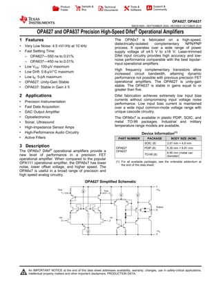
  • 1. Trim 5 Trim 1 +In 3 –In 2 Output 6 7 +VS –VS 4 Product Folder Sample & Buy Technical Documents Tools & Software Support & Community OPA627, OPA637 SBOS165A –SEPTEMBER 2000–REVISED OCTOBER 2015 OPA627 and OPA637 Precision High-Speed Difet® Operational Amplifiers The OPA6x7 is fabricated on a high-speed,1 Features dielectrically-isolated complementary NPN/PNP 1• Very Low Noise: 4.5 nV/√Hz at 10 kHz process. It operates over a wide range of power • Fast Settling Time: supply voltage of ±4.5 V to ±18 V. Laser-trimmed Difet input circuitry provides high accuracy and low-– OPA627—550 ns to 0.01% noise performance comparable with the best bipolar- – OPA637—450 ns to 0.01% input operational amplifiers. • Low VOS: 100-µV maximum High frequency complementary transistors allow • Low Drift: 0.8-µV/°C maximum increased circuit bandwidth, attaining dynamic • Low IB: 5-pA maximum performance not possible with previous precision FET operational amplifiers. The OPA627 is unity-gain• OPA627: Unity-Gain Stable stable. The OPA637 is stable in gains equal to or• OPA637: Stable in Gain ≥ 5 greater than five. Difet fabrication achieves extremely low input bias2 Applications currents without compromising input voltage noise • Precision Instrumentation performance. Low input bias current is maintained • Fast Data Acquisition over a wide input common-mode voltage range with unique cascode circuitry.• DAC Output Amplifier • Optoelectronics The OPA6x7 is available in plastic PDIP, SOIC, and metal TO-99 packages. Industrial and military• Sonar, Ultrasound temperature range models are available.• High-Impedance Sensor Amps • High-Performance Audio Circuitry Device Information(1) • Active Filters PART NUMBER PACKAGE BODY SIZE (NOM) SOIC (8) 3.91 mm × 4.9 mm 3 Description OPA627 PDIP (8) 6.35 mm × 9.81 mm The OPA6x7 Difet® operational amplifiers provide a OPA637 8.95 mm (metal can TO-99 (8)new level of performance in a precision FET diameter) operational amplifier. When compared to the popular (1) For all available packages, see the orderable addendum atOPA111 operational amplifier, the OPA6x7 has lower the end of the data sheet. noise, lower offset voltage, and higher speed. The OPA6x7 is useful in a broad range of precision and high speed analog circuitry. OPA627 Simplified Schematic 1 An IMPORTANT NOTICE at the end of this data sheet addresses availability, warranty, changes, use in safety-critical applications, intellectual property matters and other important disclaimers. PRODUCTION DATA.
  • 2. OPA627, OPA637 SBOS165A –SEPTEMBER 2000–REVISED OCTOBER 2015 www.ti.com Table of Contents 7.5 Device Functional Modes........................................ 191 Features.................................................................. 1 8 Application and Implementation ........................ 202 Applications ........................................................... 1 8.1 Application Information............................................ 203 Description ............................................................. 1 8.2 Typical Application ................................................. 224 Revision History..................................................... 2 9 Power Supply Recommendations...................... 245 Pin Configuration and Functions......................... 3 10 Layout................................................................... 246 Specifications......................................................... 3 10.1 Layout Guidelines ................................................. 246.1 Absolute Maximum Ratings ...................................... 3 10.2 Layout Example .................................................... 256.2 ESD Ratings ............................................................ 4 11 Device and Documentation Support ................. 266.3 Recommended Operating Conditions....................... 4 11.1 Device Support .................................................... 266.4 Thermal Information.................................................. 4 11.2 Documentation Support ....................................... 266.5 Electrical Characteristics........................................... 5 11.3 Related Links ........................................................ 266.6 Typical Characteristics.............................................. 7 11.4 Trademarks........................................................... 267 Detailed Description ............................................ 12 11.5 Electrostatic Discharge Caution............................ 277.1 Overview ................................................................. 12 11.6 Glossary................................................................ 277.2 Functional Block Diagram ....................................... 12 12 Mechanical, Packaging, and Orderable7.3 Feature Description................................................. 12 Information ........................................................... 277.4 Settling Time ........................................................... 19 4 Revision History NOTE: Page numbers for previous revisions may differ from page numbers in the current version. Changes from Original (September 2000) to Revision A Page • Added ESD Ratings table, Feature Description section, Device Functional Modes, Application and Implementation section, Power Supply Recommendations section, Layout section, Device and Documentation Support section, and Mechanical, Packaging, and Orderable Information section. ................................................................................................ 1 • Removed Lead Temperature from Absolute Maximum Ratings table. ................................................................................. 3 2 Submit Documentation Feedback Copyright © 2000–2015, Texas Instruments Incorporated Product Folder Links: OPA627 OPA637
  • 3. Offset Trim –In Output Offset Trim+In –VS +VS No Internal Connection Case connected to –VS. 8 1 2 3 4 5 6 7 Offset Trim –In +In –V No Internal Connection +V Output Offset TrimS S 1 2 3 4 8 7 6 5 OPA627, OPA637 www.ti.com SBOS165A –SEPTEMBER 2000–REVISED OCTOBER 2015 5 Pin Configuration and Functions P and D Packages LMC Package8-Pin PDIP and SOIC 8-Pin TO-99Top View Top View Pin Functions PIN I/O DESCRIPTION NO. NAME 1 Offset Trim — Input offset voltage trim (leave floating if not used) 2 –In I Inverting input 3 +In I Noninverting input 4 –VS — Negative (lowest) power supply 5 Offset Trim — Input offset voltage trim (leave floating if not used) 6 Output O Output 7 +VS — Positive (highest) power supply 8 NC — No internal connection (can be left floating) 6 Specifications 6.1 Absolute Maximum Ratings over operating free-air temperature range (unless otherwise noted) (1) MIN MAX UNIT Supply Voltage ±18 V Input Voltage Range +VS + 2 –VS – 2 V Differential Input Total VS + 4 V Power Dissipation 1000 mW LMC Package –55 125 Operating Temperature °C P, D Package –40 125 LMC Package 175 Junction Temperature °C P, D Package 150 LMC Package –65 150 Storage temperature, Tstg °C P, D Package –40 125 (1) Stresses beyond those listed under Absolute Maximum Ratings may cause permanent damage to the device. These are stress ratings only, which do not imply functional operation of the device at these or any other conditions beyond those indicated under Recommended Operating Conditions. Exposure to absolute-maximum-rated conditions for extended periods may affect device reliability. Copyright © 2000–2015, Texas Instruments Incorporated Submit Documentation Feedback 3 Product Folder Links: OPA627 OPA637
  • 4. OPA627, OPA637 SBOS165A –SEPTEMBER 2000–REVISED OCTOBER 2015 www.ti.com 6.2 ESD Ratings VALUE UNIT OPA627 and OPA637 in PDIP and SOIC Packages Electrostatic V(ESD) Human-body model (HBM), per ANSI/ESDA/JEDEC JS-001(1) ±2500 V discharge OPA627 and OPA637 in SOIC Packages Electrostatic V(ESD) Charged-device model (CDM), per JEDEC specification JESD22-C101(2) ±1000 V discharge (1) JEDEC document JEP155 states that 500-V HBM allows safe manufacturing with a standard ESD control process. (2) JEDEC document JEP157 states that 250-V CDM allows safe manufacturing with a standard ESD control process. 6.3 Recommended Operating Conditions over operating free-air temperature range (unless otherwise noted) MIN NOM MAX UNIT Supply voltage, Vs = (V+) - (V-) 9 (±4.5) 30 (±15) 36 (±18) V P and D packages –25 25 85 °CSpecified temperature LMC package –55 25 125 °C 6.4 Thermal Information OPA627, OPA637 THERMAL METRIC(1) P (DIP) D (SOIC) LMC (TO-99) UNIT 8 PINS 8 PINS 8 PINS RθJA Junction-to-ambient thermal resistance 46.2 107.9 200 °C/W RθJC(top) Junction-to-case (top) thermal resistance 34.5 57.3 — °C/W RθJB Junction-to-board thermal resistance 23.5 49.7 — °C/W ψJT Junction-to-top characterization parameter 11.7 11.7 — °C/W ψJB Junction-to-board characterization parameter 23.3 48.9 — °C/W RθJC(bot) Junction-to-case (bottom) thermal resistance N/A N/A — °C/W (1) For more information about traditional and new thermal metrics, see the Semiconductor and IC Package Thermal Metrics application report, SPRA953. 4 Submit Documentation Feedback Copyright © 2000–2015, Texas Instruments Incorporated Product Folder Links: OPA627 OPA637
  • 5. OPA627, OPA637 www.ti.com SBOS165A –SEPTEMBER 2000–REVISED OCTOBER 2015 6.5 Electrical Characteristics At TA = 25°C, and VS = ±15 V, unless otherwise noted. PARAMETER TEST CONDITIONS MIN TYP MAX UNIT OFFSET VOLTAGE(1) BM, SM grades 40 100 AM grade 130 250 Input offset voltage µV BP grade 100 250 AP, AU grades 280 500 BM, SM grades 0.4 0.8 AM grade 1.2 2 Average drift µV/°C BP grade 0.8 2 AP, AU grades 2.5 BM, BP, SM grades 106 120 Power supply rejection VS = ±4.5 to ±18 V dB AM, AP, AU grades 100 116 INPUT BIAS CURRENT(2) BM, BP, SM grades 1 5 TA = 25°C pA AM, AP, AU grades 2 10 VCM = 0 V BM, BP grades 1 Over specified Input bias current SM grade 50 nA temperature AM, AP, AU grades 2 BM, BP, SM grades 1 VCM = ±10 V, over common-mode voltage pA AM, AP, AU grades 2 BM, BP, SM grades 0.5 5 TA = 25°C pA AM, AP, AU grades 1 10 Input offset current VCM = 0 V BM, BP grades 1 Over specified SM grade 50 nA temperature AM, AP, AU grades 2 NOISE BM, BP, SM grades 15 40 f = 10 Hz AM, AP, AU grades 20 BM, BP, SM grades 8 20 f = 100 Hz AM, AP, AU grades 10 Input voltage noise density nV/√Hz BM, BP, SM grades 5.2 8 f = 1 kHz AM, AP, AU grades 5.6 BM, BP, SM grades 4.5 6 f = 10 kHz AM, AP, AU grades 4.8 BM, BP, SM grades 0.6 1.6 Input voltage noise BW = 0.1 Hz to 10 Hz µVp-p AM, AP, AU grades 0.8 BM, BP, SM grades 1.6 2.5Input bias-current noise f = 100 Hz fA/√Hz density AM, AP, AU grades 2.5 BM, BP, SM grades 30 60 Input bias-current noise BW = 0.1 Hz to 10 Hz fAp-p AM, AP, AU grades 48 INPUT IMPEDANCE Differential Ω || pF1013 || 8 Common-mode Ω || pF1013 || 7 INPUT VOLTAGE RANGE TA = 25°C ±11 ±11.5 Common-mode input range V Over specified temperature ±10.5 ±11 BM, BP, SM grades 106 116 Common-mode rejection VCM = ±10.5 V dB AM, AP, AU grades 100 110 (1) Offset voltage measured fully warmed-up. (2) High-speed test at TJ = 25°C. See Typical Characteristics for warmed-up performance. Copyright © 2000–2015, Texas Instruments Incorporated Submit Documentation Feedback 5 Product Folder Links: OPA627 OPA637
  • 6. OPA627, OPA637 SBOS165A –SEPTEMBER 2000–REVISED OCTOBER 2015 www.ti.com Electrical Characteristics (continued) At TA = 25°C, and VS = ±15 V, unless otherwise noted. PARAMETER TEST CONDITIONS MIN TYP MAX UNIT OPEN-LOOP GAIN BM, BP, SM grades 112 120 TA = 25°C AM, AP, AU grades 106 116 Open-loop voltage gain VO = ±10 V, RL = 1kΩ BM, BP grades 106 117 dB Over specified SM grade 100 114 temperature AM, AP, AU grades 100 110 FREQUENCY RESPONSE G = –1, 10-V step, OPA627 40 55 Slew rate V/µs G = –4, 10-V step, OPA637 100 135 0.01% 550G = –1, 10-V step, OPA627 0.1% 450 Settling time ns 0.01% 450G = –4, 10-V step, OPA637 0.1% 300 G = 1, OPA627 16 Gain-bandwidth product MHz G = 10, OPA637 80 Total harmonic distortion + G = 1, f = 1 kHz 0.00003% noise POWER SUPPLY Specified operating voltage ±15 V Operating voltage range ±4.5 ±18 V Current ±7 ±7.5 mA OUTPUT RL = 1 kΩ ±11.5 ±12.3 Voltage output V Over specified temperature ±11 ±11.5 Current output VO = ±10 V ±45 mA Short-circuit current ±35 ±70/–55 ±100 mA Output impedance, open-loop 1 MHz 55 Ω TEMPERATURE RANGE AP, BP, AM, BM, AU grades –25 85Temperature range °C specification SM grade –55 125 6 Submit Documentation Feedback Copyright © 2000–2015, Texas Instruments Incorporated Product Folder Links: OPA627 OPA637
  • 7. Phase(Degrees) Gain(dB) 30 20 10 0 –10 –90 –120 –150 –180 –210 1 Phase Gain Frequency (MHz) 10 100 75° Phase Margin Phase(Degrees) Gain(dB) 30 20 10 0 –10 –90 –120 –150 –180 –210 1 10 100 Phase Gain Frequency (MHz) Source Resistance ( ) 1k 100 10 1 100 OPA627 + Resistor Resistor Noise Only Spot Noise at 10kHz VoltageNoise(nV/Hz)√ 1k 10k 100k 1M 10M 100M Comparison with OPA27 Bipolar Op Amp + Resistor – + RS Frequency (Hz) VoltageGain(dB) 1 10 100 1k 10k 100k 1M 10M 100M 140 120 100 80 60 40 20 0 –20 OPA637 OPA627 100 10 1 0.1 0.01 1 10 100 1k 10k 100k 1M 10M Bandwidth (Hz) InputVoltageNoise(µV) Noise Bandwidth: 0.1Hz to indicated frequency. RMS p-p 1k 100 10 1 1 Frequency (Hz) VoltageNoise(nV/Hz)√ 10 100 1k 10k 100k 1M 10M OPA627, OPA637 www.ti.com SBOS165A –SEPTEMBER 2000–REVISED OCTOBER 2015 6.6 Typical Characteristics At TA = 25°C, and VS = ±15 V, unless otherwise noted. Figure 1. Input Voltage Noise Spectral Density vs Frequency Figure 2. Total Input Voltage Noise vs Bandwidth Figure 3. Voltage Noise vs Source Resistance Figure 4. Open-Loop Gain vs Frequency Figure 5. OPA627 Gain/Phase vs Frequency Figure 6. OPA637 Gain/Phase vs Frequency Copyright © 2000–2015, Texas Instruments Incorporated Submit Documentation Feedback 7 Product Folder Links: OPA627 OPA637
  • 8. Temperature (°C) CMRandPSR(dB) 125 120 115 110 105 –75 PSR CMR –50 –25 0 25 50 75 100 125 Frequency (Hz) Power-SupplyRejection(dB) 140 120 100 80 60 40 20 0 1 –VS PSRR 627 and 637 +VS PSRR 627 637 10 100 1k 10k 100k 1M 10M Frequency (Hz) Common-ModeRejectionRatio(dB) 140 120 100 80 60 40 20 0 1 10 100 1k 10k 100k 1M 10M OPA627 OPA637 130 120 110 100 90 80 Common-ModeRejection(dB) Common-Mode Voltage (V) –15 –10 –5 0 5 10 15 VoltageGain(dB) Temperature (°C) 125 120 115 110 105 –75 –50 –25 0 25 50 75 100 125 Frequency (Hz) OutputResistance() 100 80 60 40 20 0 2 20 200 2k 20k 200k 2M 20M OPA627, OPA637 SBOS165A –SEPTEMBER 2000–REVISED OCTOBER 2015 www.ti.com Typical Characteristics (continued) At TA = 25°C, and VS = ±15 V, unless otherwise noted. Figure 8. Open-Loop Output Impedance vs FrequencyFigure 7. Open-Loop Gain vs Temperature Figure 9. Common-Mode Rejection vs Frequency Figure 10. Common-Mode Rejection vs Input Common-Mode Voltage Figure 11. Power-Supply Rejection vs Frequency Figure 12. Power-Supply Rejection and Common-Mode Rejection vs Temperature 8 Submit Documentation Feedback Copyright © 2000–2015, Texas Instruments Incorporated Product Folder Links: OPA627 OPA637
  • 9. Frequency (Hz) THD+N(%) 20 100 1k 10k 20k 0.1 0.01 0.001 0.0001 0.00001 G = +10 G = +1 Measurement BW: 80kHz – + – + 100pF 100pF G = +1 G = +10 VI VI 549 5k 600600 V = ±10VO V = ±10VO Frequency (Hz) THD+N(%) 20 100 1k 10k 20k 1 0.1 0.01 0.001 0.0001 G = +10 G = +50 – + 100pF G = +10 VI 549 5k 600 V = ±10VO – + 100pF G = +50 VI 102 5k 600 V = ±10VO Measurement BW: 80kHz Temperature (°C) Gain-Bandwidth(MHz) 24 20 16 12 8 –75 Slew Rate GBW 60 55 50 SlewRate(V/µs) –50 –25 0 25 50 75 100 125 Temperature (°C) Gain-Bandwidth(MHz) 120 100 80 60 40 –75 SlewRate(V/µs) 160 140 120 100 80 Slew Rate GBW –50 –25 0 25 50 75 100 125 Temperature (°C) SupplyCurrent(mA) 8 7.5 7 6.5 6 –75 –50 –25 0 25 50 75 100 125 OutputCurrent(mA) 100 80 60 40 20 0 –75 –50 –25 0 25 50 75 100 125 Temperature (°C) –IL at VO = –10V –IL at VO = 0V +IL at VO = +10V +IL at VO = 0V OPA627, OPA637 www.ti.com SBOS165A –SEPTEMBER 2000–REVISED OCTOBER 2015 Typical Characteristics (continued) At TA = 25°C, and VS = ±15 V, unless otherwise noted. Figure 13. Supply Current vs Temperature Figure 14. Output Current Limit vs Temperature Figure 15. OPA627 Gain-Bandwidth and Slew Rate vs Figure 16. OPA637 Gain-Bandwidth and Slew Rate vs Temperature Temperature Figure 17. OPA627 Total Harmonic Distortion + Noise vs Figure 18. OPA637 Total Harmonic Distortion + Noise vs Frequency Frequency Copyright © 2000–2015, Texas Instruments Incorporated Submit Documentation Feedback 9 Product Folder Links: OPA627 OPA637
  • 10. Frequency (Hz) OutputVoltage(Vp-p) 30 20 10 0 100k 1M 10M 100M OPA627 OPA637 100 10 1 0.1 –1 –10 –100 –1000 Closed-Loop Gain (V/V) SettlingTime(µs) Error Band: ±0.01% OPA637 OPA627 Time From Power Turn-On (Min) OffsetVoltageChange(µV) 50 25 0 –25 –50 0 1 2 3 4 5 6 Common-Mode Voltage (V) InputBiasCurrentMultiplier 1.2 1.1 1 0.9 0.8 –15 –10 –5 0 5 10 15 Beyond Linear Common-Mode Range Beyond Linear Common-Mode Range Junction Temperature (°C) InputCurrent(pA) 10k 1k 100 10 1 0.1 –50 –25 0 25 50 75 100 125 150 IB IOS Supply Voltage (±VS) InputBiasCurrent(pA) 20 15 10 5 0 ±4 ±6 ±8 ±10 ±12 ±14 ±16 ±18 NOTE: Measured fully warmed-up. TO-99 with 0807HS Heat Sink TO-99 Plastic DIP, SOIC OPA627, OPA637 SBOS165A –SEPTEMBER 2000–REVISED OCTOBER 2015 www.ti.com Typical Characteristics (continued) At TA = 25°C, and VS = ±15 V, unless otherwise noted. Figure 19. Input Bias and Offset Current vs Junction Figure 20. Input Bias Current vs Power Supply Voltage Temperature Figure 21. Input Bias Current vs Common-Mode Voltage Figure 22. Input Offset Voltage Warm-up vs Time Figure 24. Settling Time vs Closed-Loop GainFigure 23. Maximum Output Voltage vs Frequency 10 Submit Documentation Feedback Copyright © 2000–2015, Texas Instruments Incorporated Product Folder Links: OPA627 OPA637
  • 11. 1500 1000 500 0 0.001 0.01 0.1 1 10 Error Band (%) SettlingTime(ns) OPA637 G = –4 OPA627 G = –1 – + CF RI RF 2k +5V –5V OPA627 OPA637 RI 2k 500 RF 2k 2k CF 6pF 4pF 0 150 200 300 400 500 Load Capacitance (pF) 3 2 1 0 SettlingTime(µs) Error Band: ±0.01% OPA637 G = –4 OPA627 G = –1 OPA627, OPA637 www.ti.com SBOS165A –SEPTEMBER 2000–REVISED OCTOBER 2015 Typical Characteristics (continued) At TA = 25°C, and VS = ±15 V, unless otherwise noted. Figure 25. Settling Time vs Error Band Figure 26. Settling Time vs Load Capacitance Copyright © 2000–2015, Texas Instruments Incorporated Submit Documentation Feedback 11 Product Folder Links: OPA627 OPA637
  • 12. Trim 5 Trim 1 +In 3 –In 2 Output 6 7 +VS –VS 4 OPA627, OPA637 SBOS165A –SEPTEMBER 2000–REVISED OCTOBER 2015 www.ti.com 7 Detailed Description 7.1 Overview The OPA6x7 Difet operational amplifiers provide a new level of performance in a precision FET operational amplifier. When compared to the popular OPA111 operational amplifier, the OPA6x7 has lower noise, lower offset voltage, and higher speed. The OPA6x7 is useful in a broad range of precision and high speed analog circuitry. The OPA6x7 is fabricated on a high-speed, dielectrically-isolated complementary NPN/PNP process. It operates over a wide range of power supply voltage of ±4.5 V to ±18 V. Laser-trimmed Difet input circuitry provides high accuracy and low-noise performance comparable with the best bipolar-input operational amplifiers. High frequency complementary transistors allow increased circuit bandwidth, attaining dynamic performance not possible with previous precision FET operational amplifiers. The OPA627 is unity-gain stable. The OPA637 is stable in gains equal to or greater than five. Difet fabrication achieves extremely low input bias currents without compromising input voltage noise performance. Low input bias current is maintained over a wide input common-mode voltage range with unique cascode circuitry. The OPA6x7 is available in plastic PDIP, SOIC, and metal TO-99 packages. Industrial and military temperature range models are available. 7.2 Functional Block Diagram 7.3 Feature Description The OPA627 is unity-gain stable. The OPA637 may achieve higher speed and bandwidth in circuits with noise gain greater than five. Noise gain refers to the closed-loop gain of a circuit, as if the noninverting operational amplifier input were being driven. For example, the OPA637 may be used in a noninverting amplifier with gain greater than five, or an inverting amplifier of gain greater than four. When choosing between the OPA627 or OPA637, consider the high frequency noise gain of your circuit configuration. Circuits with a feedback capacitor (see Figure 27) place the operational amplifier in unity noise- gain at high frequency. These applications must use the OPA627 for proper stability. An exception is the circuit in Figure 28, where a small feedback capacitance is used to compensate for the input capacitance at the inverting input of the operational amplifier. In this case, the closed-loop noise gain remains constant with frequency, so if the closed-loop gain is equal to five or greater, the OPA637 may be used. 12 Submit Documentation Feedback Copyright © 2000–2015, Texas Instruments Incorporated Product Folder Links: OPA627 OPA637
  • 13. – + C2 C1 R2 R1 OPA637 C1 = CIN + CSTRAY C2 = R1 C1 R2 – + – + – + – + – + – + Buffer Bandwidth Limiting Integrator Filter RI RF < 4R Inverting Amp G < |–4| RI RF < 4RI Non-Inverting Amp G < 5 OPA627 OPA627 OPA627OPA627 OPA627 OPA627 OPA627, OPA637 www.ti.com SBOS165A –SEPTEMBER 2000–REVISED OCTOBER 2015 Feature Description (continued) Figure 27. Circuits With Noise Gain Less Than Five Require the OPA627 for Proper Stability Figure 28. Circuits With Noise Gain Equal to or Greater Than Five May Use the OPA637 7.3.1 Offset Voltage Adjustment The OPA6x7 is laser-trimmed for low offset voltage and drift, so many circuits will not require external adjustment. Figure 29 shows the optional connection of an external potentiometer to adjust offset voltage. This adjustment should not be used to compensate for offsets created elsewhere in a system (such as in later amplification stages or in an A/D converter), because this could introduce excessive temperature drift. Generally, the offset drift will change by approximately 4 µV/°C for 1 mV of change in the offset voltage due to an offset adjustment (as shown in Figure 29). Copyright © 2000–2015, Texas Instruments Incorporated Submit Documentation Feedback 13 Product Folder Links: OPA627 OPA637
  • 14. – + 2 3 7 1 5 6 +VS –VS OPA627/637 100k 10k to 1M Potentiometer (100k preferred) ±10mV Typical Trim Range 4 OPA627, OPA637 SBOS165A –SEPTEMBER 2000–REVISED OCTOBER 2015 www.ti.com Feature Description (continued) Figure 29. Optional Offset Voltage Trim Circuit 7.3.2 Noise Performance Some bipolar operational amplifiers may provide lower voltage noise performance, but both voltage noise and bias current noise contribute to the total noise of a system. The OPA6x7 provides both low voltage noise and low current noise. This provides optimum noise performance over a wide range of sources, including reactive-source impedances. This can be seen in the performance curve showing the noise of a source resistor combined with the noise of an OPA627. Above a 2-kΩ source resistance, the operational amplifier contributes little additional noise. Below 1 kΩ, operational amplifier noise dominates over the resistor noise, but compares favorably with precision bipolar operational amplifiers. 7.3.3 Input Bias Current Difet fabrication of the OPA6x7 provides low input bias current. Because the gate current of a FET doubles approximately every 10°C, to achieve lowest input bias current, keep the die temperature as low as possible. The high speed, and therefore higher quiescent current, of the OPA6x7 can lead to higher chip temperature. A simple press-on heat sink such as the Burr-Brown model 807HS (TO-99 metal package) can reduce chip temperature by approximately 15°C, lowering the IB to one-third its warmed-up value. The 807HS heat sink can also reduce low-frequency voltage noise caused by air currents and thermoelectric effects. See the data sheet on the 807HS for details. Temperature rise in the plastic PDIP and SOIC packages can be minimized by soldering the device to the circuit board. Wide copper traces also help dissipate heat. The OPA6x7 may also be operated at reduced power supply voltage, to minimize power dissipation and temperature rise. Using ±5-V power supplies reduces power dissipation to one-third of that at ±15 V. This reduces the IB of TO- 99 metal package devices to approximately one-fourth the value at ±15 V. Leakage currents between printed-circuit-board traces can easily exceed the input bias current of the OPA6x7. A circuit board guard pattern (see Figure 30) reduces leakage effects. By surrounding critical high impedance input circuitry with a low impedance circuit connection at the same potential, leakage current will flow harmlessly to the low-impedance node. The case (TO-99 metal package only) is internally connected to –VS. Input bias current may also be degraded by improper handling or cleaning. Contamination from handling parts and circuit boards may be removed with cleaning solvents and deionized water. Each rinsing operation should be followed by a 30-minute bake at 85°C. Many FET-input operational amplifiers exhibit large changes in input bias current with changes in input voltage. Input stage cascode circuitry makes the input bias current of the OPA6x7 virtually constant with wide common- mode voltage changes. This is ideal for accurate, high input-impedance buffer applications. 14 Submit Documentation Feedback Copyright © 2000–2015, Texas Instruments Incorporated Product Folder Links: OPA627 OPA637
  • 15. +VS 5k (2) HP 5082-2811 1k 5k –VS VO Diode Bridge BB: PWS740-3 ZD : 10V IN9611 Clamps output at VO = ±11.5V RI VI – + RF ZD1 OPA627 B. Board Layout for Input Guarding: Guard top and bottom of board. Alternate—use Teflon® standoff for sen- sitive input pins. Teflon® E.I. du Pont de Nemours & Co. – + 2 3In Non-inverting 6 OPA627 Out – + 2 3 In Inverting 6 OPA627 Out – + 2 3In Buffer 6 OPA627 Out 3 2 4 5 6 7 8 No Internal Connection 1 TO-99 Bottom View To Guard Drive OPA627, OPA637 www.ti.com SBOS165A –SEPTEMBER 2000–REVISED OCTOBER 2015 Feature Description (continued) Figure 30. Connection of Input Guard for Lowest IB 7.3.4 Phase-Reversal Protection The OPA6x7 has internal phase-reversal protection. Many FET-input operational amplifiers exhibit a phase reversal when the input is driven beyond its linear common-mode range. This is most often encountered in noninverting circuits when the input is driven below –12 V, causing the output to reverse into the positive rail. The input circuitry of the OPA6x7 does not induce phase reversal with excessive common-mode voltage, so the output limits into the appropriate rail. 7.3.5 Output Overload When the inputs to the OPA6x7 are overdriven, the output voltage of the OPA6x7 smoothly limits at approximately 2.5 V from the positive and negative power supplies. If driven to the negative swing limit, recovery takes approximately 500 ns. When the output is driven into the positive limit, recovery takes approximately 6 µs. Output recovery of the OPA627 can be improved using the output clamp circuit shown in Figure 31. Placing diodes at the inverting input prevent degradation of input bias current. Figure 31. Clamp Circuit for Improved Overload Recovery Copyright © 2000–2015, Texas Instruments Incorporated Submit Documentation Feedback 15 Product Folder Links: OPA627 OPA637
  • 16. R1 – + RF 1k OPA627 CF G = +1 BW 1MHz 200pF For Approximate Butterworth Response: CF = 2 RO CL RF RF >> RO G = 1+ RF R1 ≥ Optional Gain Gain > 1 f–3dB = 1 2p R√ F RO CF CL CL 5nF RO 20 OPA627, OPA637 SBOS165A –SEPTEMBER 2000–REVISED OCTOBER 2015 www.ti.com Feature Description (continued) 7.3.6 Capacitive Loads As with any high-speed operational amplifier, best dynamic performance can be achieved by minimizing the capacitive load. Because a load capacitance presents a decreasing impedance at higher frequency, a load capacitance which is easily driven by a slow operational amplifier can cause a high-speed operational amplifier to perform poorly. See the typical curves showing settling times as a function of capacitive load. The lower bandwidth of the OPA627 makes it the better choice for driving large capacitive loads. Figure 32 shows a circuit for driving very large load capacitance. The two-pole response of this circuit can also be used to sharply limit system bandwidth, often useful in reducing the noise of systems which do not require the full bandwidth of the OPA627. Figure 32. Driving Large Capacitive Loads 7.3.7 Input Protection The inputs of the OPA6x7 are protected for voltages from +VS + 2 V to –VS – 2 V. If the input voltage can exceed these limits, the amplifier should be protected. The diode clamps shown in (a) in Figure 33 prevent the input voltage from exceeding one forward diode voltage drop beyond the power supplies, which is well within the safe limits. If the input source can deliver current in excess of the maximum forward current of the protection diodes, use a series resistor, RS, to limit the current. Be aware that adding resistance to the input increases noise. The 4- nV/√Hz theoretical thermal noise of a 1-kΩ resistor will add to the 4.5-nV/√Hz noise of the OPA6x7 (by the square-root of the sum of the squares), producing a total noise of 6 nV/√Hz. Resistors less than 100 Ω add negligible noise. Leakage current in the protection diodes can increase the total input bias current of the circuit. The specified maximum leakage current for commonly used diodes such as the 1N4148 is approximately 25 nA, more than a thousand times larger than the input bias current of the OPA6x7. Leakage current of these diodes is typically much lower and may be adequate in many applications. Light falling on the junction of the protection diodes can dramatically increase leakage current, so common glass-packaged diodes should be shielded from ambient light. Very low leakage can be achieved by using a diode-connected FET as shown. The 2N4117A is specified at 1 pA and its metal case shields the junction from light. Sometimes input protection is required on I/V converters of inverting amplifiers; see (b) in Figure 33. Although in normal operation, the voltage at the summing junction will be near zero (equal to the offset voltage of the amplifier), and large input transients may cause this node to exceed 2 V beyond the power supplies. In this case, the summing junction should be protected with diode clamps connected to ground. Even with the low voltage present at the summing junction, common signal diodes may have excessive leakage current. Because the reverse voltage on these diodes is clamped, a diode-connected signal transistor can act as an inexpensive low leakage diode; see (b) in Figure 33. 16 Submit Documentation Feedback Copyright © 2000–2015, Texas Instruments Incorporated Product Folder Links: OPA627 OPA637
  • 17. – + –VS +VS Optional RS VO D: IN4148 — 25nA Leakage 2N4117A — 1pA Leakage (a) = – + IIN VO D D D (b) D D: 2N3904 = NC Siliconix OPA627 OPA627 OPA627, OPA637 www.ti.com SBOS165A –SEPTEMBER 2000–REVISED OCTOBER 2015 Feature Description (continued) Figure 33. Input Protection Circuits 7.3.8 EMI Rejection Ratio (EMIRR) The electromagnetic interference (EMI) rejection ratio, or EMIRR, describes the EMI immunity of operational amplifiers. An adverse effect that is common to many operational amplifiers is a change in the offset voltage as a result of RF signal rectification. An operational amplifier that is more efficient at rejecting this change in offset as a result of EMI has a higher EMIRR and is quantified by a decibel value. Measuring EMIRR can be performed in many ways, but this report provides the EMIRR IN+, which specifically describes the EMIRR performance when the RF signal is applied to the noninverting input pin of the operational amplifier. In general, only the noninverting input is tested for EMIRR for the following three reasons: • Operational amplifier input pins are known to be the most sensitive to EMI, and typically rectify RF signals better than the supply or output pins. • The noninverting and inverting operational amplifier inputs have symmetrical physical layouts and exhibit nearly matching EMIRR performance. • EMIRR is easier to measure on noninverting pins than on other pins because the noninverting input terminal can be isolated on a printed-circuit-board (PCB). This isolation allows the RF signal to be applied directly to the noninverting input terminal with no complex interactions from other components or connecting PCB traces. A more formal discussion of the EMIRR IN+ definition and test method is provided in application report EMI Rejection Ratio of Operational Amplifiers (SBOA128), available for download at www.ti.com. The EMIRR IN+ of the OPA627 is plotted versus frequency as shown in Figure 34. If available, any dual and quad operational amplifier device versions have nearly similar EMIRR IN+ performance. The OPA627 unity-gain bandwidth is 16 MHz. EMIRR performance below this frequency denotes interfering signals that fall within the operational amplifier bandwidth. Copyright © 2000–2015, Texas Instruments Incorporated Submit Documentation Feedback 17 Product Folder Links: OPA627 OPA637
  • 18. Frequency (MHz) EMIRRIN+(db) 0 20 40 60 80 100 120 140 10M 100M 1G 10G PRF = -10 dbm VS = r15 V VCM = 0 V OPA627, OPA637 SBOS165A –SEPTEMBER 2000–REVISED OCTOBER 2015 www.ti.com Feature Description (continued) Figure 34. OPA627 EMIRR IN+ vs Frequency Table 1 shows the EMIRR IN+ values for the OPA627 at particular frequencies commonly encountered in real- world applications. Applications listed in Table 1 may be centered on or operated near the particular frequency shown. This information may be of special interest to designers working with these types of applications, or working in other fields likely to encounter RF interference from broad sources, such as the industrial, scientific, and medical (ISM) radio band. Table 1. OPA627 EMIRR IN+ for Frequencies of Interest FREQUENCY APPLICATION / ALLOCATION EMIRR IN+ 400 MHz Mobile radio, mobile satellite/space operation, weather, radar, UHF 46.2 dB GSM, radio com/nav./GPS (to 1.6 GHz), ISM, aeronautical mobile, 900 MHz 60.3 dB UHF 1.8 GHz GSM, mobile personal comm. broadband, satellite, L-band 81 dB 802.11b/g/n, Bluetooth™, mobile personal comm., ISM, amateur 2.4 GHz 96.9 dB radio/satellite, S-band 3.6 GHz Radiolocation, aero comm./nav., satellite, mobile, S-band 108.9 dB 802.11a/n, aero comm./nav., mobile comm., space/satellite 5 Ghz 116.8 dB operation, C-band 7.3.8.1 EMIRR IN+ Test Configuration Figure 35 shows the circuit configuration for testing the EMIRR IN+. An RF source is connected to the operational amplifier noninverting input terminal using a transmission line. The operational amplifier is configured in a unity gain buffer topology with the output connected to a low-pass filter (LPF) and a digital multimeter (DMM). A large impedance mismatch at the operational amplifier input causes a voltage reflection; however, this effect is characterized and accounted for when determining the EMIRR IN+. The resulting DC offset voltage is sampled and measured by the multimeter. The LPF isolates the multimeter from residual RF signals that may interfere with multimeter accuracy. Refer to SBOA128 for more details. 18 Submit Documentation Feedback Copyright © 2000–2015, Texas Instruments Incorporated Product Folder Links: OPA627 OPA637
  • 19. OPA627 OPA637 RI, R1 2k 500 CF 6pF 4pF Error Band ±0.5mV ±0.2mV (0.01%) NOTE: CF is selected for best settling time performance depending on test fixture layout. Once optimum value is determined, a fixed capacitor may be used. – + ±5V Out +15V 2k CF 2kW Error Out RI RI 51 –15V HP- 5082- 2835 High Quality Pulse Generator / + ± Low-Pass Filter50 Digital Multimeter Ambient temperature: 25Û& Sample / Averaging +VS -VS Not shown: 0.1 µF and 10 µF supply decoupling RF source DC Bias: 0 V Modulation: None (CW) Frequency Sweep: 201 pt. Log OPA627, OPA637 www.ti.com SBOS165A –SEPTEMBER 2000–REVISED OCTOBER 2015 Figure 35. EMIRR IN+ Test Configuration Schematic 7.4 Settling Time The OPA627 and OPA637 have fast settling times, as low as 300 ns. Figure 36 illustrates the circuit used to measure settling time for the OPA627 and OPA637. Figure 36. Settling Time and Slew Rate Test Circuit 7.5 Device Functional Modes The OPA627 and OPA6377 have a single functional mode and are operational when the power-supply voltage is greater than 9V (±4.5 V). The maximum power supply voltage for the OPA627 and OPA637 are 36 V (±18 V). Copyright © 2000–2015, Texas Instruments Incorporated Submit Documentation Feedback 19 Product Folder Links: OPA627 OPA637
  • 20. This composite amplifier uses the OPA603 current-feedback op amp to provide extended bandwidth and slew rate at high closed-loop gain. The feedback loop is closed around the composite amp, preserving the precision input characteristics of the OPA627/637. Use separate power supply bypass capacitors for each op amp. GAIN A1 R1 R2 R3 R4 –3dB SLEW RATE (V/V) OP AMP (W ) (k ) ( ) (k ) (MHz) (V/µs) 100 OPA627 50.5(1) 4.99 20 1 15 700 1000 OPA637 49.9 4.99 12 1 11 500 NOTE: (1) Closest 1/2% value. ∗Minimize capacitance at this node.+ – OPA603 – + A1 R3 R1 R4 R2 VI VO * RL ‡ 150 for ±10V Out –In +In + – OPA637 Differential Voltage Gain = (1 + 2RF/RG) • 10 2 3 – + – + INA106 Differential Amplifier 1 6 5 Output Gain = 1000 CMRR 116dB Bandwidth 400kHz OPA637 10k 10k 100k 100k Input Common-Mode Range = ±10V » » 3pF RF 5k RF 5k RG 101 –In +In + – OPA637 Differential Voltage Gain = 1 + 2RF/RG 2 3 – + – + INA105 Differential Amplifier 1 6 5 Output Gain = 100 CMRR 116dB Bandwidth 1MHz OPA637 25k 25k 25k 25k Input Common-Mode Range = ±5V » » 3pF RF 5k RF 5kW RG 101 OPA627, OPA637 SBOS165A –SEPTEMBER 2000–REVISED OCTOBER 2015 www.ti.com 8 Application and Implementation NOTE Information in the following applications sections is not part of the TI component specification, and TI does not warrant its accuracy or completeness. TI’s customers are responsible for determining suitability of components for their purposes. Customers should validate and test their design implementation to confirm system functionality. 8.1 Application Information The OPA627 and OPA637 are ideally suited to use as input amplifiers in instrumentation amplifier configurations requiring high speed, fast settling and high input impedance. Figure 37. High Speed Instrumentation Amplifier, Gain = 100 Figure 38. High Speed Instrumentation Amplifier, Gain = 1000 Figure 39. Composite Amplifier for Wide Bandwidth 20 Submit Documentation Feedback Copyright © 2000–2015, Texas Instruments Incorporated Product Folder Links: OPA627 OPA637
  • 21. When driven with a very fast input step (left), common-mode transients cause a slight variation in input stage currents which will reduce output slew rate. If the input step slew rate is reduced (right), output slew rate will increase slightly. NOTE: (1) Optimum value will depend on circuit board lay- out and stray capacitance at the inverting input. LARGE SIGNAL RESPONSE +10 0 –10 VOUT(V) +10 0 –10 (C) (D) VOUT(V) – + OPA627 G = –1 2k 2k 6pF(1) VOUT FPO When used as a unity-gain buffer, large common-mode input voltage steps produce transient variations in input-stage currents. This causes the rising edge to be slower and falling edges to be faster than nominal slew rates observed in higher-gain circuits. (A) (B) SMALL SIGNAL RESPONSELARGE SIGNAL RESPONSE – + OPA627 G = 1 OPA627, OPA637 www.ti.com SBOS165A –SEPTEMBER 2000–REVISED OCTOBER 2015 Application Information (continued) Figure 40. OPA627 Dynamic Performance, G = 1 Figure 41. OPA627 Dynamic Performance, G = –1 Copyright © 2000–2015, Texas Instruments Incorporated Submit Documentation Feedback 21 Product Folder Links: OPA627 OPA637
  • 22. 1 3 2 5 2 2 1 3 4 3 4 2 5 1 R R C COutput s Input s s C 1 R 1 R 1 R 1 R R C C + ± OPA627 Output Input R1 590 R4 2.94 k R3 499 C2 39 nF C5 1 nF OPA637 LARGE SIGNAL RESPONSE OPA637 SMALL SIGNAL RESPONSE FPO –10 0 +10 –100 0 +100 (F)(E) – + OPA637 G = 5 2k 500 4pF(1) VOUT NOTE: (1) Optimum value will depend on circuit board layout and capacitance at inverting input. VOUT(V) VOUT(mV) OPA627, OPA637 SBOS165A –SEPTEMBER 2000–REVISED OCTOBER 2015 www.ti.com Application Information (continued) Figure 42. OPA637 Dynamic Response, G = 5 8.2 Typical Application Low pass filters are commonly employed in signal processing applications to reduce noise and prevent aliasing. The OPA627 and OPA637 are ideally suited to construct high speed, high precision active filters. Figure 43 illustrates a second order low pass filter commonly encountered in signal processing applications. Figure 43. Second Order Low Pass Filter 8.2.1 Design Requirements Use the following parameters for this design example: • Gain = 5 V/V (inverting gain) • Low pass cutoff frequency = 25 kHz • Second order Chebyshev filter response with 3-dB gain peaking in the passband 8.2.2 Detailed Design Procedure The infinite-gain multiple-feedback circuit for a low-pass network function is shown in Figure 43. Use Equation 1 to calculate the voltage transfer function. (1) 22 Submit Documentation Feedback Copyright © 2000–2015, Texas Instruments Incorporated Product Folder Links: OPA627 OPA637
  • 23. Frequency (Hz) Gain(db) -60 -40 -20 0 20 100 1k 10k 100k 1M 4 1 C 3 4 2 5 R Gain R 1 f 1 R R C C 2S OPA627, OPA637 www.ti.com SBOS165A –SEPTEMBER 2000–REVISED OCTOBER 2015 Typical Application (continued) This circuit produces a signal inversion. For this circuit the gain at DC and the low pass cutoff frequency can be calculated using Equation 2. (2) Software tools are readily available to simplify filter design. WEBENCH® Filter Designer is a simple, powerful, and easy-to-use active filter design program. The WEBENCH Filter Designer lets you create optimized filter designs using a selection of TI operational amplifiers and passive components from TI's vendor partners. Available as a web based tool from the WEBENCH® Design Center, WEBENCH® Filter Designer allows you to design, optimize, and simulate complete multi-stage active filter solutions within minutes. 8.2.3 Application Curve Figure 44. OPA627 2nd Order 25 kHz, Chebyshev, Low Pass Filter Copyright © 2000–2015, Texas Instruments Incorporated Submit Documentation Feedback 23 Product Folder Links: OPA627 OPA637
  • 24. OPA627, OPA637 SBOS165A –SEPTEMBER 2000–REVISED OCTOBER 2015 www.ti.com 9 Power Supply Recommendations The OPA627 and OPA637 are specified for operation from 9 V to 36 V (±4.5 V to ±18 V); many specifications apply from –25°C to 85°C (P and D packages) and –55°C to 125°C (LMC package). Parameters that can exhibit significant variance with regard to operating voltage or temperature are presented in the Typical Characteristics. 10 Layout 10.1 Layout Guidelines For best operational performance of the device, use good PCB layout practices, including: • Noise can propagate into analog circuitry through the power pins of the circuit as a whole and operational amplifier itself. Bypass capacitors are used to reduce the coupled noise by providing low-impedance power sources local to the analog circuitry. – Connect low-ESR, 0.1-µF ceramic bypass capacitors between each supply pin and ground, placed as close to the device as possible. A single bypass capacitor from V+ to ground is applicable for single- supply applications. – The OPA6x7 is capable of high-output current (in excess of 45 mA). Applications with low impedance loads or capacitive loads with fast transient signals demand large currents from the power supplies. Larger bypass capacitors such as 1-µF solid tantalum capacitors may improve dynamic performance in these applications. • Separate grounding for analog and digital portions of circuitry is one of the simplest and most-effective methods of noise suppression. One or more layers on multilayer PCBs are usually devoted to ground planes. A ground plane helps distribute heat and reduces EMI noise pickup. Make sure to physically separate digital and analog grounds paying attention to the flow of the ground current. For more detailed information refer to Circuit Board Layout Techniques (SLOA089). • To reduce parasitic coupling, run the input traces as far away from the supply or output traces as possible. If these traces cannot be kept separate, crossing the sensitive trace perpendicular is much better as opposed to in parallel with the noisy trace. • Place the external components as close to the device as possible. As shown in Figure 45, keeping RF and RG close to the inverting input minimizes parasitic capacitance. • Keep the length of input traces as short as possible. Always remember that the input traces are the most sensitive part of the circuit. • Consider a driven, low-impedance guard ring around the critical traces. A guard ring can significantly reduce leakage currents from nearby traces that are at different potentials. • The case (TO-99 metal package only) is internally connected to the negative power supply, as with most common operational amplifiers. • Pin 8 of the plastic PDIP, SOIC, and TO-99 packages has no internal connection. • Cleaning the PCB following board assembly is recommended for best performance. • Any precision integrated circuit may experience performance shifts due to moisture ingress into the plastic package. Following any aqueous PCB cleaning process, baking the PCB assembly is recommended to remove moisture introduced into the device packaging during the cleaning process. A low temperature, post cleaning bake at 85°C for 30 minutes is sufficient for most circumstances. 24 Submit Documentation Feedback Copyright © 2000–2015, Texas Instruments Incorporated Product Folder Links: OPA627 OPA637
  • 25. B. Board Layout for Input Guarding: Guard top and bottom of board. Alternate—use Teflon® standoff for sen- sitive input pins. Teflon® E.I. du Pont de Nemours & Co. – + 2 3In Non-inverting 6 OPA627 Out – + 2 3 In Inverting 6 OPA627 Out – + 2 3In Buffer 6 OPA627 Out 3 2 4 5 6 7 8 No Internal Connection 1 TO-99 Bottom View To Guard Drive Offset trim ±IN +IN V± V+ OUTPUT NC Offset trim VS+ GND VS± GND Ground (GND) plane on another layer VOUT VIN GND Run the input traces as far away from the supply lines as possible Use low-ESR, ceramic bypass capacitor RF RG Place components close to device and to each other to reduce parasitic errors +VIN VOUTRG RF (Schematic Representation) Use low-ESR, ceramic bypass capacitor OPA627, OPA637 www.ti.com SBOS165A –SEPTEMBER 2000–REVISED OCTOBER 2015 10.2 Layout Example Figure 45. OPA627 Layout Example for the Noninverting Configuration Figure 46. Board Layout for Input Guarding (LMC Package) Copyright © 2000–2015, Texas Instruments Incorporated Submit Documentation Feedback 25 Product Folder Links: OPA627 OPA637
  • 26. OPA627, OPA637 SBOS165A –SEPTEMBER 2000–REVISED OCTOBER 2015 www.ti.com 11 Device and Documentation Support 11.1 Device Support 11.1.1 Development Support 11.1.1.1 TINA-TI™ (Free Software Download) TINA™ is a simple, powerful, and easy-to-use circuit simulation program based on a SPICE engine. TINA-TI is a free, fully-functional version of the TINA software, preloaded with a library of macro models in addition to a range of both passive and active models. TINA-TI provides all the conventional dc, transient, and frequency domain analysis of SPICE, as well as additional design capabilities. Available as a free download from the Analog eLab Design Center, TINA-TI offers extensive post-processing capability that allows users to format results in a variety of ways. Virtual instruments offer the ability to select input waveforms and probe circuit nodes, voltages, and waveforms, creating a dynamic quick-start tool. WEBENCH® Filter Designer is a simple, powerful, and easy-to-use active filter design program. The WEBENCH Filter Designer lets you create optimized filter designs using a selection of TI operational amplifiers and passive components from TI's vendor partners. Available as a web based tool from the WEBENCH® Design Center, WEBENCH® Filter Designer allows you to design, optimize, and simulate complete multi-stage active filter solutions within minutes. NOTE These files require that either the TINA software (from DesignSoft™) or TINA-TI software be installed. Download the free TINA-TI software from the TINA-TI folder. 11.1.1.2 TI Precision Designs The OPA627 is featured in several TI Precision Designs, available online at http://www.ti.com/ww/en/analog/precision-designs/. TI Precision Designs are analog solutions created by TI’s precision analog applications experts and offer the theory of operation, component selection, simulation, complete PCB schematic and layout, bill of materials, and measured performance of many useful circuits. 11.2 Documentation Support 11.2.1 Related Documentation For related documentation see the following: • Circuit Board Layout Techniques, SLOA089. • Op Amps for Everyone, SLOD006. • Compensate Transimpedance Amplifiers Intuitively, SBOS055. • Noise Analysis for High Speed op Amps, SBOA066. 11.3 Related Links The table below lists quick access links. Categories include technical documents, support and community resources, tools and software, and quick access to sample or buy. Table 2. Related Links TECHNICAL TOOLS & SUPPORT & PARTS PRODUCT FOLDER SAMPLE & BUY DOCUMENTS SOFTWARE COMMUNITY OPA627 Click here Click here Click here Click here Click here OPA637 Click here Click here Click here Click here Click here 11.4 Trademarks TINA-TI is a trademark of Texas Instruments, Inc and DesignSoft, Inc. Difet is a registered trademark of Texas Instruments. TINA, DesignSoft are trademarks of DesignSoft, Inc. 26 Submit Documentation Feedback Copyright © 2000–2015, Texas Instruments Incorporated Product Folder Links: OPA627 OPA637
  • 27. OPA627, OPA637 www.ti.com SBOS165A –SEPTEMBER 2000–REVISED OCTOBER 2015 11.4 Trademarks (continued) All other trademarks are the property of their respective owners. 11.5 Electrostatic Discharge Caution These devices have limited built-in ESD protection. The leads should be shorted together or the device placed in conductive foam during storage or handling to prevent electrostatic damage to the MOS gates. 11.6 Glossary SLYZ022 — TI Glossary. This glossary lists and explains terms, acronyms, and definitions. 12 Mechanical, Packaging, and Orderable Information The following pages include mechanical, packaging, and orderable information. This information is the most current data available for the designated devices. This data is subject to change without notice and revision of this document. For browser-based versions of this data sheet, refer to the left-hand navigation. Copyright © 2000–2015, Texas Instruments Incorporated Submit Documentation Feedback 27 Product Folder Links: OPA627 OPA637
  • 28. PACKAGE OPTION ADDENDUM www.ti.com 19-Apr-2015 Addendum-Page 1 PACKAGING INFORMATION Orderable Device Status (1) Package Type Package Drawing Pins Package Qty Eco Plan (2) Lead/Ball Finish (6) MSL Peak Temp (3) Op Temp (°C) Device Marking (4/5) Samples OPA627AM NRND TO-99 LMC 8 20 Green (RoHS & no Sb/Br) AU N / A for Pkg Type OPA627AM OPA627AP ACTIVE PDIP P 8 50 TBD Call TI Call TI OPA627AP OPA627APG4 ACTIVE PDIP P 8 50 TBD Call TI Call TI OPA627AP OPA627AU ACTIVE SOIC D 8 75 Green (RoHS & no Sb/Br) CU NIPDAU Level-3-260C-168 HR -25 to 85 OPA 627AU OPA627AU/2K5 ACTIVE SOIC D 8 2500 Green (RoHS & no Sb/Br) CU NIPDAU Level-3-260C-168 HR -25 to 85 OPA 627AU OPA627AU/2K5E4 ACTIVE SOIC D 8 2500 Green (RoHS & no Sb/Br) CU NIPDAU Level-3-260C-168 HR -25 to 85 OPA 627AU OPA627AUE4 ACTIVE SOIC D 8 75 Green (RoHS & no Sb/Br) CU NIPDAU Level-3-260C-168 HR -25 to 85 OPA 627AU OPA627AUG4 ACTIVE SOIC D 8 75 Green (RoHS & no Sb/Br) CU NIPDAU Level-3-260C-168 HR -25 to 85 OPA 627AU OPA627BM NRND TO-99 LMC 8 1 Green (RoHS & no Sb/Br) AU N / A for Pkg Type OPA627BM OPA627BP ACTIVE PDIP P 8 50 TBD Call TI Call TI OPA627BP OPA627BPG4 ACTIVE PDIP P 8 50 TBD Call TI Call TI OPA627BP OPA627SM NRND TO-99 LMC 8 20 Green (RoHS & no Sb/Br) AU N / A for Pkg Type OPA627SM OPA637AM NRND TO-99 LMC 8 20 Green (RoHS & no Sb/Br) AU N / A for Pkg Type OPA637AM OPA637AM2 OBSOLETE TO-99 LMC 8 TBD Call TI Call TI OPA637AP ACTIVE PDIP P 8 50 TBD Call TI Call TI OPA637AP OPA637APG4 ACTIVE PDIP P 8 50 TBD Call TI Call TI OPA637AP OPA637AU ACTIVE SOIC D 8 75 Green (RoHS & no Sb/Br) CU NIPDAU Level-3-260C-168 HR -25 to 85 OPA 637AU OPA637AU/2K5 ACTIVE SOIC D 8 2500 Green (RoHS & no Sb/Br) CU NIPDAU Level-3-260C-168 HR -25 to 85 OPA 637AU OPA637AUE4 OBSOLETE SOIC D 8 TBD Call TI Call TI -25 to 85
  • 29. PACKAGE OPTION ADDENDUM www.ti.com 19-Apr-2015 Addendum-Page 2 Orderable Device Status (1) Package Type Package Drawing Pins Package Qty Eco Plan (2) Lead/Ball Finish (6) MSL Peak Temp (3) Op Temp (°C) Device Marking (4/5) Samples OPA637AUG4 ACTIVE SOIC D 8 75 Green (RoHS & no Sb/Br) CU NIPDAU Level-3-260C-168 HR -25 to 85 OPA 637AU OPA637BM NRND TO-99 LMC 8 20 Green (RoHS & no Sb/Br) AU N / A for Pkg Type OPA637BM OPA637BM1 OBSOLETE TO-99 LMC 8 TBD Call TI Call TI OPA637BP ACTIVE PDIP P 8 50 TBD Call TI Call TI OPA637BP OPA637BPG4 ACTIVE PDIP P 8 50 TBD Call TI Call TI OPA637BP OPA637SM NRND TO-99 LMC 8 20 Green (RoHS & no Sb/Br) AU N / A for Pkg Type OPA637SM (1) The marketing status values are defined as follows: ACTIVE: Product device recommended for new designs. LIFEBUY: TI has announced that the device will be discontinued, and a lifetime-buy period is in effect. NRND: Not recommended for new designs. Device is in production to support existing customers, but TI does not recommend using this part in a new design. PREVIEW: Device has been announced but is not in production. Samples may or may not be available. OBSOLETE: TI has discontinued the production of the device. (2) Eco Plan - The planned eco-friendly classification: Pb-Free (RoHS), Pb-Free (RoHS Exempt), or Green (RoHS & no Sb/Br) - please check http://www.ti.com/productcontent for the latest availability information and additional product content details. TBD: The Pb-Free/Green conversion plan has not been defined. Pb-Free (RoHS): TI's terms "Lead-Free" or "Pb-Free" mean semiconductor products that are compatible with the current RoHS requirements for all 6 substances, including the requirement that lead not exceed 0.1% by weight in homogeneous materials. Where designed to be soldered at high temperatures, TI Pb-Free products are suitable for use in specified lead-free processes. Pb-Free (RoHS Exempt): This component has a RoHS exemption for either 1) lead-based flip-chip solder bumps used between the die and package, or 2) lead-based die adhesive used between the die and leadframe. The component is otherwise considered Pb-Free (RoHS compatible) as defined above. Green (RoHS & no Sb/Br): TI defines "Green" to mean Pb-Free (RoHS compatible), and free of Bromine (Br) and Antimony (Sb) based flame retardants (Br or Sb do not exceed 0.1% by weight in homogeneous material) (3) MSL, Peak Temp. - The Moisture Sensitivity Level rating according to the JEDEC industry standard classifications, and peak solder temperature. (4) There may be additional marking, which relates to the logo, the lot trace code information, or the environmental category on the device. (5) Multiple Device Markings will be inside parentheses. Only one Device Marking contained in parentheses and separated by a "~" will appear on a device. If a line is indented then it is a continuation of the previous line and the two combined represent the entire Device Marking for that device. (6) Lead/Ball Finish - Orderable Devices may have multiple material finish options. Finish options are separated by a vertical ruled line. Lead/Ball Finish values may wrap to two lines if the finish value exceeds the maximum column width.
  • 30. PACKAGE OPTION ADDENDUM www.ti.com 19-Apr-2015 Addendum-Page 3 Important Information and Disclaimer:The information provided on this page represents TI's knowledge and belief as of the date that it is provided. TI bases its knowledge and belief on information provided by third parties, and makes no representation or warranty as to the accuracy of such information. Efforts are underway to better integrate information from third parties. TI has taken and continues to take reasonable steps to provide representative and accurate information but may not have conducted destructive testing or chemical analysis on incoming materials and chemicals. TI and TI suppliers consider certain information to be proprietary, and thus CAS numbers and other limited information may not be available for release. In no event shall TI's liability arising out of such information exceed the total purchase price of the TI part(s) at issue in this document sold by TI to Customer on an annual basis.
  • 31. TAPE AND REEL INFORMATION *All dimensions are nominal Device Package Type Package Drawing Pins SPQ Reel Diameter (mm) Reel Width W1 (mm) A0 (mm) B0 (mm) K0 (mm) P1 (mm) W (mm) Pin1 Quadrant OPA627AU/2K5 SOIC D 8 2500 330.0 12.4 6.4 5.2 2.1 8.0 12.0 Q1 OPA637AU/2K5 SOIC D 8 2500 330.0 12.4 6.4 5.2 2.1 8.0 12.0 Q1 PACKAGE MATERIALS INFORMATION www.ti.com 17-Apr-2015 Pack Materials-Page 1
  • 32. *All dimensions are nominal Device Package Type Package Drawing Pins SPQ Length (mm) Width (mm) Height (mm) OPA627AU/2K5 SOIC D 8 2500 367.0 367.0 35.0 OPA637AU/2K5 SOIC D 8 2500 367.0 367.0 35.0 PACKAGE MATERIALS INFORMATION www.ti.com 17-Apr-2015 Pack Materials-Page 2
  • 33.
  • 34.
  • 35.
  • 36.
  • 37. IMPORTANT NOTICE Texas Instruments Incorporated and its subsidiaries (TI) reserve the right to make corrections, enhancements, improvements and other changes to its semiconductor products and services per JESD46, latest issue, and to discontinue any product or service per JESD48, latest issue. Buyers should obtain the latest relevant information before placing orders and should verify that such information is current and complete. All semiconductor products (also referred to herein as “components”) are sold subject to TI’s terms and conditions of sale supplied at the time of order acknowledgment. TI warrants performance of its components to the specifications applicable at the time of sale, in accordance with the warranty in TI’s terms and conditions of sale of semiconductor products. Testing and other quality control techniques are used to the extent TI deems necessary to support this warranty. Except where mandated by applicable law, testing of all parameters of each component is not necessarily performed. TI assumes no liability for applications assistance or the design of Buyers’ products. Buyers are responsible for their products and applications using TI components. To minimize the risks associated with Buyers’ products and applications, Buyers should provide adequate design and operating safeguards. TI does not warrant or represent that any license, either express or implied, is granted under any patent right, copyright, mask work right, or other intellectual property right relating to any combination, machine, or process in which TI components or services are used. Information published by TI regarding third-party products or services does not constitute a license to use such products or services or a warranty or endorsement thereof. Use of such information may require a license from a third party under the patents or other intellectual property of the third party, or a license from TI under the patents or other intellectual property of TI. Reproduction of significant portions of TI information in TI data books or data sheets is permissible only if reproduction is without alteration and is accompanied by all associated warranties, conditions, limitations, and notices. TI is not responsible or liable for such altered documentation. Information of third parties may be subject to additional restrictions. Resale of TI components or services with statements different from or beyond the parameters stated by TI for that component or service voids all express and any implied warranties for the associated TI component or service and is an unfair and deceptive business practice. TI is not responsible or liable for any such statements. Buyer acknowledges and agrees that it is solely responsible for compliance with all legal, regulatory and safety-related requirements concerning its products, and any use of TI components in its applications, notwithstanding any applications-related information or support that may be provided by TI. Buyer represents and agrees that it has all the necessary expertise to create and implement safeguards which anticipate dangerous consequences of failures, monitor failures and their consequences, lessen the likelihood of failures that might cause harm and take appropriate remedial actions. Buyer will fully indemnify TI and its representatives against any damages arising out of the use of any TI components in safety-critical applications. In some cases, TI components may be promoted specifically to facilitate safety-related applications. With such components, TI’s goal is to help enable customers to design and create their own end-product solutions that meet applicable functional safety standards and requirements. Nonetheless, such components are subject to these terms. No TI components are authorized for use in FDA Class III (or similar life-critical medical equipment) unless authorized officers of the parties have executed a special agreement specifically governing such use. Only those TI components which TI has specifically designated as military grade or “enhanced plastic” are designed and intended for use in military/aerospace applications or environments. Buyer acknowledges and agrees that any military or aerospace use of TI components which have not been so designated is solely at the Buyer's risk, and that Buyer is solely responsible for compliance with all legal and regulatory requirements in connection with such use. TI has specifically designated certain components as meeting ISO/TS16949 requirements, mainly for automotive use. In any case of use of non-designated products, TI will not be responsible for any failure to meet ISO/TS16949. Products Applications Audio www.ti.com/audio Automotive and Transportation www.ti.com/automotive Amplifiers amplifier.ti.com Communications and Telecom www.ti.com/communications Data Converters dataconverter.ti.com Computers and Peripherals www.ti.com/computers DLP® Products www.dlp.com Consumer Electronics www.ti.com/consumer-apps DSP dsp.ti.com Energy and Lighting www.ti.com/energy Clocks and Timers www.ti.com/clocks Industrial www.ti.com/industrial Interface interface.ti.com Medical www.ti.com/medical Logic logic.ti.com Security www.ti.com/security Power Mgmt power.ti.com Space, Avionics and Defense www.ti.com/space-avionics-defense Microcontrollers microcontroller.ti.com Video and Imaging www.ti.com/video RFID www.ti-rfid.com OMAP Applications Processors www.ti.com/omap TI E2E Community e2e.ti.com Wireless Connectivity www.ti.com/wirelessconnectivity Mailing Address: Texas Instruments, Post Office Box 655303, Dallas, Texas 75265 Copyright © 2015, Texas Instruments Incorporated