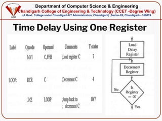
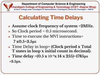
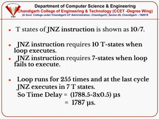
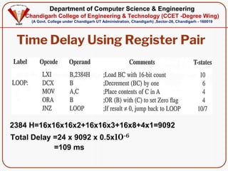
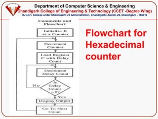
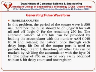
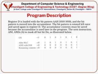
Department of Computer Sc. & Engineering
Chandigarh College of Engineering & Technology (CCET -Degree
Wing)
(A Govt. College under Chandigarh UT Administration, Chandigarh)
Sector-26, Chandigarh - 160019
MICROPROCESSOR
CS-304
DELAYS AND COUNTERS
Department of Computer Science & Engineering
Chandigarh College of Engineering & Technology (CCET -Degree Wing)
(A Govt. College under Chandigarh UT Administration, Chandigarh) ,Sector-26, Chandigarh - 160019
Topics We’ll Cover
• Counters and Time Delays
• Hexadecimal Counters
• Modulo Ten Counter
• Generating Pulse Waveform
• Debugging Counters and Time
Delay Programs
CS-604
Department of Computer Science & Engineering
Chandigarh College of Engineering & Technology (CCET -Degree Wing)
(A Govt. College under Chandigarh UT Administration, Chandigarh) ,Sector-26, Chandigarh - 160019
Introduction
⚫ This chapter deals with designing of counters and time
delays through software programming.
⚫ Counter and time delays are important technique. They
are commonly used in designing of traffic signals,
digital clocks, setting up reasonably accurate timing
between two events.
Department of Computer Science & Engineering
Chandigarh College of Engineering & Technology (CCET -Degree Wing)
(A Govt. College under Chandigarh UT Administration, Chandigarh) ,Sector-26, Chandigarh - 160019
Counters
⚫ Designing a counter: A counter is
determined by loading an appropriate
count in the register.
⚫ A loop is setup to decrement the count
(down-counter) and increment the count
for (up- counter) when an event occurs.
Department of Computer Science & Engineering
Chandigarh College of Engineering & Technology (CCET -Degree Wing)
(A Govt. College under Chandigarh UT Administration, Chandigarh) ,Sector-26, Chandigarh - 160019
Time -Delays
⚫ The procedure for designing a time delay is
same as counter.
⚫ A number is loaded in the register, depending
upon the delay required .
⚫ The register is decremented until count is not
equal to zero by setting a loop.
⚫ A conditional jump is executed when the count
is equal to zero.
⚫ The loop causes delay depending upon the
clock period of the system and number of
instructions.
Department of Computer Science & Engineering
Chandigarh College of Engineering & Technology (CCET -Degree Wing)
(A Govt. College under Chandigarh UT Administration, Chandigarh) ,Sector-26, Chandigarh - 160019
Time Delay Using One Register
Department of Computer Science & Engineering
Chandigarh College of Engineering & Technology (CCET -Degree Wing)
(A Govt. College under Chandigarh UT Administration, Chandigarh) ,Sector-26, Chandigarh - 160019
Calculating Time Delays
⚫ Assume clock frequency of system =2MHz.
⚫ So Clock period = 0.5 microsecond.
⚫ Time to execute the MVI instructions=
7 x0.5=3.5µs
⚫ Time Delay in loop= (Clock period x Total
T states in loop x initial count in decimal).
⚫ Time delay =(0.5 x 10-6x 14 x 255)=1785µs
+3.5µs.
Department of Computer Science & Engineering
Chandigarh College of Engineering & Technology (CCET -Degree Wing)
(A Govt. College under Chandigarh UT Administration, Chandigarh) ,Sector-26, Chandigarh - 160019
⚫ T states of JNZ instruction is shown as 10/7.
⚫ JNZ instruction requires 10 T-states when
loop executes.
⚫ JNZ instruction requires 7-states when loop
fails to execute.
⚫ Loop runs for 255 times and at the last cycle
JNZ executes in 7 T states.
So Time Delay = (1788.5-3x0.5) µs
= 1787 µs.
Department of Computer Science & Engineering
Chandigarh College of Engineering & Technology (CCET -Degree Wing)
(A Govt. College under Chandigarh UT Administration, Chandigarh) ,Sector-26, Chandigarh - 160019
Time Delay Using Register Pair
2384 H=16x16x16x2+16x16x3+16x8+4x1=9092
Total Delay =24 x 9092 x 0.5x10-6
=109 ms
Department of Computer Science & Engineering
Chandigarh College of Engineering & Technology (CCET -Degree Wing)
(A Govt. College under Chandigarh UT Administration, Chandigarh) ,Sector-26, Chandigarh - 160019
Flowchart for
Hexadecimal
counter
Department of Computer Science & Engineering
Chandigarh College of Engineering & Technology (CCET -Degree Wing)
(A Govt. College under Chandigarh UT Administration, Chandigarh) ,Sector-26, Chandigarh - 160019
Generating Pulse Waveform
⚫ PROBLEM ANALYSIS
In this problem, the period of the square wave is 500
us•, therefore, the pulse should be on (logic l) for 250
uS and off (logic 0) for the remaining 250 Its. The
alternate pattern of 0/l bits can be provided by
loading the accumulator with the number AAH (1010
1010) and rotating the pattern once through each
delay loop. Bit Do of the output port is used to
provide logic 0 and l; therefore, all other bits can be
masked by ANDing the accumulator with the byte 01
H. The delay of 250 us can be very easily obtained
with an 8-bit delay count and one register.
Department of Computer Science & Engineering
Chandigarh College of Engineering & Technology (CCET -Degree Wing)
(A Govt. College under Chandigarh UT Administration, Chandigarh) ,Sector-26, Chandigarh - 160019
Pro
gra
m
Department of Computer Science & Engineering
Chandigarh College of Engineering & Technology (CCET -Degree Wing)
(A Govt. College under Chandigarh UT Administration, Chandigarh) ,Sector-26, Chandigarh - 160019
Program Description
Register D is loaded with the bit pattern AAH (1010 1010), and the bit
pattern is moved into the accumulator. The bit pattern is rotated left once
and saved again in register D. The accumulator contents must be saved
because the accumulator is used later in the program. The next instruction,
ANI, ANDs (A) to mask all but bit Do, as illustrated below.
Department of Computer Science & Engineering
Chandigarh College of Engineering & Technology (CCET -Degree Wing)
(A Govt. College under Chandigarh UT Administration, Chandigarh) ,Sector-26, Chandigarh - 160019
⚫ Delay Calculations In this problem, the pulse
width is relatively small (250 us); therefore, to
obtain a reasonably accurate output pulse
width, we should account for all the T-states.
The total delay should include the delay in the
loop and the execution time of theinstructions
outside the loop.
Department of Computer Science & Engineering
Chandigarh College of Engineering & Technology (CCET -Degree Wing)
(A Govt. College under Chandigarh UT Administration, Chandigarh) ,Sector-26, Chandigarh - 160019
1. The number of instructions outside the loop is seven; it includes
six instructions before the loop beginning at the symbol ROTATE
and the last instruction JMP.
Delay outside the Loop: To = 46 T-states x 325 ns — 14.95 us
2. The delay loop includes two instructions (DCR and JNZ) with 14
T-states except for the last cycle, which has II T-states.
Loop Delay: TL = 14 T-states x 325 ns x (Count - l) + 11 T-states x
325 ns
= 4.5 us (Count- l) + 3.575
3. The total delay required is 250 ps. Therefore, the count can be
calculated as follows:
250us - 14.95us +4.5us (Count - 1) + 3.575us
Count =52.410 = 34H
Department of Computer Science & Engineering
Chandigarh College of Engineering & Technology (CCET -Degree Wing)
(A Govt. College under Chandigarh UT Administration, Chandigarh) ,Sector-26, Chandigarh - 160019
Debugging Counter & Time Delay Programs
⚫ Errors in counting T-states in a delay loop. Typically, the
first instruction—to load a delay register—is mistakenly
included in the loop.
⚫ Errors in recognizing how many times a loop is repeated.
⚫ Failure to convert a delay count from a decimal number
into its hexadecimal equivalent.
⚫ Conversion error in converting a delay count from
decimal to hexadecimal number or vice versa.
⚫ Specifying a wrong Jump location.
⚫ Failure to set a flag, especially with 16-bit
Decrement/lncrement instructions.
⚫ Using a wrong Jump instruction.
⚫ Failure to display either the first or the last count.
⚫ Failure to provide a delay between the last and the last-
but-one count.
Department of Computer Science & Engineering
Chandigarh College of Engineering & Technology (CCET -Degree Wing)
(A Govt. College under Chandigarh UT Administration, Chandigarh) ,Sector-26, Chandigarh - 160019
THANK YOU!
Any Queries?
CS-604

Delays and counter.pptx

  • 1.
    Department of ComputerSc. & Engineering Chandigarh College of Engineering & Technology (CCET -Degree Wing) (A Govt. College under Chandigarh UT Administration, Chandigarh) Sector-26, Chandigarh - 160019 MICROPROCESSOR CS-304 DELAYS AND COUNTERS
  • 2.
    Department of ComputerScience & Engineering Chandigarh College of Engineering & Technology (CCET -Degree Wing) (A Govt. College under Chandigarh UT Administration, Chandigarh) ,Sector-26, Chandigarh - 160019 Topics We’ll Cover • Counters and Time Delays • Hexadecimal Counters • Modulo Ten Counter • Generating Pulse Waveform • Debugging Counters and Time Delay Programs CS-604
  • 3.
    Department of ComputerScience & Engineering Chandigarh College of Engineering & Technology (CCET -Degree Wing) (A Govt. College under Chandigarh UT Administration, Chandigarh) ,Sector-26, Chandigarh - 160019 Introduction ⚫ This chapter deals with designing of counters and time delays through software programming. ⚫ Counter and time delays are important technique. They are commonly used in designing of traffic signals, digital clocks, setting up reasonably accurate timing between two events.
  • 4.
    Department of ComputerScience & Engineering Chandigarh College of Engineering & Technology (CCET -Degree Wing) (A Govt. College under Chandigarh UT Administration, Chandigarh) ,Sector-26, Chandigarh - 160019 Counters ⚫ Designing a counter: A counter is determined by loading an appropriate count in the register. ⚫ A loop is setup to decrement the count (down-counter) and increment the count for (up- counter) when an event occurs.
  • 5.
    Department of ComputerScience & Engineering Chandigarh College of Engineering & Technology (CCET -Degree Wing) (A Govt. College under Chandigarh UT Administration, Chandigarh) ,Sector-26, Chandigarh - 160019 Time -Delays ⚫ The procedure for designing a time delay is same as counter. ⚫ A number is loaded in the register, depending upon the delay required . ⚫ The register is decremented until count is not equal to zero by setting a loop. ⚫ A conditional jump is executed when the count is equal to zero. ⚫ The loop causes delay depending upon the clock period of the system and number of instructions.
  • 6.
    Department of ComputerScience & Engineering Chandigarh College of Engineering & Technology (CCET -Degree Wing) (A Govt. College under Chandigarh UT Administration, Chandigarh) ,Sector-26, Chandigarh - 160019 Time Delay Using One Register
  • 7.
    Department of ComputerScience & Engineering Chandigarh College of Engineering & Technology (CCET -Degree Wing) (A Govt. College under Chandigarh UT Administration, Chandigarh) ,Sector-26, Chandigarh - 160019 Calculating Time Delays ⚫ Assume clock frequency of system =2MHz. ⚫ So Clock period = 0.5 microsecond. ⚫ Time to execute the MVI instructions= 7 x0.5=3.5µs ⚫ Time Delay in loop= (Clock period x Total T states in loop x initial count in decimal). ⚫ Time delay =(0.5 x 10-6x 14 x 255)=1785µs +3.5µs.
  • 8.
    Department of ComputerScience & Engineering Chandigarh College of Engineering & Technology (CCET -Degree Wing) (A Govt. College under Chandigarh UT Administration, Chandigarh) ,Sector-26, Chandigarh - 160019 ⚫ T states of JNZ instruction is shown as 10/7. ⚫ JNZ instruction requires 10 T-states when loop executes. ⚫ JNZ instruction requires 7-states when loop fails to execute. ⚫ Loop runs for 255 times and at the last cycle JNZ executes in 7 T states. So Time Delay = (1788.5-3x0.5) µs = 1787 µs.
  • 9.
    Department of ComputerScience & Engineering Chandigarh College of Engineering & Technology (CCET -Degree Wing) (A Govt. College under Chandigarh UT Administration, Chandigarh) ,Sector-26, Chandigarh - 160019 Time Delay Using Register Pair 2384 H=16x16x16x2+16x16x3+16x8+4x1=9092 Total Delay =24 x 9092 x 0.5x10-6 =109 ms
  • 10.
    Department of ComputerScience & Engineering Chandigarh College of Engineering & Technology (CCET -Degree Wing) (A Govt. College under Chandigarh UT Administration, Chandigarh) ,Sector-26, Chandigarh - 160019 Flowchart for Hexadecimal counter
  • 11.
    Department of ComputerScience & Engineering Chandigarh College of Engineering & Technology (CCET -Degree Wing) (A Govt. College under Chandigarh UT Administration, Chandigarh) ,Sector-26, Chandigarh - 160019 Generating Pulse Waveform ⚫ PROBLEM ANALYSIS In this problem, the period of the square wave is 500 us•, therefore, the pulse should be on (logic l) for 250 uS and off (logic 0) for the remaining 250 Its. The alternate pattern of 0/l bits can be provided by loading the accumulator with the number AAH (1010 1010) and rotating the pattern once through each delay loop. Bit Do of the output port is used to provide logic 0 and l; therefore, all other bits can be masked by ANDing the accumulator with the byte 01 H. The delay of 250 us can be very easily obtained with an 8-bit delay count and one register.
  • 12.
    Department of ComputerScience & Engineering Chandigarh College of Engineering & Technology (CCET -Degree Wing) (A Govt. College under Chandigarh UT Administration, Chandigarh) ,Sector-26, Chandigarh - 160019 Pro gra m
  • 13.
    Department of ComputerScience & Engineering Chandigarh College of Engineering & Technology (CCET -Degree Wing) (A Govt. College under Chandigarh UT Administration, Chandigarh) ,Sector-26, Chandigarh - 160019 Program Description Register D is loaded with the bit pattern AAH (1010 1010), and the bit pattern is moved into the accumulator. The bit pattern is rotated left once and saved again in register D. The accumulator contents must be saved because the accumulator is used later in the program. The next instruction, ANI, ANDs (A) to mask all but bit Do, as illustrated below.
  • 14.
    Department of ComputerScience & Engineering Chandigarh College of Engineering & Technology (CCET -Degree Wing) (A Govt. College under Chandigarh UT Administration, Chandigarh) ,Sector-26, Chandigarh - 160019 ⚫ Delay Calculations In this problem, the pulse width is relatively small (250 us); therefore, to obtain a reasonably accurate output pulse width, we should account for all the T-states. The total delay should include the delay in the loop and the execution time of theinstructions outside the loop.
  • 15.
    Department of ComputerScience & Engineering Chandigarh College of Engineering & Technology (CCET -Degree Wing) (A Govt. College under Chandigarh UT Administration, Chandigarh) ,Sector-26, Chandigarh - 160019 1. The number of instructions outside the loop is seven; it includes six instructions before the loop beginning at the symbol ROTATE and the last instruction JMP. Delay outside the Loop: To = 46 T-states x 325 ns — 14.95 us 2. The delay loop includes two instructions (DCR and JNZ) with 14 T-states except for the last cycle, which has II T-states. Loop Delay: TL = 14 T-states x 325 ns x (Count - l) + 11 T-states x 325 ns = 4.5 us (Count- l) + 3.575 3. The total delay required is 250 ps. Therefore, the count can be calculated as follows: 250us - 14.95us +4.5us (Count - 1) + 3.575us Count =52.410 = 34H
  • 16.
    Department of ComputerScience & Engineering Chandigarh College of Engineering & Technology (CCET -Degree Wing) (A Govt. College under Chandigarh UT Administration, Chandigarh) ,Sector-26, Chandigarh - 160019 Debugging Counter & Time Delay Programs ⚫ Errors in counting T-states in a delay loop. Typically, the first instruction—to load a delay register—is mistakenly included in the loop. ⚫ Errors in recognizing how many times a loop is repeated. ⚫ Failure to convert a delay count from a decimal number into its hexadecimal equivalent. ⚫ Conversion error in converting a delay count from decimal to hexadecimal number or vice versa. ⚫ Specifying a wrong Jump location. ⚫ Failure to set a flag, especially with 16-bit Decrement/lncrement instructions. ⚫ Using a wrong Jump instruction. ⚫ Failure to display either the first or the last count. ⚫ Failure to provide a delay between the last and the last- but-one count.
  • 17.
    Department of ComputerScience & Engineering Chandigarh College of Engineering & Technology (CCET -Degree Wing) (A Govt. College under Chandigarh UT Administration, Chandigarh) ,Sector-26, Chandigarh - 160019 THANK YOU! Any Queries? CS-604