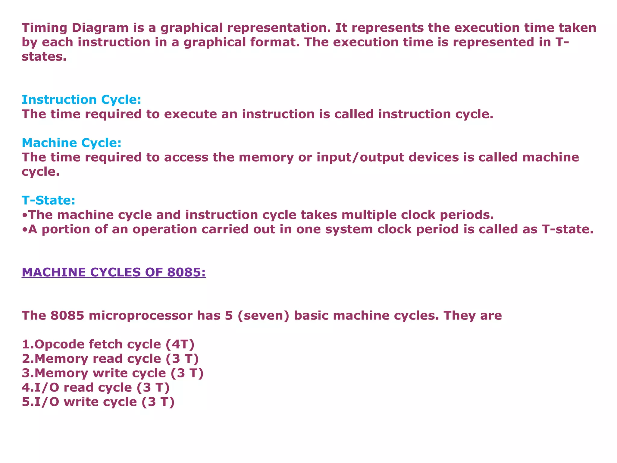
Timing Diagram is a graphical representation. It represents the execution time taken
by each instruction in a graphical format. The execution time is represented in T-
states.


Instruction Cycle:
The time required to execute an instruction is called instruction cycle.

Machine Cycle:
The time required to access the memory or input/output devices is called machine
cycle.

T-State:
•The machine cycle and instruction cycle takes multiple clock periods.
•A portion of an operation carried out in one system clock period is called as T-state.


MACHINE CYCLES OF 8085:


The 8085 microprocessor has 5 (seven) basic machine cycles. They are

1.Opcode fetch cycle (4T)
2.Memory read cycle (3 T)
3.Memory write cycle (3 T)
4.I/O read cycle (3 T)
5.I/O write cycle (3 T)
Timing diagram for MVI B, 43H.


Fetching the Opcode 06H from the memory 2000H. (OF machine cycle)


Read (move) the data 43H from memory 2001H. (memory read)
MVI B, data
  
Timing diagram for INR M (INR 4250)
 
 Fetching the Opcode 34H from the memory 4105H. (OF cycle)


 Let the memory address (M) be 4250H. (MR cycle -To read Memory address
and data)


 Let the content of that memory is 12H.


 Increment the memory content from 12H to 13H. (MW CYCLE)
INR M
ADD M
Timing diagram for STA 526AH:
 
STA means Store Accumulator -The contents of the accumulator is stored in the specified
address (526A).


The opcode of the STA instruction is said to be 32H. It is fetched from the memory 41FFH
(OF machine cycle)


Then the lower order memory address is read(6A). - Memory Read Machine Cycle


Read the higher order memory address (52).- Memory Read Machine Cycle


The combination of both the addresses are considered and the content from accumulatoris
written in 526A. - Memory Write Machine Cycle


Assume the memory address for the instruction and let the content of accumulator isC7H. So
C7H from accumulator is now stored in 526A
STA addr
IN Byte
Copy H and L registers to the stack pointer
SPHL       none The instruction loads the contents of the H and L registers
into the stack pointer register, the contents of the H register provide
the high-order address and the contents of the L register provide the
low-order address. The contents of the H and L registers are not altered.
  Example: SPHL

Exchange H and L with top of stack
XTHL       none The contents of the L register are exchanged with the
stack location pointed out by the contents of the stack pointer
register. The contents of the H register are exchanged with the next stack
location (SP+1); however, the contents of the stack pointer register are not
altered.
  Example: XTHL
Push register pair onto stack
PUSH        Reg. pair The contents of the register pair designated in the
operand are copied onto the stack in the following sequence. The stack
pointer register is decremented and the contents of the high-order register
(B, D, H, A) are copied into that location. The stack pointer register is
decremented again and the contents of the low-order register (C, E, L,
flags) are copied to that location.
 Example: PUSH B or PUSH A
Pop off stack to register pair
POP        Reg. pair      The contents of the memory location pointed out by the
stack
                           pointer register are copied to the low-order register (C, E, L,
                           status flags) of the operand. The stack pointer incremented
                           by 1 and the contents of that memory location are copied to
                           the high-order register (B, D, H, A) of the operand. The
                           stack pointer register is again incremented by 1.
Example: POP H or POP A

No operation
NOP       none           No operation is performed. The instruction is fetched and
                         decoded. However no operation is executed.
Example: NOP

Halt and enter wait state
HLT       none            The CPU finishes executing the current instruction and halts
                          any further execution. An interrupt or reset is necessary
                          to exit from the halt state.
Example: HLT
LDA C020H
MOV E,A
MVI D,00H
LDA C021H
MOV C,A
LXI H,0000H
BACK:
DAD D
DCR C
JNZ BACK
SHLD C030H
HLT

T imingdiagram

  • 1.
    Timing Diagram isa graphical representation. It represents the execution time taken by each instruction in a graphical format. The execution time is represented in T- states. Instruction Cycle: The time required to execute an instruction is called instruction cycle. Machine Cycle: The time required to access the memory or input/output devices is called machine cycle. T-State: •The machine cycle and instruction cycle takes multiple clock periods. •A portion of an operation carried out in one system clock period is called as T-state. MACHINE CYCLES OF 8085: The 8085 microprocessor has 5 (seven) basic machine cycles. They are 1.Opcode fetch cycle (4T) 2.Memory read cycle (3 T) 3.Memory write cycle (3 T) 4.I/O read cycle (3 T) 5.I/O write cycle (3 T)
  • 4.
    Timing diagram forMVI B, 43H. Fetching the Opcode 06H from the memory 2000H. (OF machine cycle) Read (move) the data 43H from memory 2001H. (memory read)
  • 5.
  • 6.
       Timing diagram forINR M (INR 4250)    Fetching the Opcode 34H from the memory 4105H. (OF cycle)  Let the memory address (M) be 4250H. (MR cycle -To read Memory address and data)  Let the content of that memory is 12H.  Increment the memory content from 12H to 13H. (MW CYCLE)
  • 7.
  • 8.
  • 9.
    Timing diagram forSTA 526AH:   STA means Store Accumulator -The contents of the accumulator is stored in the specified address (526A). The opcode of the STA instruction is said to be 32H. It is fetched from the memory 41FFH (OF machine cycle) Then the lower order memory address is read(6A). - Memory Read Machine Cycle Read the higher order memory address (52).- Memory Read Machine Cycle The combination of both the addresses are considered and the content from accumulatoris written in 526A. - Memory Write Machine Cycle Assume the memory address for the instruction and let the content of accumulator isC7H. So C7H from accumulator is now stored in 526A
  • 10.
  • 11.
  • 13.
    Copy H andL registers to the stack pointer SPHL none The instruction loads the contents of the H and L registers into the stack pointer register, the contents of the H register provide the high-order address and the contents of the L register provide the low-order address. The contents of the H and L registers are not altered. Example: SPHL Exchange H and L with top of stack XTHL none The contents of the L register are exchanged with the stack location pointed out by the contents of the stack pointer register. The contents of the H register are exchanged with the next stack location (SP+1); however, the contents of the stack pointer register are not altered. Example: XTHL Push register pair onto stack PUSH Reg. pair The contents of the register pair designated in the operand are copied onto the stack in the following sequence. The stack pointer register is decremented and the contents of the high-order register (B, D, H, A) are copied into that location. The stack pointer register is decremented again and the contents of the low-order register (C, E, L, flags) are copied to that location. Example: PUSH B or PUSH A
  • 14.
    Pop off stackto register pair POP Reg. pair The contents of the memory location pointed out by the stack pointer register are copied to the low-order register (C, E, L, status flags) of the operand. The stack pointer incremented by 1 and the contents of that memory location are copied to the high-order register (B, D, H, A) of the operand. The stack pointer register is again incremented by 1. Example: POP H or POP A No operation NOP none No operation is performed. The instruction is fetched and decoded. However no operation is executed. Example: NOP Halt and enter wait state HLT none The CPU finishes executing the current instruction and halts any further execution. An interrupt or reset is necessary to exit from the halt state. Example: HLT
  • 15.
    LDA C020H MOV E,A MVID,00H LDA C021H MOV C,A LXI H,0000H BACK: DAD D DCR C JNZ BACK SHLD C030H HLT