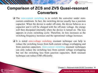
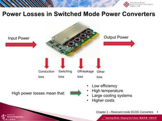
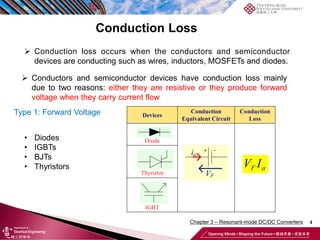
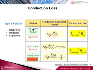
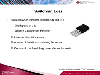
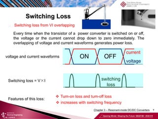
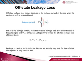
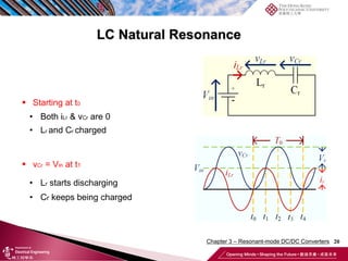
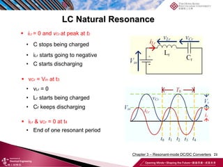
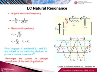
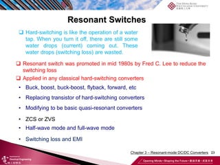
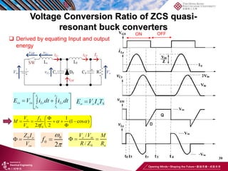
This chapter discusses resonant DC/DC converters. Hard-switching converters experience high switching losses which reduce efficiency. Resonant converters reduce switching losses by forcing zero-current or zero-voltage switching through resonant circuits. This is accomplished by adding inductors and capacitors to shape current and voltage waveforms. While more efficient, resonant converters have more complex circuitry than hard-switching converters.

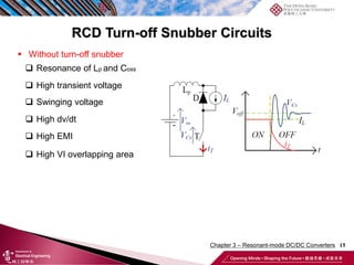
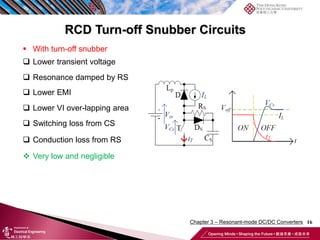


![30
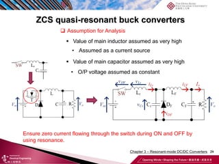
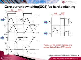
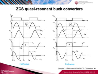
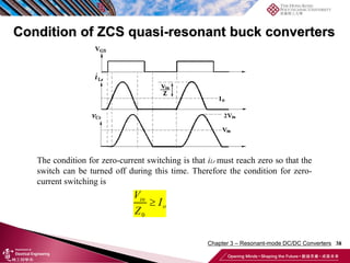
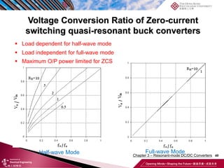
ZCS quasi-resonant buck converters
State I (Linear) [t0 – t1] State II (Resonant) [t1 – t2]
State III (Recovering) [t2 – t3] State IV (Free Wheeling) [t3 – t4]
Chapter 3 – Resonant-mode DC/DC Converters](https://image.slidesharecdn.com/chapter3-resonant-modedc-dcconverter-221030084001-6a87bddc/85/Chapter-3-Resonant-mode-DC-DC-Converter-pdf-30-320.jpg)
![31
ZCS quasi-resonant buck converters
Duration of State I:
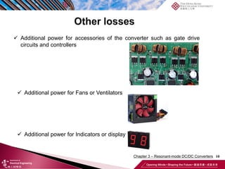
Boundary Condition at t1
State I (Linear) [t0 – t1] ON OFF
When switch is turned on at t0, diode
DF is still conducting the load current
Io through LF in the previous stage.](https://image.slidesharecdn.com/chapter3-resonant-modedc-dcconverter-221030084001-6a87bddc/85/Chapter-3-Resonant-mode-DC-DC-Converter-pdf-31-320.jpg)
![32
ZCS quasi-resonant buck converters
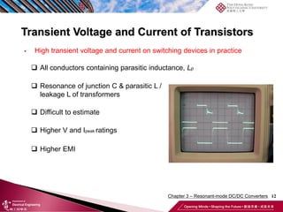
Angular Resonant Frequency
Resonant Impedance
State II (Resonant) [t1 – t2] ON OFF
Diode DF stops conducting.
Lr and Cr starts to
resonant.](https://image.slidesharecdn.com/chapter3-resonant-modedc-dcconverter-221030084001-6a87bddc/85/Chapter-3-Resonant-mode-DC-DC-Converter-pdf-32-320.jpg)
![33
ZCS quasi-resonant buck converters
State II (Resonant) [t1 – t2]
Boundary Condition at t2
Half-wave
Full-wave
at t2
ON OFF
0 2 1
( )
set t t
Switch can be
turned off after t2](https://image.slidesharecdn.com/chapter3-resonant-modedc-dcconverter-221030084001-6a87bddc/85/Chapter-3-Resonant-mode-DC-DC-Converter-pdf-33-320.jpg)
![34
ZCS quasi-resonant buck converters
Boundary Condition at t3
State III (Recovering) [t2 – t3]
Duration of State III
ON OFF
Resonant stops. Cr begins to be
discharged through LF with a
discharging current equal to Io](https://image.slidesharecdn.com/chapter3-resonant-modedc-dcconverter-221030084001-6a87bddc/85/Chapter-3-Resonant-mode-DC-DC-Converter-pdf-34-320.jpg)
![35
ZCS quasi-resonant buck converters
Duration of State IV
State IV (Free Wheeling) [t3 – t4] ON OFF
DF is conducting, output current
freewheels through DF.](https://image.slidesharecdn.com/chapter3-resonant-modedc-dcconverter-221030084001-6a87bddc/85/Chapter-3-Resonant-mode-DC-DC-Converter-pdf-35-320.jpg)
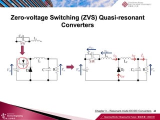
![ZVS Quasi-resonant Converters
43
State I (Linear) [t0 – t1] State II (Resonant) [t1 – t2]
State III (Recovering) [t2 – t3] State IV (Free Wheeling) [t3 – t4]
Chapter 3 – Resonant-mode DC/DC Converters](https://image.slidesharecdn.com/chapter3-resonant-modedc-dcconverter-221030084001-6a87bddc/85/Chapter-3-Resonant-mode-DC-DC-Converter-pdf-43-320.jpg)
![ZVS Quasi-resonant Converters
44
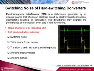
Duration of State I:
Boundary Condition at t1
State I (Linear) [t0 – t1] ON
OFF
Cr begins to be charged](https://image.slidesharecdn.com/chapter3-resonant-modedc-dcconverter-221030084001-6a87bddc/85/Chapter-3-Resonant-mode-DC-DC-Converter-pdf-44-320.jpg)
![ZVS Quasi-resonant Converters
45
Angular Resonant Frequency
Resonant Impedance
State II (Resonant) [t1 – t2] ON
OFF
When Cr increases to Vin, voltage
across DF becomes positive
Chapter 3 – Resonant-mode DC/DC Converters](https://image.slidesharecdn.com/chapter3-resonant-modedc-dcconverter-221030084001-6a87bddc/85/Chapter-3-Resonant-mode-DC-DC-Converter-pdf-45-320.jpg)
![ZVS Quasi-resonant Converters
46
State II (Resonant) [t1 – t2] ON
OFF
Boundary condition at t2
Half-wave
Full-wave
Chapter 3 – Resonant-mode DC/DC Converters](https://image.slidesharecdn.com/chapter3-resonant-modedc-dcconverter-221030084001-6a87bddc/85/Chapter-3-Resonant-mode-DC-DC-Converter-pdf-46-320.jpg)
![ZVS Quasi-resonant Converters
47
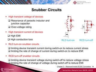
Boundary Condition at t3
Duration of State III:
State III (Recovering) [t2 – t3] ON
OFF
Resonance stops, Lr begins to be charged
by Vin. This state finishes when iLr reaches
Io, then DF on longer conducts
Switch can be
turned on after t2
Chapter 3 – Resonant-mode DC/DC Converters](https://image.slidesharecdn.com/chapter3-resonant-modedc-dcconverter-221030084001-6a87bddc/85/Chapter-3-Resonant-mode-DC-DC-Converter-pdf-47-320.jpg)
![ZVS Quasi-resonant Converters
48
State IV (Free Wheeling) [t3 – t4] ON
OFF
Output current Io freewheels through Lr and
switch SW.
Chapter 3 – Resonant-mode DC/DC Converters](https://image.slidesharecdn.com/chapter3-resonant-modedc-dcconverter-221030084001-6a87bddc/85/Chapter-3-Resonant-mode-DC-DC-Converter-pdf-48-320.jpg)