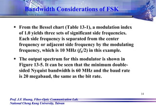
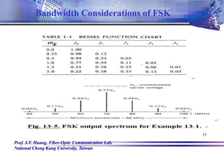
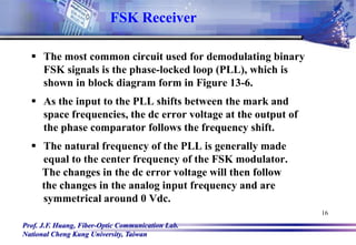
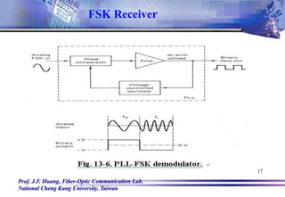
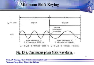
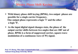
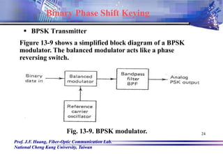
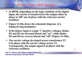
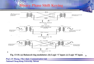
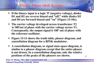
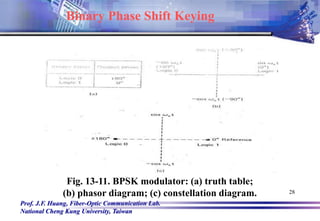
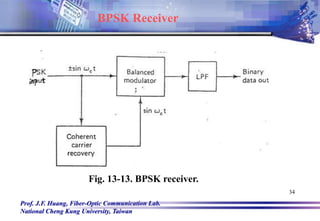
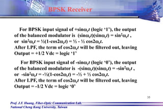
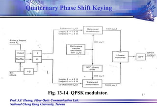
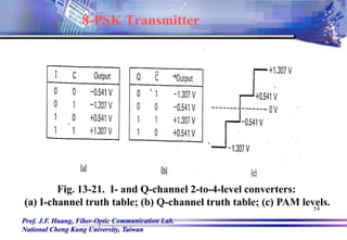
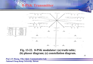
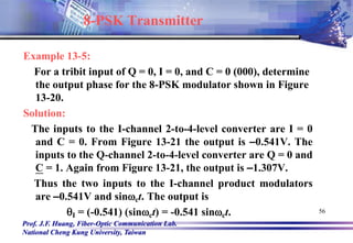
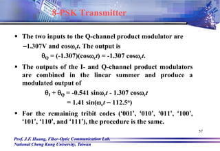
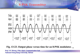
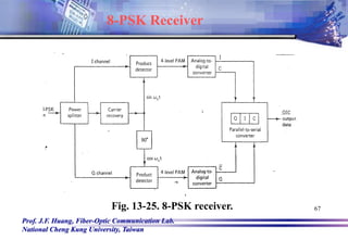
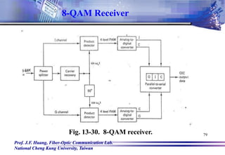
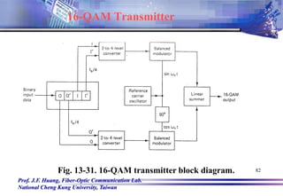
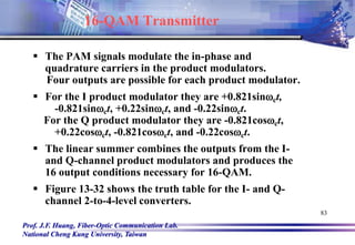
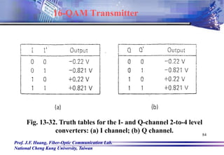
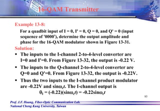
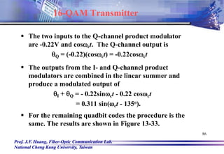
This document discusses various digital modulation techniques including Amplitude Shift Keying (ASK), Frequency Shift Keying (FSK), Phase Shift Keying (PSK), and their implementation. It provides mathematical expressions and diagrams to explain how each technique works. For ASK, a digital 1 or 0 is represented by the presence or absence of a carrier signal. For FSK, the frequency of the carrier shifts between mark and space frequencies. For BPSK, a digital 1 or 0 is represented by two phases of a carrier that are 180 degrees out of phase. Bandwidth requirements and receiver designs are also covered for each technique.

![Prof. J.F. Huang, Fiber-Optic Communication Lab.
National Cheng Kung University, Taiwan
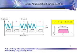
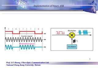
Amplitude Shift Keying (ASK)
Mathematically, ASK is
vask(t) = [1 vm(t)][A/2 cos(c t)]
For logic 1 , vm(t)=+1V
vask(t) = [1 1][A/2 cos(c t)] = Acos(c t)
For logic 0 , vm(t)=-1V
vask(t) = [1 - 1][A/2 cos(c t)] = 0
2](https://image.slidesharecdn.com/chap13-digitalmodulationtechniques-220919150610-6f624c77/85/Chap13-Digital-Modulation-Techniques-ppt-2-320.jpg)
![Prof. J.F. Huang, Fiber-Optic Communication Lab.
National Cheng Kung University, Taiwan
6
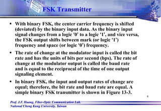
The general expression for a binary FSK signal is
v(t) = Vccos{2π[fc vm(t)Df)]t} (13-3)
where
v(t)= binary FSK waveform
Vc = peak unmodulated carrier amplitude
fc = carrier frequency
vm(t) = binary input modulating signal (volts)
Df = difference in output frequency
Frequency Shift Keying](https://image.slidesharecdn.com/chap13-digitalmodulationtechniques-220919150610-6f624c77/85/Chap13-Digital-Modulation-Techniques-ppt-6-320.jpg)
![Prof. J.F. Huang, Fiber-Optic Communication Lab.
National Cheng Kung University, Taiwan
64
Solution:
The bit rate in the I, Q, and C channels is equal to
one-third of the input bit rate, or
fbC=fbQ=fbI = 10Mbps/3 =3.33Mbps.
The faster rate of change and highest fundamental
frequency presented to either balanced modulator is
fa = fbC/2 = fbQ/2 = fbI/2
= 3.33Mbps/2 = 1.667Mbps
The output wave from the balance modulator is
(sin2fat)(sin2fct)
= ½[cos2(68.333MHz)t – cos2(71.667MHz)t]
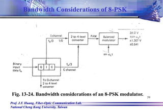
Bandwidth Considerations of 8-PSK](https://image.slidesharecdn.com/chap13-digitalmodulationtechniques-220919150610-6f624c77/85/Chap13-Digital-Modulation-Techniques-ppt-64-320.jpg)
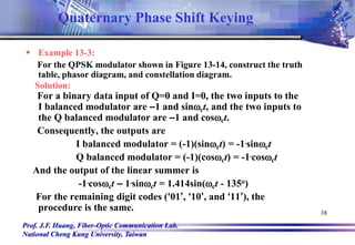
![Prof. J.F. Huang, Fiber-Optic Communication Lab.
National Cheng Kung University, Taiwan
94
Solution:
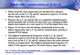
The bit rate in the I, I’, Q, and Q’ channels is equal to
1/4 of the input bit rate or
fbI = fbI’ = fbQ = fbQ’ = fb/4 = 10Mbps/4 = 2.5 Mbps
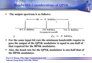
Therefore, the faster rate of change and highest
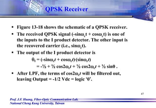
fundamental frequency presented to either balanced
modulator is
fa = fbI/2 = fbI’/2 = fbQ/2 = fbQ’/2
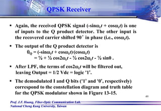
= 2.5 Mbps/2 = 1.25 Mbps
The output wave from the balanced modulator is
(sin2fat)(sin2fct)
= ½ cos[2(68.75MHz)t] - ½ cos[2(71.25MHz)t]
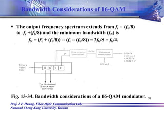
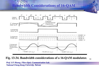
Bandwidth Considerations of 16-QAM](https://image.slidesharecdn.com/chap13-digitalmodulationtechniques-220919150610-6f624c77/85/Chap13-Digital-Modulation-Techniques-ppt-94-320.jpg)
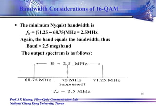
![Prof. J.F. Huang, Fiber-Optic Communication Lab.
National Cheng Kung University, Taiwan
101
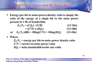
Carrier power can be stated in watts or dBm, where
C(dBm) = 10log[C(watts)/0.001] (13-13)
Thermal noise power is expressed mathematically as
N = kTB (watts) (13-14a)
or N(dBm) = 10log(kTB/0.001) (13-14b)
Mathematically, the carrier-to-noise power ratio is
C/N = C/kTB (13-15a)
where
C = Carrier power (W)
N = thermal noise power (W)
k = Boltzmann's constant (1.38×10⁻²³ J/oK)
T = temperature (0oK = -273 oC, Room temp. = 290oK)
B = bandwidth (Hz).
Probability of Error and Bit Error Rate](https://image.slidesharecdn.com/chap13-digitalmodulationtechniques-220919150610-6f624c77/85/Chap13-Digital-Modulation-Techniques-ppt-101-320.jpg)