Download as PDF, PPTX
![Si = Ai ⊕ Bi ⊕Ci-1= Pi ⊕ Ci-1 [Pi = Ai ⊕ Bi ]
Ci = AiBi + (Ai ⊕ Bi )Ci-1 = Gi + PiCi-1 [Gi = AiBi ]
Time delay = 3τ = (2n +1)](https://image.slidesharecdn.com/carrylookaheadadder-240725064751-7b9cb0d6/75/Carry-Look-Ahead-Adder-ALU-Encoders-and-Decoders-2-2048.jpg)
![Carry look ahead adder
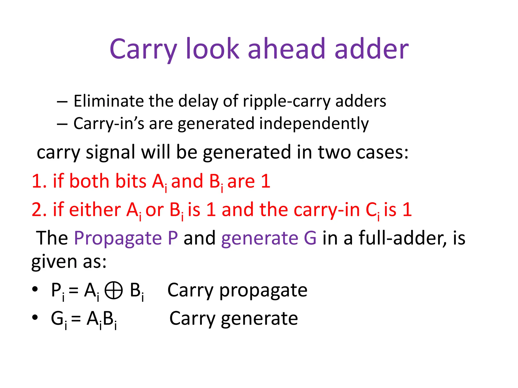
• The new expressions for the output sum and the carryout
are given by:
• Si = Ai ⊕ Bi ⊕Ci-1= Pi ⊕ Ci-1 [Pi = Ai ⊕ Bi ]
• Ci = AiBi + (Ai ⊕ Bi )Ci-1 = Gi + PiCi-1 [Gi = AiBi ]
Let's apply these equations for a 4-bit adder
• C0 = G0 + P0C-1
• C1 = G1 + P1C0 = G1 + P1(G0 + P0C-1) = G1 + P1G0 + P1P0C-1
• C2 = G2 + P2C1 = G2 + P2G1 + P2 P1G0 + P2P1P0C-1
• C3 = G3 + P3C2 = G3 + P3G2 +P3P2G1 +P3P2 P1G0 +
P3P2P1P0C-1
These expressions show that C1, C2 and C3 do not depend on
its previous carry-in](https://image.slidesharecdn.com/carrylookaheadadder-240725064751-7b9cb0d6/75/Carry-Look-Ahead-Adder-ALU-Encoders-and-Decoders-4-2048.jpg)
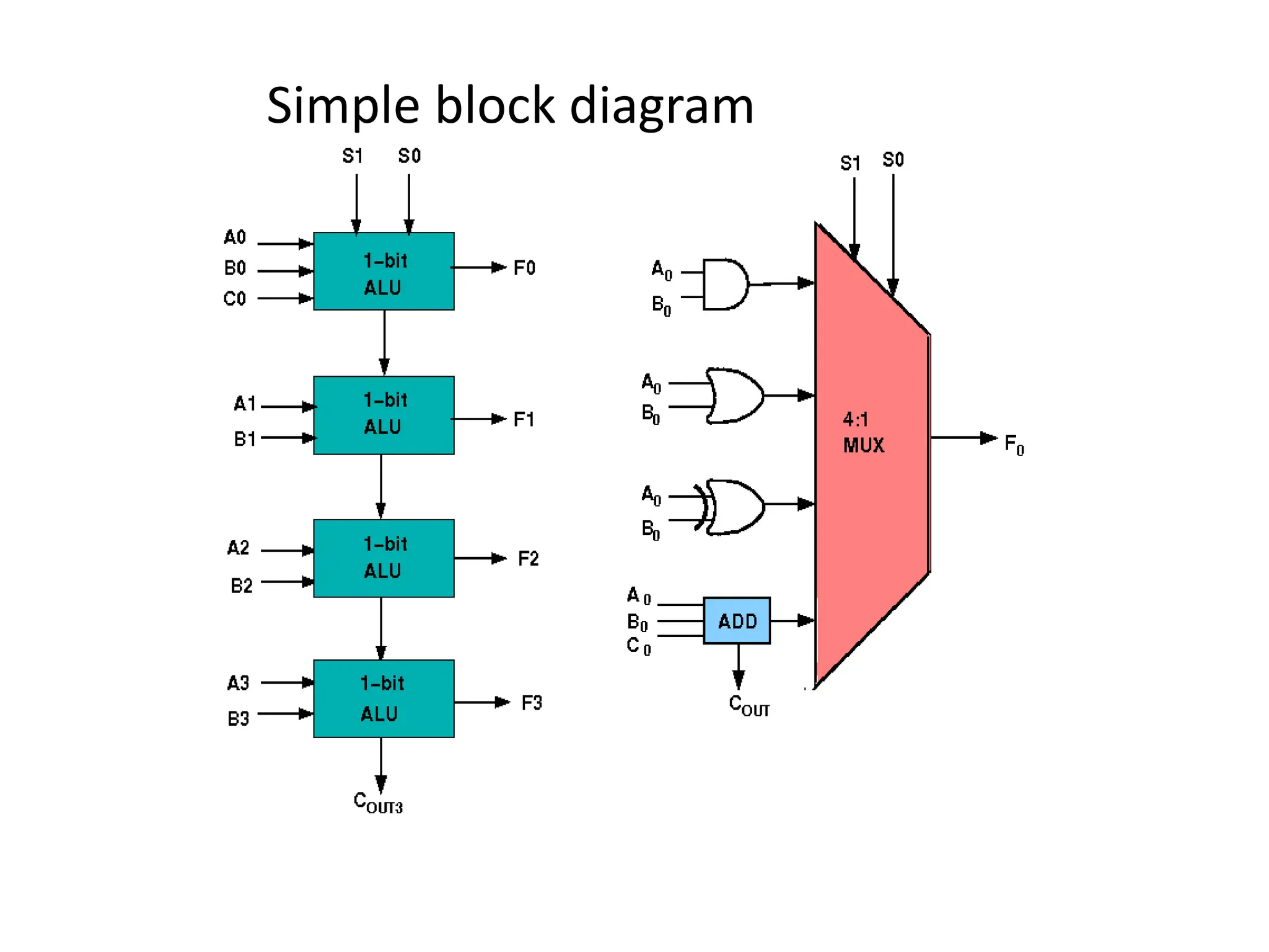
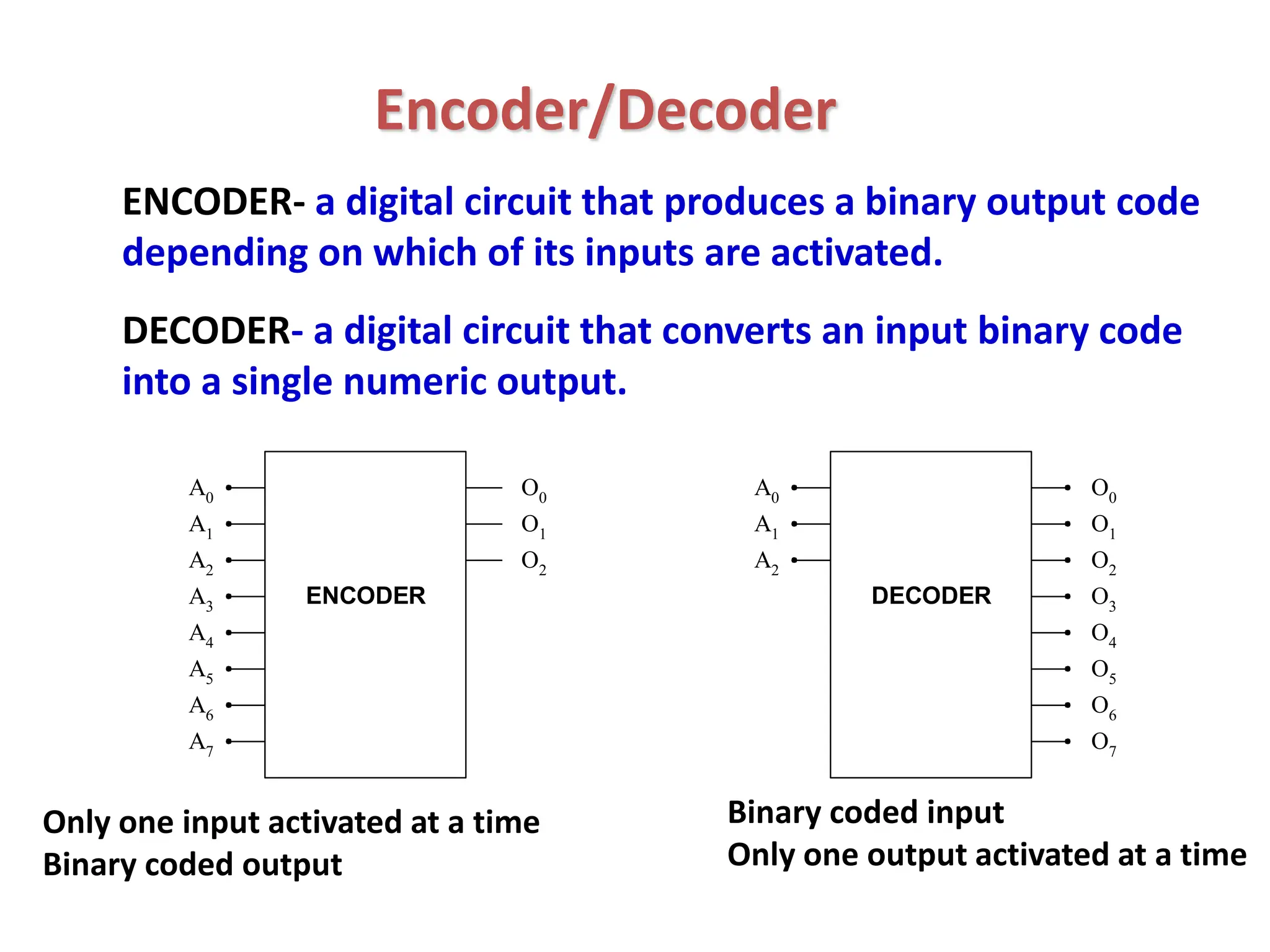
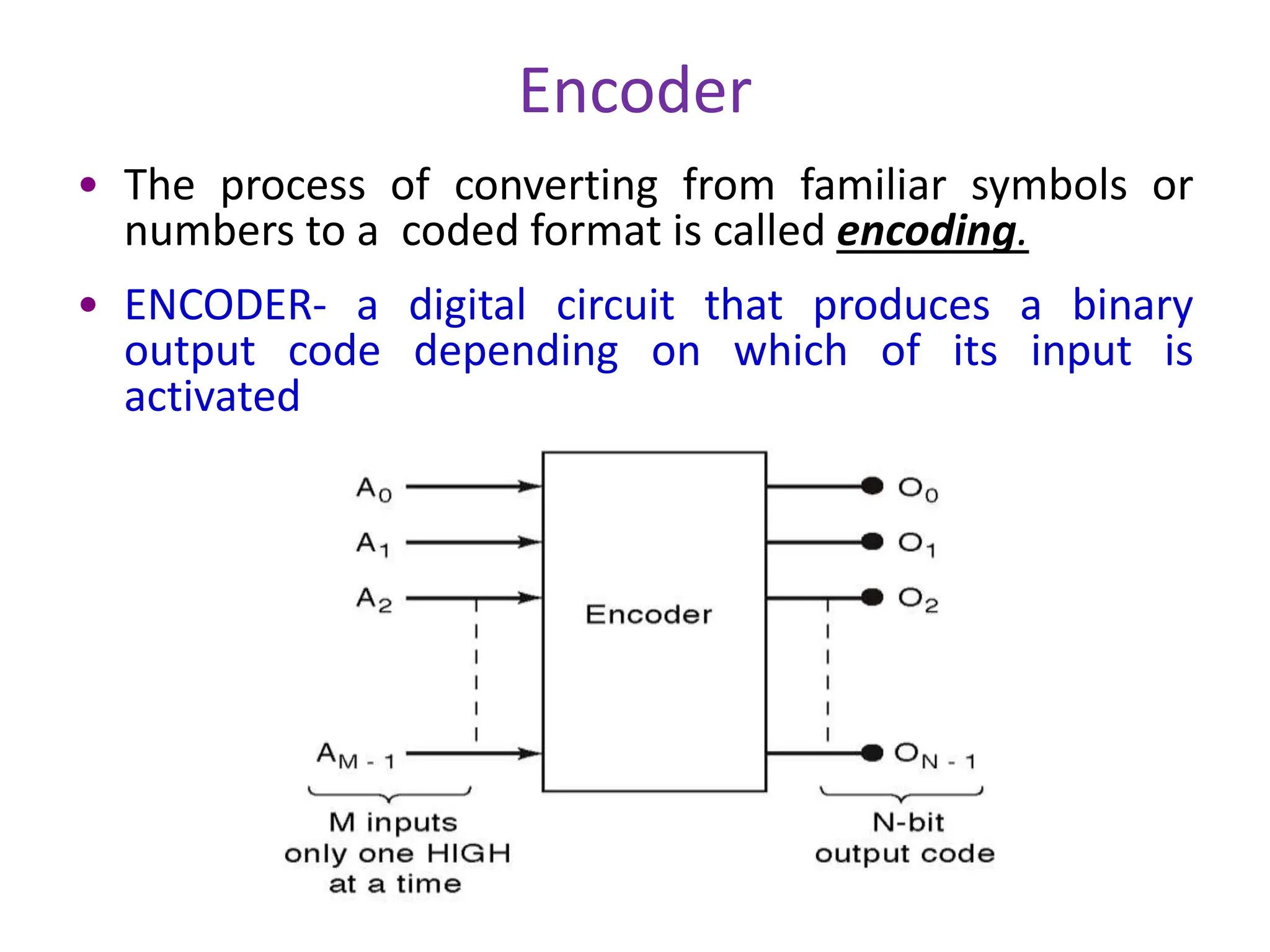
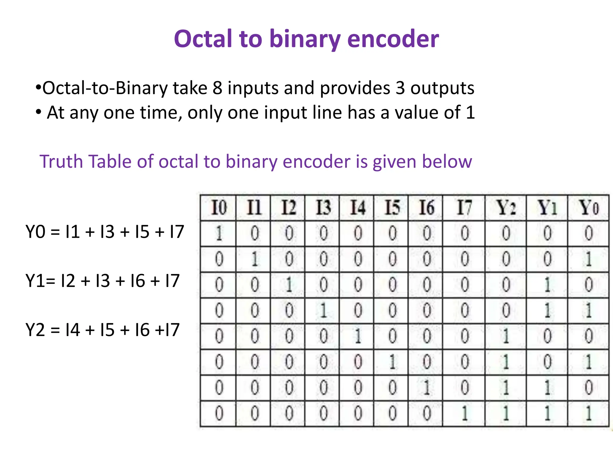
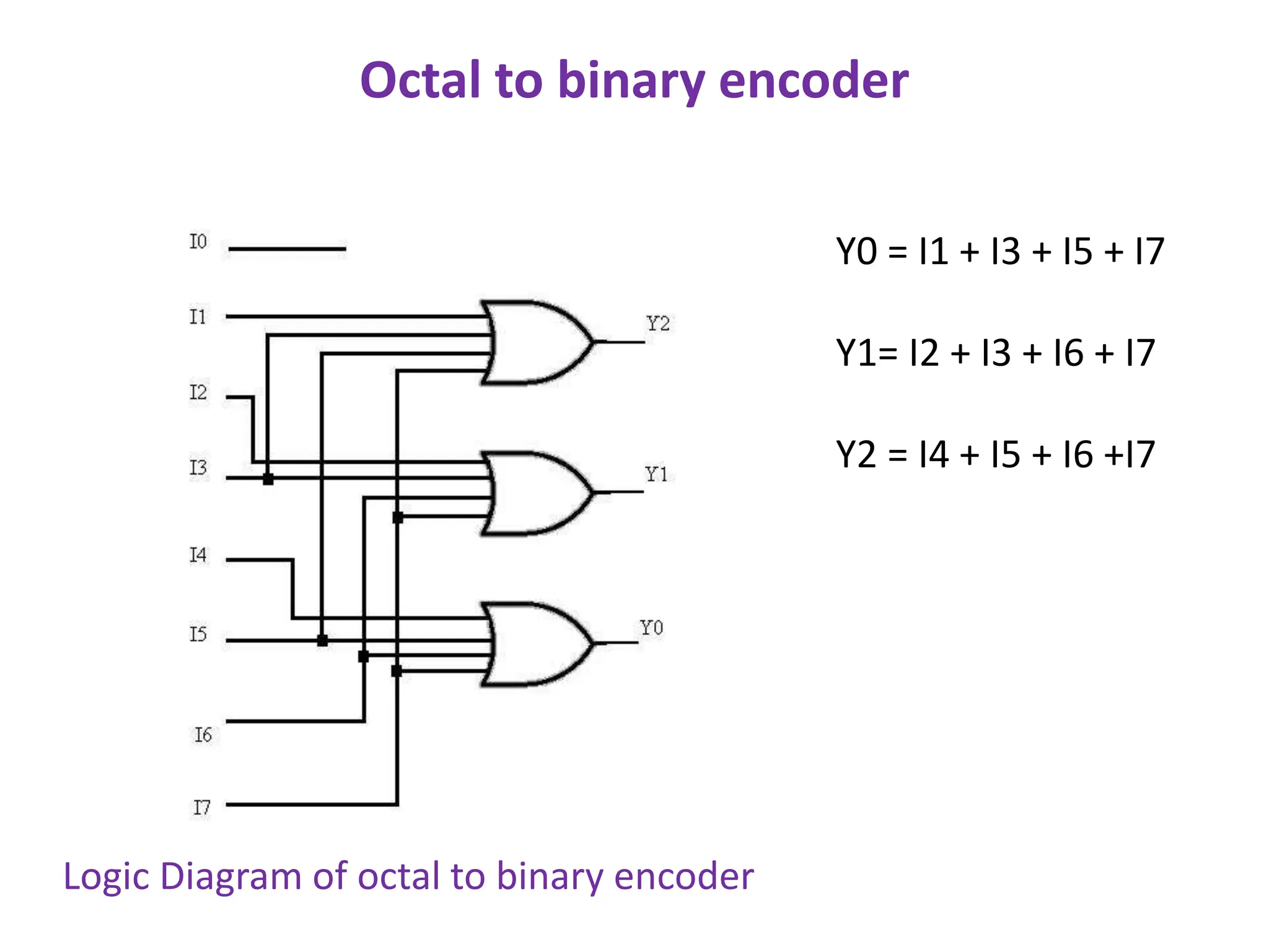
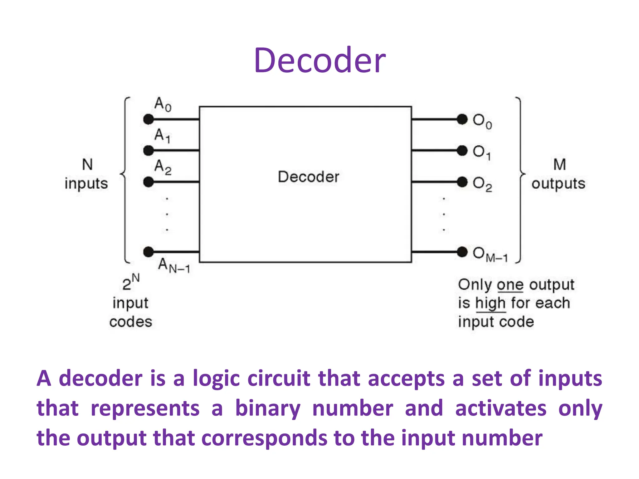
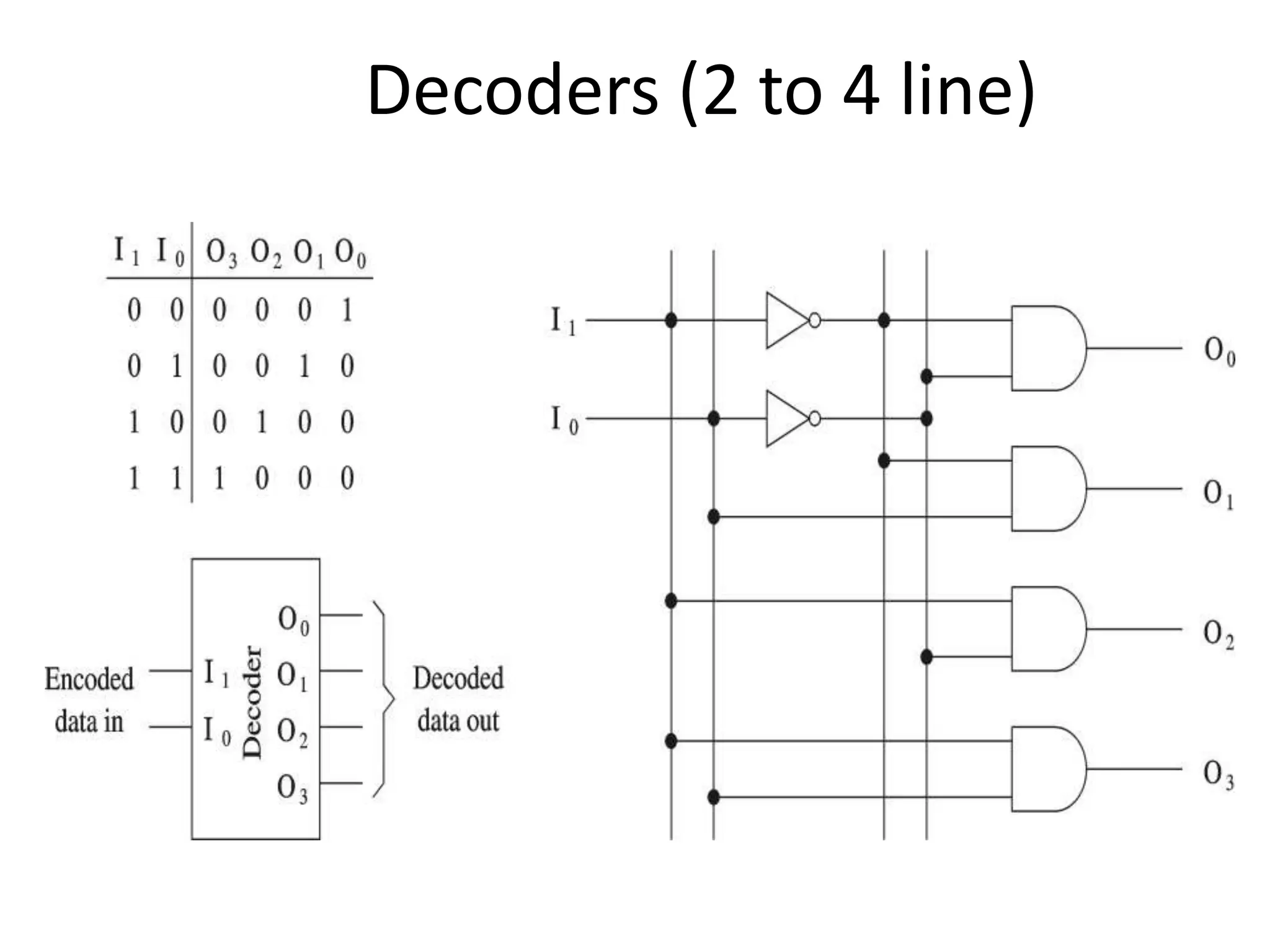
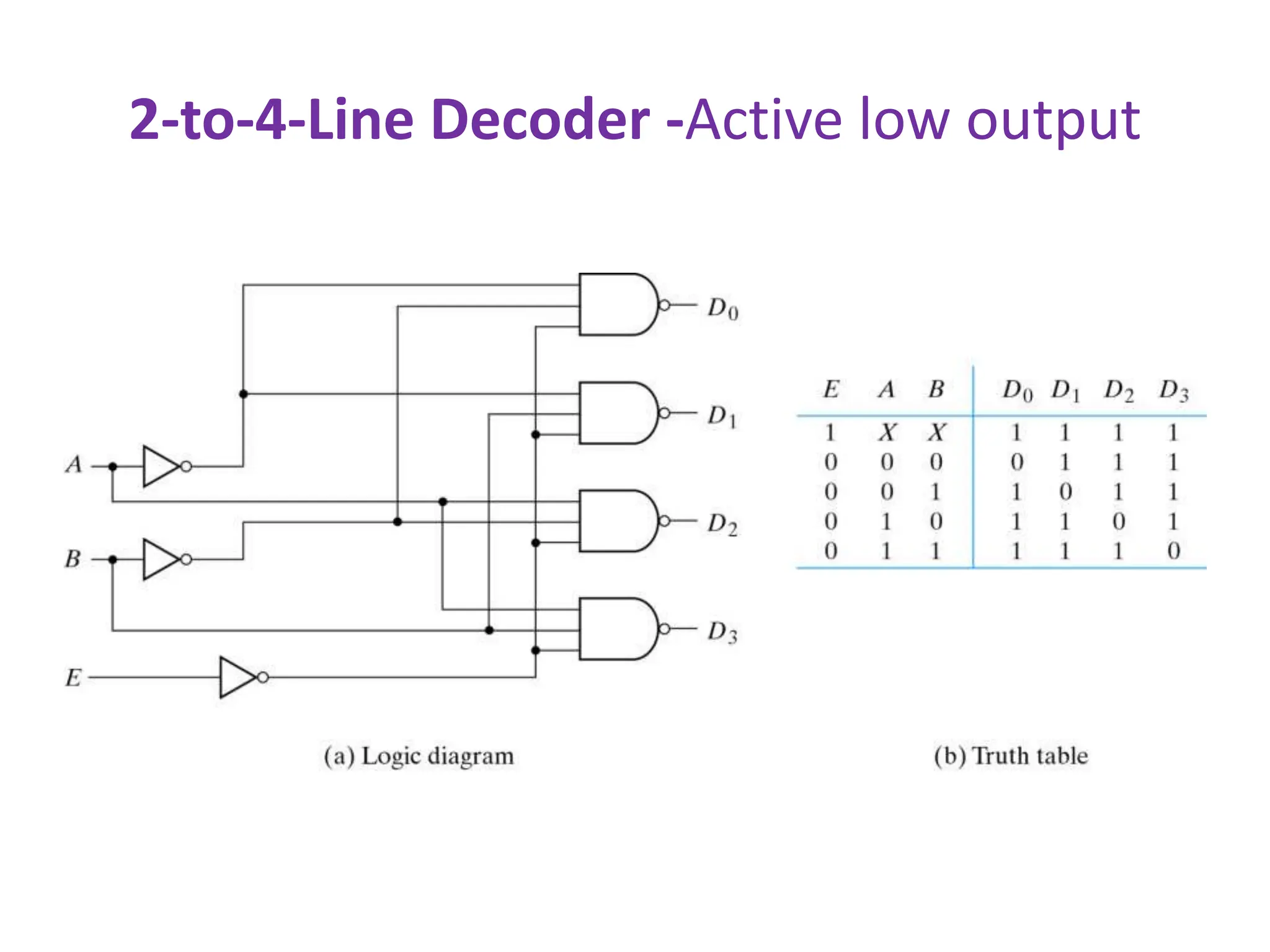

The document discusses the concepts of ripple-carry adders and carry look-ahead adders, explaining their mechanisms and delays in processing binary addition. It introduces the arithmetic logic unit (ALU), detailing its function in performing arithmetic and logical operations, as well as components like encoders and decoders used in digital circuits. Additionally, it describes the complexities associated with implementing CLA adders for larger bit sizes and presents examples of digital circuits including octal-to-binary encoders and BCD-to-decimal decoders.