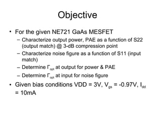
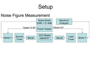
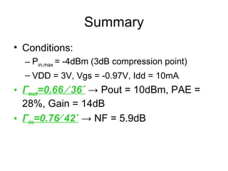
1. The document describes characterizing the output power, power added efficiency (PAE), and noise figure of a NE721 GaAs MESFET as a function of input and output matching conditions using load pull and noise figure measurements.
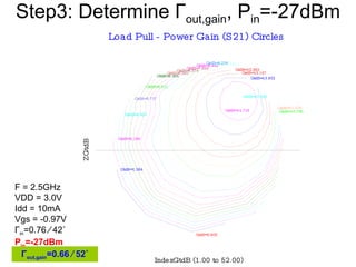
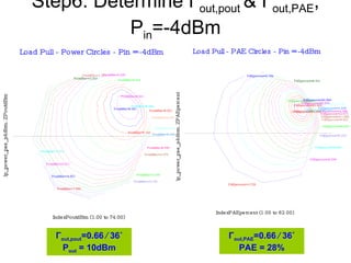
2. The optimum output match for gain is found to be Γout = 0.66/52° at Pin = -27dBm, but shifts to Γout = 0.66/36° at Pin = -4dBm (3dB compression point).
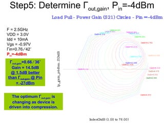
3. The optimum conditions are found to be Γout = 0.66/36° and Γin = 0.76/42° at Pin = -4dBm, producing


![RF Module Design - [Chapter 5] Low Noise Amplifier](https://cdn.slidesharecdn.com/ss_thumbnails/rfch5-150613070346-lva1-app6891-thumbnail.jpg?width=640&height=640&fit=bounds)