SlideShare a Scribd company logo
1 of 91
Stack Operation : Stack is a reserved portion of RAM set by the user.It works
on the principle of LIFO(last in first out).In 8085 MP there are two Instructions
related to stack operations PUSH and POP. PUSH instruction moves the
contents of register pair in to stack. The POP instruction moves the contents of
stack to register pair.
The stack is a LIFO (last in, first out) data structure implemented in the RAM
area and is used to store addresses and data when the microprocessor
branches to a subroutine. Then the return address used to get pushed on this
stack.
8085 has a special 16-bit register, holds the address of stack RAM called stack
pointer SP.
SP is a special purpose 16-bit register. It contains a memory address. Suppose
SP contents are FC78H, then the 8085 interprets it as follows.
Memory locations FC78H, FC79H, ..., FFFFH are having useful information. In
other words, these locations are treated as filled locations. Memory locations
FC77H, FC76H, ..., 0000H are not having any useful information. In other words,
these locations are treated as empty locations.
Unit 2: Stack Operation and Programming
• On a stack, we can perform two operations. PUSH and POP. In case of PUSH
operation, the SP register gets decreased by 2 and new data item used to
insert on to the top of the stack. On the other hand, in case of POP operation,
the data item will have to be deleted from the top of the stack and the SP
register will get increased by the value of 2.
• Thus, the contents of SP specify the top most useful location in the stack. In
other words, it indicates the memory location with the smallest address
having useful information. Fig. Interpretation of SP contents
Read and Write the stack in 8085 Microprocessor
• Reading from the Stack
• Let us consider that SP contents the address FC78H, and we want to read
information from a stack location. In this case, we are not interested in reading
from a location whose address is less than the memory address present in SP. This
is because 8085 interprets them as useless information. For example, there is no
point in reading useless information from memory location FC75H.
• SP interprets that, memory locations FC78H, FC79H, ..., FFFFH are all interpreted by
8085 to have useful information. To read from Stack, the instruction is POP in 8085
microprocessor instruction set. Here we shall discuss more about the POP
instruction below.
• In 8085 Instruction set, with the mnemonic POP, we can pop out 2-Bytes from the
top of the stack through rp i.e. register pair e.g. BC, DE, HL or AF. Here AF is a
register pair formed with Flag and Accumulator registers and also known as PSW
(Processor Status Word). In PSW, Accumulator is the MS Byte, and Flags register is
the LS Byte.
Mnemonics,
Operand
Opcode (in HEX) Bytes
POP B C1 1
POP D D1 1
POP H E1 1
POP PSW F1 1
rp Code Register Pair
0 0 BC
0 1 DE
1 0 HL
1 1 SP or PSW, but never both at
the same time.
• Let us consider the following example for a better understanding of the operation of the
instruction.Here we are considering the instruction POP D which is an instruction falling
in the category. As rp can have any of the four values, there are four opcodes for this type
of instruction. It occupies only 1-Byte in memory. POP D is an example of instruction of
this type. It is 1-Byte instruction. The result of the execution of this instruction is shown
below with an example.
Before
After
(BC) AABBH AABBH
(SP) 3FFEH 4000H
(3FFFH) AAH AAH
(3FFEH) BBH BBH
(DE) Any value AABBH
Address Hex Codes Mnemonic Comment
2000 01 LXI B, AABBH Initializing BC register pair with
AABBH
2001 BB Low order Byte BBH
2002 AA High order Byte AAH
2003 31 LXI SP,4000H Initializing SP with 4000H
2004 00 Low order Byte 00H
2005 40 High order Byte 40H
2006 C5 PUSH B At 3FFFH, AAH and at 3FFEH,
BBH will be moved
2007 D1 POP D Popping and initializing DE
register pair with stack
contents
The timing diagram against this instruction POP D execution is as follows –
• Writing to the Stack
• Let us consider that SP contents are FC7AH, and we want to write information to a
stack location. In this case, we are not interested in writing to a location whose
address is equal or greater than the memory address present in SP. This is because
the 8085 interprets them as having useful information, which should not be
destroyed! For example, there is no point in overwriting and destroying useful
information at memory location FD7AH. We should be writing into a location
where there is presently useless information, and make it useful.
• To write onto Stack, the instruction is PUSH in 8085 microprocessor instruction
set. Here we shall discuss more about the PUSH instruction below.
• In 8085 Instruction set, PUSH rp instruction stores contents of register pair rp by
pushing it into two locations above the top of the stack. rp stands for one of the
following register pairs.
• rp = BC, DE, HL, or PSW
• As rp can have any of the four values, there are four opcodes for this type of
instruction. It occupies only 1-Byte in memory.
Note : POP requires 1-Byte, 3-Machine Cycles (Opcode Fetch, Memory Read,
Memory Read) and 10 T-States for execution.
Mnemonics, Operand Opcode (in HEX) Bytes
PUSH B C5 1
PUSH D D5 1
PUSH H E5 1
PUSH PSW F5 1
In the above mention Opcodes, 2-bits are occupied to mention the register pair. 2-bits can have 4
combinations. So 4 register pairs can be mentioned with POP. As mentioned earlier, they are BC, DE,
HL, and AF or PSW.
Note with LXI instruction, we are having 4 possible register pairs can be used i.e. BC, DE, HL, and
SP. So at the same time, we can’t have SP and PSW applicable with the same instruction.
rp Code Register Pair
0 0 BC
0 1 DE
1 0 HL
1 1 SP or PSW, but never both at the same
time.
Let us consider PUSH B as an example of instruction of this category. It is 1-Byte
instruction. The result of the execution of this instruction is shown below with an
example.
Before After
(BC) AABBH AABBH
(SP) 4000H 3FFEH
(3FFFH) Any value AAH
(3FFEH) Any value BBH
Address Hex Codes Mnemonic Comment
2000 01 LXI B, AABBH Initializing BC register pair
with AABBH
2001 BB Low order Byte BBH
2002 AA High order Byte AAH
2003 31 LXI SP,4000H Initializing SP with 4000H
2004 00 Low order Byte 00H
2005 40 High order Byte 40H
2006 C5 PUSH B At 3FFFH, AAH and at 3FFEH,
BBH will be moved
Note : PUSH B requires 1-Byte, 3-Machine Cycles (Opcode Fetch-1MC, Memory Write-2 MC) and
12 T-States for execution.
SUBROUTINES:
• a subroutine is a sequence of program instructions that perform a specific
task, packaged as a unit. This unit can then be used in programs wherever
that particular task have to be performed. A subroutine is often coded so
that it can be started (called) several times and from several places during
one execution of the program, including from other subroutines, and then
branch back (return) to the next instruction after the call, once the
subroutine’s task is done. It is implemented by using Call and Return
instructions. The different types of subroutine instructions are
• Unconditional Call instruction –
CALL address is the format for unconditional call instruction. After execution
of this instruction program control is transferred to a sub-routine whose
starting address is specified in the instruction. Value of PC (Program Counter)
is transferred to the memory stack and value of SP (Stack Pointer) is
decremented by 2.
Conditional Call instruction – In these instructions program control is transferred to
subroutine and value of PC is pushed into stack only if condition is satisfied.
INSTRUCTION PARAMETER COMMENT
CC 16-bit address Call at address if cy (carry flag) = 1
CNC 16-bit address Call at address if cy (carry flag) = 0
CZ 16-bit address Call at address if ZF (zero flag) = 1
CNZ 16-bit address Call at address if ZF (zero flag) = 0
CPE 16-bit address Call at address if PF (parity flag) = 1
CPO 16-bit address Call at address if PF (parity flag) = 0
CN 16-bit address Call at address if SF (signed flag) = 1
CP 16-bit address Call at address if SF (signed flag) = 0
• Unconditional Return instruction – RET is the instruction used to mark the
end of sub-routine. It has no parameter. After execution of this instruction
program control is transferred back to main program from where it had
stopped. Value of PC (Program Counter) is retrieved from the memory stack
and value of SP (Stack Pointer) is incremented by 2.
• Conditional Return instruction – By these instructions program control is
transferred back to main program and value of PC is popped from stack only
if condition is satisfied. There is no parameter for return instruction.
INSTRUCTION COMMENT
RC Return from subroutine if cy (carry flag) = 1
RNC Return from subroutine if cy (carry flag) = 0
RZ Return from subroutine if ZF (zero flag) = 1
RNZ Return from subroutine if ZF (zero flag) = 0
RPE Return from subroutine if PF (parity flag) = 1
RPO Return from subroutine if PF (parity flag) = 0
RN Return from subroutine if SF (signed flag) = 1
RP Return from subroutine if SF (signed flag) = 0
• Advantages of Subroutine –
• Decomposing a complex programming task into simpler steps.
• Reducing duplicate code within a program.
• Enabling reuse of code across multiple programs.
• Improving tractability or makes debugging of a program easy.
LABEL OPCODE OPERAND COMMENTS T STATES
MVI C , FFH ; Load register C 7
Loop : DCR C ; Decrement C 4
JNZ LOOP ; Jump back to 10/7
decrement C Clock frequency of the system = 2 MHz Clock period= 1/T= 0.5 μs
Time to execute MVI = 7 T states * 0.5= 3.5 μs Time Delay in Loop TL= T*Loop
T states * N10 = 0.5 * 14* 255 = 1785 μs = 1.8 ms N10 = Equivalent decimal
number of hexadecimal count loaded in the delay register TLA= Time to
execute loop instructions =TL –(3T states* clock period)=1785-1.5=1783.5 μs
TIME DELAY USING A REGISTER PAIR :
Label Opcode Operand Comments T states
LXI B , 2384H Load BC with 16-bit count 10
LOOP : DCX B Decrement BC by 1 6
MOV A,C Place contents of C in A 4
ORA B OR B with C to set Zero flag 4
JNZ LOOP if result not equal to 0 , 10/7
jump back to loop Time Delay in Loop TL= T*Loop T states * N10 = 0.5 * 24* 9092 = 109 ms
Time Delay using a LOOP within a LOOP :
MVI B , 38H 7T
LOOP2: MVI C , FFH 7T
LOOP1: DCR C 4T
JNZ LOOP1 10/7 T
DCR B 4T
JNZ LOOP 2 10/7T
Delay in Loop TL1=1783.5 μs , Delay in Loop TL2= (0.5*21+TL1)*56 =100.46ms .
ILLUSTRATIVE PROGRAM: HEXADECIMAL COUNTER
Write a Program to count continuously from FFH to 00H using register C with
delay count 8CH between each count and display the number at one of the
output ports.
MVI B,00H
NEXT: DCR B
MVI C,8CH
DELAY: DCR C
JNZ DELAY
MOV A,B
OUT PORT#
JMP NEXT
ILLUSTRATIVE PROGRAM: ZERO TO NINE (MODULO TEN) COUNTER
START: MVI B,00H
MOV A,B
DSPLAY: OUT PORT #
LXI H,16-bit
LOOP: DCX H
MOV A,L
ORA H
JNZ LOOP
INR B
MOV A,B
CPI 0AH
JNZ DSPLAY
JZ START
Flow Chart: Start Initialize counter Display Output Load Delay register Decrement Delay
register Is Delay register=0? Next Count Is count =0AH? If yes, Initialize counter If no, Display
Output
Timing Diagram:
Timing Diagram is a graphical representation. It represents the execution time
taken by each instruction in a graphical format. The execution time is
represented in T- sates.It represents the clock cycle and duration, delay,
content of address bus and data bus, type of operation I e. Read/write/status
signals.
Machine Cycle:The time required to access the memory or input/output
devices is called machine cycle.
T-State:
Instruction Cycle: The time required to execute an instruction is called
instruction cycle.
The machine cycle and instruction cycle takes multiple clock
periods. A portion of an operation carried out in one system clock
period is called as T-state.
Machine cycles of 8085
The 8085 microprocessor has 5 (seven) basic machine cycles. They are
 Opcode fetch cycle (4T)
 Memory read cycle (3 T)
 Memory write cycle (3 T)
 I/O read cycle (3 T)
 I/O write cycle (3 T)
Signal 1.Opcode fetch machine cycle of 8085 :
Each instruction of the processor has one byte opcode.
 The opcodes are stored in memory. So, the processor
executes the opcode fetch machine cycle to fetch the
opcode from memory.
 Hence, every instruction starts with opcode fetch
machine cycle.
 The time taken by the processor to execute the opcode
fetch cycle is 4T.
 In this time, the first, 3 T-states are used for fetching the
opcode from memory and the remaining T-states are used
for internal operations by the processor.
2. Memory Read Machine Cycle of 8085:
 The memory read machine cycle is executed by
the processor to read a data byte from memory.
 The processor takes 3T states to execute this
cycle.
The instructions which have more than one byte
word size will use the machine cycle after the
opcode fetch machine cycle.
Cycle 3. Memory Write Machine Cycle of 8085
The memory write machine cycle is executed by the processor to
write a data byte in a memory location.
 The processor takes, 3T states to execute this machine cycle.
4. I/O Read Cycle of 8085
 The I/O Read cycle is executed by the processor to read a data
byte from I/O port or from the peripheral, which is I/O, mapped in
the system.
 The processor takes 3T states to execute this machine cycle.
 The IN instruction uses this machine cycle during the
execution.
Figure:I/O write timing diagram :
Operation:
•It is used to writ one byte into IO device.
•It requires 3 T-States.
•During T1, the lower byte of address is duplicated into higher order address bus A8-A15.
•ALE is high and A0-A7 address is selected from AD0-AD7.
•As it is an IO operation IO/M (bar) goes low.
•During T2, ALE goes low, WR (bar) goes low and data appears on AD0-AD7 to write data
into IO device.
•During T3, Data remains on AD0-AD7 till WR(bar) is low.
Examples:1. Timing diagram for STA 526AH
STA means Store Accumulator -The contents of the accumulator is stored in the specified
address (526A H).
The opcode of the STA instruction is said to be 32H. It is fetched from the memory 41FFH
(see fig). - OF machine cycle Then the lower order memory address is read (6AH). -
Memory Read Machine Cycle
Read the higher order memory address (52H).- Memory Read Machine Cycle
The combination of both the addresses are considered and the content from accumulator is
written in 526AH. - Memory Write Machine Cycle Assume the memory address for the
instruction and let the content of accumulator is C7H. So, C7H from accumulator is now
stored in 526AH.
2.Timing diagram for INR M:
Fetching the Opcode 34H from the memory 4105H. (OF
cycle).Let the memory address (M) be 4250H. (MR cycle -
To read Memory address and data).Let the content of that
memory is 12H.Increment the memory content from 12H
to 13H. (MW machine cycle)
MP 8085 Assembly Language Programming:
1. Store 8-bit data in memory using direct addressing:
• MVI A, 49H : "Store 49H in the accumulator"
• STA 2501H : "Copy accumulator contents at address 2501H"
• HLT : "Stop"
2. Store 8-bit data in memory using indirect addressing:
• LXI H : "Load H-L pair with 2501H"
• MVI M : "Store 49H in memory location pointed by H-
L register pair (2501H)"
• HLT : "Stop"
3. Data Transfer and memory operations (Direct and Indirect Addressing):
To write an Assembly Language Program to transfer a data block without
overlap using 8085
ALGORITHM: STEP 1: Load the DE pair with the destination address.
STEP 2: Load the HL pair with the count of elements in the data block.
STEP 3: Load element in the data block.
STEP 4: Increment the source address.
STEP 5: Copy the element to the accumulator and then transfer it to the
destination address.
STEP 6: Increment destination address.
STEP 7: Decrement the count.
STEP 8: If Count = 0 then go to the next step else go to step 3.
STEP 9: Terminate the program.
Flow Chart:
ALP : SOURCE CODE :
LABEL : MNEMONIC COMMENT
LXI D,4500 Load destination address in DE pair
LXI H,4100 Load the count in HL pair
MOV C,M Copy the count to register C
LOOP: INX H Increment memory
MOV A,M Copy element to Accumulator
STAX D Store the element to the address in the DE pair
INX D Increment destination address
DCR C Decrement count
JNZ LOOP Jump on non-zero to the label LOOP
HLT Program ends
Address Hex Codes Label Mnemonic T-States Comment
8000 11,50,80 START: LXI D, 8050H 10 Setup HL pair as a pointer for source
memory.
8003 21,70,80 LXI H, 8070H 10 Set up DE pair as a pointer for
destination memory
8006 4E MOV C , M 7 Set up B to count 16 bytes
8008 23 LOOP: INX H 7 Get data byte from source.
8009 7E MOV A,M 7 Store data byte as destination
800A 12 STAX D 6 Point HL to next source location
800B 13 INX D 6 Point DE to next destination
800C 0D DCR C 4 Decrement count
800D C2,08,80 JNZ LOOP 10 If counter is not 0, go back to
transfer next byte.
8010 76 HLT 5 Stop
4. Add two 8-bit numbers:
Example
(2501 H) = 99H (2502 H) = 39H Result (2503 H) = 99H + 39H = D2H
Since, 1 0 0 1 1 0 0 1 (99H) + 0 0 1 1 1 0 0 1 (39H) 1 1 0 1 0 0 1 0 (D2H)
Program
1.LXI H, 2501H : "Get address of first number in HL pair. Now
H-L points to 2501H"
2.MOV A, M : "Get first operand in accumulator"
3.INX H : "Increment content of HL pair. Now, HL points
2502H"
4.ADD M : "Add first and second operand"
5.INX H : "H-L points 4002H"
6.MOV M, A : "Store result at 2503H"
7.HLT : "Stop"
Subtract two 8-bit numbers:
Example
(2501 H) = 49H (2502 H) = 32H Result (2503 H) = 49H - 32H = 17H
Program
1.LXI H, 2501H : "Get address of first number in HL pair.
Now H-L points to 2501H"
2.MOV A, M : "Get first operand in accumulator"
3.INX H : "Increment content of HL pair. Now,
HL points 2502H"
4.SUB M : "Subtract first to second operand"
5.INX H : "H-L points 4002H"
6.MOV M, A : "Store result at 2503H"
7.HLT : "Stop"
5.Add two 16-bits numbers:
Add the 16-bit number in memory locations 2501H
and 2502H to the 16-bit number in memory
locations 2503H and 2504H. The most significant
eight bits of the two numbers to be
added are in memory locations 2502H and 4004H.
Store the result in memory locations 2505H and
2506H with the most significant byte in memory
location 2506H.
Example
(2501H) = 15H (2502H) = 1CH (2503H) = B7H (2504H) =
5AH Result = 1C15 + 5AB7H = 76CCH (2505H) = CCH
(2506H) = 76H
. Program :
• Add two 16-bits number with ADD and ADC instruction
• LHLD 2501H : "Get 1st 16-bit number in H-L pair"
• XCHG : "Save 1st 16-bit number in DE"
• LHLD 2503H : "Get 2nd 16-bit number in H-L pair"
• MOV A, E : "Get lower byte of the 1st number"
• ADD L : "Add lower byte of the 2nd number"
• MOV L, A : "Store result in L-register"
• MOV A, D : "Get higher byte of the 1st number"
• ADC H : "Add higher byte of the 2nd number with CARRY"
• MOV H, A : "Store result in H-register"
• SHLD 4004H : "Store 16-bit result in memory locations 2505H and 2506H"
• HLT : "Stop"
Add two 16-bits numbers with DAD instruction :
• LHLD 2501H : "Get 1st 16-bit number"
• XCHG : "Save 1st 16-bit number in DE"
• LHLD 2503H : "Get 2nd 16-bit number in H-L"
• DAD D : "Add DE and HL"
• SHLD 2505H : "Store 16-
bit result in memory locations 2505H and 2506H".
• HLT : "Stop"
Subtract two 16-bit numbers:
Example
(2500H) = 19H (2501H) = 6AH (2504H) = 15H (2503H) = 5CH Result = 6A19H ?
5C15H = OE04H (2504H) = 04H (2505H) = OEH
• Program:16-Bits Substraction:
• LHLD 2500H : "Get first 16-bit number in HL"
• XCHG : "Save first 16-bit number in DE"
• LHLD 2502H : "Get second 16-bit number in HL"
• MOV A, E : "Get lower byte of the first number"
• SUB L : "Subtract lower byte of the second number"
• MOV L, A : "Store the result in L register"
• MOV A, D : "Get higher byte of the first number"
• SBB H : "Subtract higher byte of second number with borrow"
• MOV H, A : "Store l6-bit result in memory locations 2504H and 2505H"
• SHLD 2504H : "Store l6-bit result in memory locations 2504H and 2505H"
• HLT : "Terminate program execution"
ADD CONTENTS OF TWO MEMORY LOCATIONS:
Example
(2500H) = 7FH (2501H) = 89H Result = (2502H) = 08H (2503H) = 01H
Program
1.LXI H, 2500H : "HL Points 2500H"
2.MOV A, M : "Get first operand"
3.INX H : "HL Points 2501H"
4.ADD M : "Add second operand"
5.INX H : "HL Points 2502H"
6.MOV M, A : "Store the lower byte of result at 2502H"
7.MVIA, 00 : "Initialize higher byte result with 00H"
8.ADC A : "Add carry in the high byte result"
9.INX H : "HL Points 2503H"
10.MOV M, A : "Store the higher byte of result at 2503H"
11.HLT : "Terminate program execution"
To perform the multiplication of two 8 bit numbers using 8085:
ALGORITHM 1) Start the program by loading HL register pair with address of memory
location.
2) Move the data to a register (B register).
3) Get the second data and load into Accumulator.
4) Add the two register contents.
5) Check for carry.
6) Increment the value of carry.
7) Check whether repeated addition is over and store the value of product and carry in
memory location.
8) Terminate the program.
SOURCE CODE
MVI D, 00 Initialize register D to 00
MVI A, 00 Initialize Accumulator content to 00
LXI H, 4150
MOV B, M Get the first number in B - reg
INX H
MOV C, M Get the second number in C- reg.
LOOP: ADD B Add content of A - reg to register B.
JNC NEXT Jump on no carry to NEXT.
INR D Increment content of register D
NEXT: DCR C Decrement content of register C.
JNZ LOOP Jump on no zero to address
STA 4152 Store the result in Memory
MOV A, D Move the content of D register to Accumulator
STA 4153 Store the MSB of result in Memory
HLT Terminate the program.
Input : FF (4150) FF (4151)
Output: 01 (4152) FE (4153)
To perform the division of two 8 bit numbers using 8085:
ALGORITHM :
1) Start the program by loading HL register pair with address of memory location.
2) Move the data to a register (B register).
3) Get the second data and load into Accumulator.
4) Compare the two numbers to check for carry.
5) Subtract the two numbers.
6) Increment the value of carry.
7) Check whether repeated subtraction is over and store the value of product and
carry in memory location.
8) Terminate the program.
SOURCE CODE:
LXI H, 4150
MOV B, M Get the dividend in B – reg.
MVI C, 00 Clear C – reg for quotient
INX H
MOV A, M Get the divisor in A – reg.
NEXT: CMP B Compare A - reg with register B.
JC LOOP Jump on carry to LOOP
SUB B Subtract A – reg from B- reg.
INR C Increment content of register C.
JMP NEXT Jump to NEXT
LOOP: STA 4152 Store the remainder in Memory
MOV A, C Move the Content of C register to Accumulator
STA 4153 Store the quotient in memory
HLT Terminate the program.
Input: FF (4150) FF (4251) Output: 01 (4152) - Remainder FE (4153) - Quotient RESULT
Thus the program to divide two 8-bit numbers was executed.
To find the largest number in an array of data using 8085 instruction set:
ALGORITHM
STEP 1: Load the address of the first element of the array in HL pair
STEP 2: Move the count to B – reg.
STEP 3: Increment the pointer
STEP 4: Get the first data in A – reg.
STEP 5: Decrement the count.
STEP 6: Increment the pointer
STEP 7: Compare the content of memory addressed by HL pair with that of A - reg.
STEP 8: If Carry = 0, go to step 10 or if Carry = 1 go to step
9 STEP 9: Move the content of memory addressed by HL to A – reg.
STEP 10: Decrement the count
STEP 11: Check for Zero of the count. If ZF = 0, go to step 6, or if ZF = 1 go to next
step.
STEP 12: Store the largest data in memory. STEP 13: Terminate the program.
SOURCE CODE:
LXI H,4200 Set pointer for array
MOV B,M Load the Count
INX H
MOV A,M Set 1st element as largest data
DCR B Decrement the count
LOOP: INX H
CMP M If A- reg > M go to AHEAD
JNC AHEAD
MOV A,M Set the new value as largest
AHEAD: DCR B
JNZ LOOP Repeat comparisons till count = 0
STA 4300 Store the largest value at 4300
HLT
Input: 05 (4200) -- Array Size 0A (4201) F1 (4202) 1F (4203) 26 (4204) FE (4205)
Output: FE (4300) RESULT
Thus the program to find the largest number in an array of data was executed
To find the smallest number in an array of data using 8085 instruction set:
ALGORITHM:
STEP 1: Load the address of the first element of the array in HL pair
STEP 2: Move the count to B – reg.
STEP 3: Increment the pointer
STEP 4: Get the first data in A – reg.
STEP 5: Decrement the count.
STEP 6: Increment the pointer
STEP 7: Compare the content of memory addressed by HL pair with that of A - reg.
STEP 8: If carry = 1, go to step 10 or if Carry = 0 go to step 9
STEP 9: Move the content of memory addressed by HL to A – reg.
STEP 10: Decrement the count
STEP 11: Check for Zero of the count. If ZF = 0, go to step 6, or if ZF = 1 go to next
step.
STEP 12: Store the smallest data in memory. STEP 13: Terminate the program.
SOURCE CODE :
LXI H,4200 Set pointer for array
MOV B,M Load the Count
INX H
MOV A,M Set 1st element as largest data
DCR B Decrement the count
LOOP: INX H
CMP M If A- reg < M go to AHEAD
JC AHEAD
MOV A,M Set the new value as smallest
AHEAD: DCR B
JNZ LOOP Repeat comparisons till count = 0
STA 4300 Store the largest value at 4300
HLT
Input: 05 (4200) - Array Size 0A (4201) F1 (4202) 1F (4203) 26 (4204) FE (4205)
Output: 0A (4201) RESULT
Thus the program to find the smallest number in an array of data was executed
WRITE AN ALP TO SORT THE SERIES IN ASCENDING ORDER:
Algorithm: 1.Initialize the source memory pointer.
2.Initialize two counters: one to compare the data and another to repeat the
process of comparison till all the nos. are over.
3.The first and the next no. are compared. Smaller of the two is retained in the
first memory location. The larger of the two is moved to the next memory
location.
4.Decrement the count.
5.The second memory location is compared with the third and again step 3 is
repeated till the count is zero.
6.At the end, the largest number will be at the last location.
Data: N no. of bytes stored from 2201 onwards.
Result: Numbers stored from 2201 are arranged in ascending order.
Sample: N=(2200), source location: 2201 to 2205,
destination location: 2201 to 2205
Memory Addr. Opcode/ data Label Mnemonics Comments
7000,01,02 3A,00,22 LDA 2200H Load Acc with the count
7003 47 MOV B, A Save count to reg B.
7004,05,06 21,01,22 LOOP2 LXI H, 2201H Initialize HL pair with
source memory.
7007 48 MOV C, B Initialize C with count
7008 7E LOOP1 MOV A, M Transfer src data to reg.A.
7009 23 INX H Increment HLpair by 1
700A BE CMP M Compare the two nos.
700B,0C,0D DA,13,70 JC DOWN If no.1<no.2,go to Label
DOWN
700E 56 MOV D,M Save smaller no. in D
700F 77 MOV M,A Larger no. in II memory
location.
Memory Addr. Opcode/ data Label Mnemonics Comments
7010 2B DCX H Decrement HL
7011 72 MOVM,D Save smaller no. in I memory
location.
7012 23 INX H Increment HL to point to next
memory location.
7013 0D DOWN DCR C Decrement count by
7014,15,16 C2,08,70 JNZ LOOP1 If not zero, jump to loop1
7017 05 DCR B Decrement count by1
7018,19,1A C2,04,70 JNZ LOOP2 If not zero, jump to loop2
701B CF RST1 Stop Conclusion:
Thus, program written for arranging numbers in ascending order is successfully
executed.
Program to arrange an array of data in descending order using 8085.
Algorithm :
1) Initialize HL pair as memory pointer.
2) Get the count at 4200 in to C register.
3) Copy it in D register.
4) Get the first vale in Accumulator.
5) Compare it with the value at next location.
6) If they are out of order, exchange the contents of accumulator and
memory.
7) Decrement D register’s content by 1.
8) Repeat steps 5 and 7 till the value in D register become zero.
9) Decrement C register’s content by 1.
10) Repeat steps 3 to 9 till the value in C register becomes zero.
11) Terminate the program.
Program
:
MEMORY LABEL MNEMONIC HEX CODE COMMENT
4400 LXI H,4200 21,00,42 Load the array size to the HL pair
4403 MOV C,M 4E Copy the array size to C register
4404 DCR C 0D Decrement C by 1
4405 REPEAT MOV D,C 51 Copy content of C to D register
4406 LXI H,4201 21,01,42 Load the first data to the HL pair
4409 LOOP MOV A,M 7E Copy the data to the accumulator
440A INX H 23 Increment memory by 1
440B CMP M BE Compare accumulator and memory
content
440C JNC SKIP D2,14,44 Jump on no carry to the label SKIP
440F MOV B,M 46 Copy memory content to B register
4410 MOV M,A 77 Copy accumulator content to memory
4411 DCX H 2B Decrement memory by 1
MEMORY LABEL MNEMONIC HEX CODE COMMENT
4412 MOV M,B 70 Copy B register’s content to memory
4413 INX H 23 Increment memory by 1
4414 SKIP DCR D 15 Decrement D by 1
4415 JNZ LOOP C2,09,44 Jump on non-zero to the label LOOP
4418 DCR C 0D Decrement C by 1
4419 JNZ REPEAT C2,05,44 Jump on non-zero to the label REPEAT
441C HLT 76 Program ends
Input at 4200 : 05H (Array Size)
4201 : 01H
4202 : 02H
4203 : 03H
4204 : 04H
4205 : 05H
Output at 4200 : 05H (Array Size)
4201 : 05H
4202 : 04H
4203 : 03H
4204 : 02H
4205 : 01H
Program to Add two multi-byte numbers in 8085 Microprocessor
We are using 4-byte numbers. The numbers are stored into the memory at location
8501H and 8505H. One additional information is stored at location 8500H. In this
place we are storing the byte count. The result is stored at location 85F0H.
The HL pair is storing the address of first operand bytes, the DE is storing the
address of second operand bytes. C is holding the byte count. We are using stack
to store the intermediate bytes of the result. After completion of the addition
operation, we are popping from the stack and storing into the destination.
Input: 8500H = 04H=Byte Count.
First number in memory loc :8501H=19H , 8502H=68H , 8503H=12H , 8504H=85.
Second number in memory loc:8505H=88H,8506H=25H,8507H=17H,8508H=20H.
Flow Diagram: Multi Byte Addition
Program:
Address HEX Codes Labels Mnemonics Comments
F000 31, 00, 20 LXI SP,2000H Initialize Stack
Pointer
F003 21, 00, 85 LXI H,8500H load memory
address to get byte
count
F006 4E MOV C,M load memory
content into C
register
F007 06, 00 MVI B,00H clear B register
F009 21, 01, 85 LXI H, 8501H load first argument
address
F00C 11, 05, 85 LXI D, 8505H load second
argument address
Address HEX Codes Labels Mnemonics Comments
F00F 1A LOOP LDAX D load DE with second
operand address
F010 8E ADC M Add memory content
and carry with Acc
F011 F5 PUSH PSW Store the accumulator
content into stack
F012 04 INR B increase b after pushing
into stack
F013 23 INX H Increase HL pair to point
next address
F014 13 INX D Increase DE pair to point
next address
F015 0D DCR C Decrease c to while all
bytes are not exhausted
Address HEX Codes Labels Mnemonics Comments
F016 C2, 0F, F0 JNZ LOOP When bytes are not
considered, loop again
F019 D2, 20, F0 JNC SKIP when carry = 0, jump to
store
F01C 3E, 01 MVI A,01H when carry = 1, push it
into stack
F01E F5 PUSH PSW Store the accumulator
content into stack
F01F 04 INR B increase b after
pushing into stack
F020 21, F0, 85 SKIP LXI H,85F0H load the destination
pointer
F023 F1 L1 POP PSW pop AF to get back
bytes from stack
Address HEX Codes Labels Mnemonics Comments
F024 77 MOV M,A store Acc data at
memory location
pointed by HL
F025 23 INX H Increase HL pair to
point next address
F026 05 DCR B Decrease B
F027 C2, 23, F0 JNZ L1 Go to L1 to store stack
contents
F02A 76 HLT Terminate the program
Output
Output : 85F0=00 , 85F1=A5 , 85F2=29 , 85F3=8D , 85F4=A1
program to find 1’s and 2’s complement of 8-bit number:
MEMORY MNEMONICS OPERANDS COMMENT
2000 LDA [3000] [A] <- [3000]
2003 CMA [A] <- [A^]
2004 STA [3001] 1’s complement
2007 ADI 01 [A] <- [A] + 01
2009 STA [3002] 2’s complement
200C HLT Stop
Algorithm –
1.Load the data from memory 3000 into A (accumulator)
2.Complement content of accumulator
3.Store content of accumulator in memory 3001 (1’s complement)
4.Add 01 to Accumulator content
5.Store content of accumulator in memory 3002 (2’s complement)
6.Stop
Program –
program to find the factorial of a number:
Algorithm –
1.Load the data into register B
2.To start multiplication set D to 01H
3.Jump to step 7
4.Decrements B to multiply previous number
5.Jump to step 3 till value of B>0
6.Take memory pointer to next location and store result
7.Load E with contents of B and clear accumulator
8.Repeatedly add contents of D to accumulator E times
9.Store accumulator content to D
10.Go to step 4
Explanation –
1.First set register B with data.
2.Set register D with data by calling MULTIPLY subroutine one time.
3.Decrement B and add D to itself B times by calling MULTIPLY subroutine as 4*3 is
equivalent to 4+4+4 (i.e., 3 times).
4.Repeat the above step till B reaches 0 and then exit the program.
5.The result is obtained in D register which is stored in memory
ADDRESS LABEL MNEMONIC COMMENT
2000H Data Data Byte
2001H Result Result of factorial
2002H LXI H, 2000H Load data from memory
2005H MOV B, M Load data to B register
2006H MVI D, 01H Set D register with 1
2008H FACTORIAL CALL MULTIPLY
Subroutine call for
multiplication
200BH DCR B Decrement B
200CH JNZ FACTORIAL
Call factorial till B becomes
0
200FH INX H Increment memory
2010H MOV M, D Store result in memory
ADDRESS LABEL MNEMONIC COMMENT
2011H HLT Halt
2100H MULTIPLY MOV E, B Transfer contents of B to C
2101H MVI A, 00H
Clear accumulator to store
result
2103H MULTIPLYLOOP ADD D Add contents of D to A
2104H DCR E Decrement E
2105H JNZ MULTIPLYLOOP Repeated addition
2108H MOV D, A Transfer contents of A to D
2109H RET Return from subroutine
Example – Assume Fibonacci series is stored at starting memory location 3050.
Note – This program generates Fibonacci series in hexadecimal numbers.
8085 program to generate Fibonacci series
Algorithm – For Fibonacci Series
1.Initialize register H with 30 and register L with 50, so that indirect memory
M points to memory location 3050.
2.Initialize register B with 00, register C with 08 and register D with 01.
3.Move the content of B in M.
4.Increment M by 1 so that M points to next memory location.
5.Move the content of D in M.
6.Move the content of B in accumulator A.
7.Add the content of D in A.
8.Move the content of D in B.
9.Move the content of A in D.
10.Increment M by 1 so that M points to next memory location.
11.Move the content of A in M.
12.Decrements C by 1.
13.Jump to memory location 200C if ZF = 0 otherwise Halt the program.
Program – For Fibonacci Series:
MEMORY ADDRESS MNEMONICS COMMENT
2000 LXI H, 3050 H <- 30, L <- 50
2003 MVI C, 08 C <- 08
2005 MVI B, 00 B <- 00
2007 MVI D, 01 D <- 01
2009 MOV M, B M <- B
200A INX H M <- M + 01
200B MOV M, D M <- D
200C MOV A, B A <- B
MEMORY ADDRESS MNEMONICS COMMENT
200D ADD D A <- A + D
200E MOV B, D B <- D
200F MOV D, A D <- A
2010 INX H M <- M + 01
2011 MOV M, A M <- A
2012 DCR C C <- C – 01
2013 JNZ 200C Jump if ZF = 0
2016 HLT END
find 1’s and 2’s complement of 16-bit number:
Algorithm –
1.Load a 16-bit number from memory 3000 into a register pair (H-L)
2.Move content of register L to accumulator
3.Complement content of accumulator
4.Move content of accumulator to register L
5.Move content of register H to accumulator
6.Complement content of accumulator
7.Move content of accumulator to register H
8.Store content of register pair in memory 3002 (1’s complement)
9.Increment content of register pair by 1
10.Store content of register pair in memory 3004 (2’s complement)
11.Stop
MEMORY MNEMONICS OPERANDS COMMENT
2000 LHLD [3000] [H-L] <- [3000]
2003 MOV A, L [A] <- [L]
2004 CMA [A] <- [A^]
2005 MOV L, A [L] <- [A]
2006 MOV A, H [A] <- [H]
2007 CMA [A] <- [A^]
2008 MOV H, A [H] <- [A]
2009 SHLD [3002] 1’s complement
200C INX H [H-L] <- [H-L] + 1
200D SHLD [3004] 2’s complement
2010 HLT Stop
Program – 1s and 2s Comlement of 16- bits Number:
Program for Number of 1s and 0s in a Byte:
Write a program to count number of ones in the given 8-bit number
use register B to display the count of ones where starting address
is 2000 and the number is stored at 3000 memory address and store
result into 3001 memory address.
Example:
Algorithm –
1.Move 00 to register B immediately for count
2.Move 08 to register C immediately for shifting
3.Load the data of memory [3000] into accumulator
4.Rotate ‘A’ right with carry
5.Jump if no carry to step-7
6.Otherwise increase register B by 1
7.Decrease register C by 1
8.Jump if not zero to step-4
9.Move content of register B into accumulator
10.Store content of accumulator into memory [3001] (number of
count)
11.Stop
Program –To count number of 1s and zeros in a byte:
MEMORY MNEMONICS OPERANDS COMMENT
2000 MVI B, 00 [B] <- 00
2002 MVI C, 08 [C] <- 08
2004 LDA [3000] [A] <- [3000]
2007 RAR rotate ‘A’ right with carry
2008 JNC 200C jump if no carry
200B INR B [B] <- [B] + 1
200C DCR C [C] <- [C] – 1
200D JNZ 2007 jump if not zero
2010 MOV A, B [A] <- [B]
2011 STA [3001] number of ones
2014
2016
2017
201A
MVI
SUB
STA
HLT
A,08
B
[3002]
[C]=[08]
[A]=[08]-[B]
Number of zeros
Stop
Explanation – Registers A, B and C are used for general purpose.
1.MVI is used to load an 8-bit given register immediately (2 Byte instruction)
2.LDA is used to load accumulator direct using 16-bit address (3 Byte instruction)
3.MOV is used to transfer the data from accumulator to register(any) or
register(any) to accumulator (1 Byte)
4.RAR is used to shift ‘A’ right with carry (1 Byte instruction)
5.STA is used to store data from accumulator into memory direct using 16-bit
address (3 Byte instruction)
6.INR is used to increase given register by 1 (1 Byte instruction)
7.JNC is used to jump to the given step if their is no carry (3 Byte instruction)
8.JNZ is used to jump to the given step if their is not zero (3 Byte instruction)
9.DCR is used to decrease given register by 1 (1 Byte instruction)
10.HLT is used to halt the program
Thank you

More Related Content

What's hot

Unit 6 assembly language programming
Unit 6   assembly language programmingUnit 6   assembly language programming
Unit 6 assembly language programmingKartik Sharma
 
Subroutine in 8051 microcontroller
Subroutine in 8051 microcontrollerSubroutine in 8051 microcontroller
Subroutine in 8051 microcontrollerbhadresh savani
 
Assembly Language Programming By Ytha Yu, Charles Marut Chap 8 (The Stack and...
Assembly Language Programming By Ytha Yu, Charles Marut Chap 8 (The Stack and...Assembly Language Programming By Ytha Yu, Charles Marut Chap 8 (The Stack and...
Assembly Language Programming By Ytha Yu, Charles Marut Chap 8 (The Stack and...Bilal Amjad
 
Unit 3 – assembly language programming
Unit 3 – assembly language programmingUnit 3 – assembly language programming
Unit 3 – assembly language programmingKartik Sharma
 
Stack in 8085 microprocessor
Stack in 8085 microprocessorStack in 8085 microprocessor
Stack in 8085 microprocessorhepzijustin
 
8051 assembly programming
8051 assembly programming8051 assembly programming
8051 assembly programmingsergeiseq
 
Assembly language programming_fundamentals 8086
Assembly language programming_fundamentals 8086Assembly language programming_fundamentals 8086
Assembly language programming_fundamentals 8086Shehrevar Davierwala
 
8051 addressing modes
 8051 addressing modes 8051 addressing modes
8051 addressing modesghoshshweta
 
Addressing modes of 8051
Addressing modes of 8051Addressing modes of 8051
Addressing modes of 8051SARITHA REDDY
 
Introduction to debugging linux applications
Introduction to debugging linux applicationsIntroduction to debugging linux applications
Introduction to debugging linux applicationscommiebstrd
 
Assembly Language Lecture 1
Assembly Language Lecture 1Assembly Language Lecture 1
Assembly Language Lecture 1Motaz Saad
 

What's hot (19)

Unit 6 assembly language programming
Unit 6   assembly language programmingUnit 6   assembly language programming
Unit 6 assembly language programming
 
8051assembly language
8051assembly language8051assembly language
8051assembly language
 
Lec04
Lec04Lec04
Lec04
 
Addressing modes
Addressing modesAddressing modes
Addressing modes
 
Subroutine in 8051 microcontroller
Subroutine in 8051 microcontrollerSubroutine in 8051 microcontroller
Subroutine in 8051 microcontroller
 
8086 assembly
8086 assembly8086 assembly
8086 assembly
 
8086 alp
8086 alp8086 alp
8086 alp
 
Assembly Language Programming By Ytha Yu, Charles Marut Chap 8 (The Stack and...
Assembly Language Programming By Ytha Yu, Charles Marut Chap 8 (The Stack and...Assembly Language Programming By Ytha Yu, Charles Marut Chap 8 (The Stack and...
Assembly Language Programming By Ytha Yu, Charles Marut Chap 8 (The Stack and...
 
Unit 3 – assembly language programming
Unit 3 – assembly language programmingUnit 3 – assembly language programming
Unit 3 – assembly language programming
 
Stack in 8085 microprocessor
Stack in 8085 microprocessorStack in 8085 microprocessor
Stack in 8085 microprocessor
 
Assembly 8086
Assembly 8086Assembly 8086
Assembly 8086
 
8051 assembly programming
8051 assembly programming8051 assembly programming
8051 assembly programming
 
Assembly language programming_fundamentals 8086
Assembly language programming_fundamentals 8086Assembly language programming_fundamentals 8086
Assembly language programming_fundamentals 8086
 
8051 addressing modes
 8051 addressing modes 8051 addressing modes
8051 addressing modes
 
8086 Microprocessor
8086 Microprocessor8086 Microprocessor
8086 Microprocessor
 
Addressing modes of 8051
Addressing modes of 8051Addressing modes of 8051
Addressing modes of 8051
 
Emu8086
Emu8086Emu8086
Emu8086
 
Introduction to debugging linux applications
Introduction to debugging linux applicationsIntroduction to debugging linux applications
Introduction to debugging linux applications
 
Assembly Language Lecture 1
Assembly Language Lecture 1Assembly Language Lecture 1
Assembly Language Lecture 1
 

Similar to B sc e 5.2 mp unit 2 soft ware(alp)

(a)Suppose the main memory of the Pep8 were completely filled with .docx
(a)Suppose the main memory of the Pep8 were completely filled with .docx(a)Suppose the main memory of the Pep8 were completely filled with .docx
(a)Suppose the main memory of the Pep8 were completely filled with .docxajoy21
 
Stacks & subroutines 1
Stacks & subroutines 1Stacks & subroutines 1
Stacks & subroutines 1deval patel
 
T imingdiagram
T imingdiagramT imingdiagram
T imingdiagrampuja00
 
Microprocessors-based systems (under graduate course) Lecture 7 of 9
Microprocessors-based systems (under graduate course) Lecture 7 of 9 Microprocessors-based systems (under graduate course) Lecture 7 of 9
Microprocessors-based systems (under graduate course) Lecture 7 of 9 Randa Elanwar
 
Addressing Modes
Addressing ModesAddressing Modes
Addressing ModesMayank Garg
 
8051 Programming (1).pptx
8051 Programming (1).pptx8051 Programming (1).pptx
8051 Programming (1).pptxDhyeayaParmar
 
Basic programming of 8085
Basic programming of 8085 Basic programming of 8085
Basic programming of 8085 vijaydeepakg
 
instruction-set-of-8086-mr-binu-joy3.ppt
instruction-set-of-8086-mr-binu-joy3.pptinstruction-set-of-8086-mr-binu-joy3.ppt
instruction-set-of-8086-mr-binu-joy3.pptssuser2b759d
 
8051 instruction set
8051 instruction set8051 instruction set
8051 instruction setStefan Oprea
 
Computer Organization and 8085 microprocessor notes
Computer Organization and 8085 microprocessor notesComputer Organization and 8085 microprocessor notes
Computer Organization and 8085 microprocessor notesLakshmi Sarvani Videla
 
Micro controller(pratheesh)
Micro controller(pratheesh)Micro controller(pratheesh)
Micro controller(pratheesh)Pratheesh Pala
 
Programming basic computer
Programming basic computerProgramming basic computer
Programming basic computerMartial Kouadio
 
Instruction set summary
Instruction set summary Instruction set summary
Instruction set summary janicetiong
 
Microprocessor architecture II
Microprocessor architecture   IIMicroprocessor architecture   II
Microprocessor architecture IIDr.YNM
 

Similar to B sc e 5.2 mp unit 2 soft ware(alp) (20)

Stack and subroutine
Stack and subroutineStack and subroutine
Stack and subroutine
 
Lec04
Lec04Lec04
Lec04
 
(a)Suppose the main memory of the Pep8 were completely filled with .docx
(a)Suppose the main memory of the Pep8 were completely filled with .docx(a)Suppose the main memory of the Pep8 were completely filled with .docx
(a)Suppose the main memory of the Pep8 were completely filled with .docx
 
Chapter 9
Chapter 9Chapter 9
Chapter 9
 
Stacks & subroutines 1
Stacks & subroutines 1Stacks & subroutines 1
Stacks & subroutines 1
 
T imingdiagram
T imingdiagramT imingdiagram
T imingdiagram
 
Microprocessors-based systems (under graduate course) Lecture 7 of 9
Microprocessors-based systems (under graduate course) Lecture 7 of 9 Microprocessors-based systems (under graduate course) Lecture 7 of 9
Microprocessors-based systems (under graduate course) Lecture 7 of 9
 
Addressing Modes
Addressing ModesAddressing Modes
Addressing Modes
 
8051 Programming (1).pptx
8051 Programming (1).pptx8051 Programming (1).pptx
8051 Programming (1).pptx
 
12 mt06ped008
12 mt06ped008 12 mt06ped008
12 mt06ped008
 
Basic programming of 8085
Basic programming of 8085 Basic programming of 8085
Basic programming of 8085
 
Lecture5
Lecture5Lecture5
Lecture5
 
instruction-set-of-8086-mr-binu-joy3.ppt
instruction-set-of-8086-mr-binu-joy3.pptinstruction-set-of-8086-mr-binu-joy3.ppt
instruction-set-of-8086-mr-binu-joy3.ppt
 
8051 instruction set
8051 instruction set8051 instruction set
8051 instruction set
 
Computer Organization and 8085 microprocessor notes
Computer Organization and 8085 microprocessor notesComputer Organization and 8085 microprocessor notes
Computer Organization and 8085 microprocessor notes
 
Micro controller(pratheesh)
Micro controller(pratheesh)Micro controller(pratheesh)
Micro controller(pratheesh)
 
Programming basic computer
Programming basic computerProgramming basic computer
Programming basic computer
 
6.pptx
6.pptx6.pptx
6.pptx
 
Instruction set summary
Instruction set summary Instruction set summary
Instruction set summary
 
Microprocessor architecture II
Microprocessor architecture   IIMicroprocessor architecture   II
Microprocessor architecture II
 

More from MahiboobAliMulla

More from MahiboobAliMulla (20)

B sc vi sem unit 2
B sc vi sem unit 2B sc vi sem unit 2
B sc vi sem unit 2
 
B sc vi sem e6.1 p1 unit 1
B sc vi sem e6.1 p1 unit 1B sc vi sem e6.1 p1 unit 1
B sc vi sem e6.1 p1 unit 1
 
B sc iv sem unit 3
B sc iv sem unit 3B sc iv sem unit 3
B sc iv sem unit 3
 
B sc iv sem unit 2 (2)
B sc iv sem unit 2 (2)B sc iv sem unit 2 (2)
B sc iv sem unit 2 (2)
 
B sc iv sem unit 1
B sc iv sem unit 1B sc iv sem unit 1
B sc iv sem unit 1
 
B sc ii sem unit 2(b) ba
B sc ii sem unit 2(b) baB sc ii sem unit 2(b) ba
B sc ii sem unit 2(b) ba
 
B sc ii sem unit 1
B sc ii sem unit 1B sc ii sem unit 1
B sc ii sem unit 1
 
B sc ii sem unit 2(a) ns
B sc ii sem  unit 2(a) nsB sc ii sem  unit 2(a) ns
B sc ii sem unit 2(a) ns
 
E5.1 commn unit 2 md
E5.1 commn unit 2 mdE5.1 commn unit 2 md
E5.1 commn unit 2 md
 
B sc e5.2 mp unit 4 mc-8051
B sc e5.2 mp unit 4 mc-8051B sc e5.2 mp unit 4 mc-8051
B sc e5.2 mp unit 4 mc-8051
 
B sc e5.2 mp unit 3 interfacing
B sc e5.2 mp unit 3 interfacingB sc e5.2 mp unit 3 interfacing
B sc e5.2 mp unit 3 interfacing
 
B sc e5.2 mp unit-1 hard ware
B sc e5.2 mp  unit-1 hard wareB sc e5.2 mp  unit-1 hard ware
B sc e5.2 mp unit-1 hard ware
 
B sc3 unit 5 sequencial lc
B sc3 unit 5 sequencial lcB sc3 unit 5 sequencial lc
B sc3 unit 5 sequencial lc
 
B sc3 unit 4 combi..lckt
B sc3 unit 4 combi..lcktB sc3 unit 4 combi..lckt
B sc3 unit 4 combi..lckt
 
B sc3 unit 3 boolean algebra
B sc3 unit 3 boolean algebraB sc3 unit 3 boolean algebra
B sc3 unit 3 boolean algebra
 
B sc3 unit 2 number system
B sc3  unit 2 number systemB sc3  unit 2 number system
B sc3 unit 2 number system
 
B sc3 unit -1 opto.electronics
B sc3 unit -1  opto.electronicsB sc3 unit -1  opto.electronics
B sc3 unit -1 opto.electronics
 
Cbcs b sc i sem e1 unit 1
Cbcs b sc i sem e1 unit 1Cbcs b sc i sem e1 unit 1
Cbcs b sc i sem e1 unit 1
 
Bsc 1 cbcs e1 unit 2
Bsc 1 cbcs e1 unit 2Bsc 1 cbcs e1 unit 2
Bsc 1 cbcs e1 unit 2
 
Cbcs e1 unit 3
Cbcs e1 unit 3Cbcs e1 unit 3
Cbcs e1 unit 3
 

Recently uploaded

call girls in Kamla Market (DELHI) 🔝 >༒9953330565🔝 genuine Escort Service 🔝✔️✔️
call girls in Kamla Market (DELHI) 🔝 >༒9953330565🔝 genuine Escort Service 🔝✔️✔️call girls in Kamla Market (DELHI) 🔝 >༒9953330565🔝 genuine Escort Service 🔝✔️✔️
call girls in Kamla Market (DELHI) 🔝 >༒9953330565🔝 genuine Escort Service 🔝✔️✔️9953056974 Low Rate Call Girls In Saket, Delhi NCR
 
How to Configure Email Server in Odoo 17
How to Configure Email Server in Odoo 17How to Configure Email Server in Odoo 17
How to Configure Email Server in Odoo 17Celine George
 
Introduction to AI in Higher Education_draft.pptx
Introduction to AI in Higher Education_draft.pptxIntroduction to AI in Higher Education_draft.pptx
Introduction to AI in Higher Education_draft.pptxpboyjonauth
 
Presiding Officer Training module 2024 lok sabha elections
Presiding Officer Training module 2024 lok sabha electionsPresiding Officer Training module 2024 lok sabha elections
Presiding Officer Training module 2024 lok sabha electionsanshu789521
 
DATA STRUCTURE AND ALGORITHM for beginners
DATA STRUCTURE AND ALGORITHM for beginnersDATA STRUCTURE AND ALGORITHM for beginners
DATA STRUCTURE AND ALGORITHM for beginnersSabitha Banu
 
Introduction to ArtificiaI Intelligence in Higher Education
Introduction to ArtificiaI Intelligence in Higher EducationIntroduction to ArtificiaI Intelligence in Higher Education
Introduction to ArtificiaI Intelligence in Higher Educationpboyjonauth
 
POINT- BIOCHEMISTRY SEM 2 ENZYMES UNIT 5.pptx
POINT- BIOCHEMISTRY SEM 2 ENZYMES UNIT 5.pptxPOINT- BIOCHEMISTRY SEM 2 ENZYMES UNIT 5.pptx
POINT- BIOCHEMISTRY SEM 2 ENZYMES UNIT 5.pptxSayali Powar
 
EPANDING THE CONTENT OF AN OUTLINE using notes.pptx
EPANDING THE CONTENT OF AN OUTLINE using notes.pptxEPANDING THE CONTENT OF AN OUTLINE using notes.pptx
EPANDING THE CONTENT OF AN OUTLINE using notes.pptxRaymartEstabillo3
 
“Oh GOSH! Reflecting on Hackteria's Collaborative Practices in a Global Do-It...
“Oh GOSH! Reflecting on Hackteria's Collaborative Practices in a Global Do-It...“Oh GOSH! Reflecting on Hackteria's Collaborative Practices in a Global Do-It...
“Oh GOSH! Reflecting on Hackteria's Collaborative Practices in a Global Do-It...Marc Dusseiller Dusjagr
 
Enzyme, Pharmaceutical Aids, Miscellaneous Last Part of Chapter no 5th.pdf
Enzyme, Pharmaceutical Aids, Miscellaneous Last Part of Chapter no 5th.pdfEnzyme, Pharmaceutical Aids, Miscellaneous Last Part of Chapter no 5th.pdf
Enzyme, Pharmaceutical Aids, Miscellaneous Last Part of Chapter no 5th.pdfSumit Tiwari
 
Capitol Tech U Doctoral Presentation - April 2024.pptx
Capitol Tech U Doctoral Presentation - April 2024.pptxCapitol Tech U Doctoral Presentation - April 2024.pptx
Capitol Tech U Doctoral Presentation - April 2024.pptxCapitolTechU
 
Final demo Grade 9 for demo Plan dessert.pptx
Final demo Grade 9 for demo Plan dessert.pptxFinal demo Grade 9 for demo Plan dessert.pptx
Final demo Grade 9 for demo Plan dessert.pptxAvyJaneVismanos
 
Hierarchy of management that covers different levels of management
Hierarchy of management that covers different levels of managementHierarchy of management that covers different levels of management
Hierarchy of management that covers different levels of managementmkooblal
 
internship ppt on smartinternz platform as salesforce developer
internship ppt on smartinternz platform as salesforce developerinternship ppt on smartinternz platform as salesforce developer
internship ppt on smartinternz platform as salesforce developerunnathinaik
 
Interactive Powerpoint_How to Master effective communication
Interactive Powerpoint_How to Master effective communicationInteractive Powerpoint_How to Master effective communication
Interactive Powerpoint_How to Master effective communicationnomboosow
 
ECONOMIC CONTEXT - PAPER 1 Q3: NEWSPAPERS.pptx
ECONOMIC CONTEXT - PAPER 1 Q3: NEWSPAPERS.pptxECONOMIC CONTEXT - PAPER 1 Q3: NEWSPAPERS.pptx
ECONOMIC CONTEXT - PAPER 1 Q3: NEWSPAPERS.pptxiammrhaywood
 
Alper Gobel In Media Res Media Component
Alper Gobel In Media Res Media ComponentAlper Gobel In Media Res Media Component
Alper Gobel In Media Res Media ComponentInMediaRes1
 
CELL CYCLE Division Science 8 quarter IV.pptx
CELL CYCLE Division Science 8 quarter IV.pptxCELL CYCLE Division Science 8 quarter IV.pptx
CELL CYCLE Division Science 8 quarter IV.pptxJiesonDelaCerna
 
Software Engineering Methodologies (overview)
Software Engineering Methodologies (overview)Software Engineering Methodologies (overview)
Software Engineering Methodologies (overview)eniolaolutunde
 

Recently uploaded (20)

OS-operating systems- ch04 (Threads) ...
OS-operating systems- ch04 (Threads) ...OS-operating systems- ch04 (Threads) ...
OS-operating systems- ch04 (Threads) ...
 
call girls in Kamla Market (DELHI) 🔝 >༒9953330565🔝 genuine Escort Service 🔝✔️✔️
call girls in Kamla Market (DELHI) 🔝 >༒9953330565🔝 genuine Escort Service 🔝✔️✔️call girls in Kamla Market (DELHI) 🔝 >༒9953330565🔝 genuine Escort Service 🔝✔️✔️
call girls in Kamla Market (DELHI) 🔝 >༒9953330565🔝 genuine Escort Service 🔝✔️✔️
 
How to Configure Email Server in Odoo 17
How to Configure Email Server in Odoo 17How to Configure Email Server in Odoo 17
How to Configure Email Server in Odoo 17
 
Introduction to AI in Higher Education_draft.pptx
Introduction to AI in Higher Education_draft.pptxIntroduction to AI in Higher Education_draft.pptx
Introduction to AI in Higher Education_draft.pptx
 
Presiding Officer Training module 2024 lok sabha elections
Presiding Officer Training module 2024 lok sabha electionsPresiding Officer Training module 2024 lok sabha elections
Presiding Officer Training module 2024 lok sabha elections
 
DATA STRUCTURE AND ALGORITHM for beginners
DATA STRUCTURE AND ALGORITHM for beginnersDATA STRUCTURE AND ALGORITHM for beginners
DATA STRUCTURE AND ALGORITHM for beginners
 
Introduction to ArtificiaI Intelligence in Higher Education
Introduction to ArtificiaI Intelligence in Higher EducationIntroduction to ArtificiaI Intelligence in Higher Education
Introduction to ArtificiaI Intelligence in Higher Education
 
POINT- BIOCHEMISTRY SEM 2 ENZYMES UNIT 5.pptx
POINT- BIOCHEMISTRY SEM 2 ENZYMES UNIT 5.pptxPOINT- BIOCHEMISTRY SEM 2 ENZYMES UNIT 5.pptx
POINT- BIOCHEMISTRY SEM 2 ENZYMES UNIT 5.pptx
 
EPANDING THE CONTENT OF AN OUTLINE using notes.pptx
EPANDING THE CONTENT OF AN OUTLINE using notes.pptxEPANDING THE CONTENT OF AN OUTLINE using notes.pptx
EPANDING THE CONTENT OF AN OUTLINE using notes.pptx
 
“Oh GOSH! Reflecting on Hackteria's Collaborative Practices in a Global Do-It...
“Oh GOSH! Reflecting on Hackteria's Collaborative Practices in a Global Do-It...“Oh GOSH! Reflecting on Hackteria's Collaborative Practices in a Global Do-It...
“Oh GOSH! Reflecting on Hackteria's Collaborative Practices in a Global Do-It...
 
Enzyme, Pharmaceutical Aids, Miscellaneous Last Part of Chapter no 5th.pdf
Enzyme, Pharmaceutical Aids, Miscellaneous Last Part of Chapter no 5th.pdfEnzyme, Pharmaceutical Aids, Miscellaneous Last Part of Chapter no 5th.pdf
Enzyme, Pharmaceutical Aids, Miscellaneous Last Part of Chapter no 5th.pdf
 
Capitol Tech U Doctoral Presentation - April 2024.pptx
Capitol Tech U Doctoral Presentation - April 2024.pptxCapitol Tech U Doctoral Presentation - April 2024.pptx
Capitol Tech U Doctoral Presentation - April 2024.pptx
 
Final demo Grade 9 for demo Plan dessert.pptx
Final demo Grade 9 for demo Plan dessert.pptxFinal demo Grade 9 for demo Plan dessert.pptx
Final demo Grade 9 for demo Plan dessert.pptx
 
Hierarchy of management that covers different levels of management
Hierarchy of management that covers different levels of managementHierarchy of management that covers different levels of management
Hierarchy of management that covers different levels of management
 
internship ppt on smartinternz platform as salesforce developer
internship ppt on smartinternz platform as salesforce developerinternship ppt on smartinternz platform as salesforce developer
internship ppt on smartinternz platform as salesforce developer
 
Interactive Powerpoint_How to Master effective communication
Interactive Powerpoint_How to Master effective communicationInteractive Powerpoint_How to Master effective communication
Interactive Powerpoint_How to Master effective communication
 
ECONOMIC CONTEXT - PAPER 1 Q3: NEWSPAPERS.pptx
ECONOMIC CONTEXT - PAPER 1 Q3: NEWSPAPERS.pptxECONOMIC CONTEXT - PAPER 1 Q3: NEWSPAPERS.pptx
ECONOMIC CONTEXT - PAPER 1 Q3: NEWSPAPERS.pptx
 
Alper Gobel In Media Res Media Component
Alper Gobel In Media Res Media ComponentAlper Gobel In Media Res Media Component
Alper Gobel In Media Res Media Component
 
CELL CYCLE Division Science 8 quarter IV.pptx
CELL CYCLE Division Science 8 quarter IV.pptxCELL CYCLE Division Science 8 quarter IV.pptx
CELL CYCLE Division Science 8 quarter IV.pptx
 
Software Engineering Methodologies (overview)
Software Engineering Methodologies (overview)Software Engineering Methodologies (overview)
Software Engineering Methodologies (overview)
 

B sc e 5.2 mp unit 2 soft ware(alp)

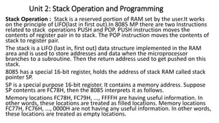
  • 1. Stack Operation : Stack is a reserved portion of RAM set by the user.It works on the principle of LIFO(last in first out).In 8085 MP there are two Instructions related to stack operations PUSH and POP. PUSH instruction moves the contents of register pair in to stack. The POP instruction moves the contents of stack to register pair. The stack is a LIFO (last in, first out) data structure implemented in the RAM area and is used to store addresses and data when the microprocessor branches to a subroutine. Then the return address used to get pushed on this stack. 8085 has a special 16-bit register, holds the address of stack RAM called stack pointer SP. SP is a special purpose 16-bit register. It contains a memory address. Suppose SP contents are FC78H, then the 8085 interprets it as follows. Memory locations FC78H, FC79H, ..., FFFFH are having useful information. In other words, these locations are treated as filled locations. Memory locations FC77H, FC76H, ..., 0000H are not having any useful information. In other words, these locations are treated as empty locations. Unit 2: Stack Operation and Programming
  • 2. • On a stack, we can perform two operations. PUSH and POP. In case of PUSH operation, the SP register gets decreased by 2 and new data item used to insert on to the top of the stack. On the other hand, in case of POP operation, the data item will have to be deleted from the top of the stack and the SP register will get increased by the value of 2. • Thus, the contents of SP specify the top most useful location in the stack. In other words, it indicates the memory location with the smallest address having useful information. Fig. Interpretation of SP contents
  • 3. Read and Write the stack in 8085 Microprocessor • Reading from the Stack • Let us consider that SP contents the address FC78H, and we want to read information from a stack location. In this case, we are not interested in reading from a location whose address is less than the memory address present in SP. This is because 8085 interprets them as useless information. For example, there is no point in reading useless information from memory location FC75H. • SP interprets that, memory locations FC78H, FC79H, ..., FFFFH are all interpreted by 8085 to have useful information. To read from Stack, the instruction is POP in 8085 microprocessor instruction set. Here we shall discuss more about the POP instruction below. • In 8085 Instruction set, with the mnemonic POP, we can pop out 2-Bytes from the top of the stack through rp i.e. register pair e.g. BC, DE, HL or AF. Here AF is a register pair formed with Flag and Accumulator registers and also known as PSW (Processor Status Word). In PSW, Accumulator is the MS Byte, and Flags register is the LS Byte.
  • 4. Mnemonics, Operand Opcode (in HEX) Bytes POP B C1 1 POP D D1 1 POP H E1 1 POP PSW F1 1
  • 5. rp Code Register Pair 0 0 BC 0 1 DE 1 0 HL 1 1 SP or PSW, but never both at the same time.
  • 6. • Let us consider the following example for a better understanding of the operation of the instruction.Here we are considering the instruction POP D which is an instruction falling in the category. As rp can have any of the four values, there are four opcodes for this type of instruction. It occupies only 1-Byte in memory. POP D is an example of instruction of this type. It is 1-Byte instruction. The result of the execution of this instruction is shown below with an example. Before After (BC) AABBH AABBH (SP) 3FFEH 4000H (3FFFH) AAH AAH (3FFEH) BBH BBH (DE) Any value AABBH
  • 7. Address Hex Codes Mnemonic Comment 2000 01 LXI B, AABBH Initializing BC register pair with AABBH 2001 BB Low order Byte BBH 2002 AA High order Byte AAH 2003 31 LXI SP,4000H Initializing SP with 4000H 2004 00 Low order Byte 00H 2005 40 High order Byte 40H 2006 C5 PUSH B At 3FFFH, AAH and at 3FFEH, BBH will be moved 2007 D1 POP D Popping and initializing DE register pair with stack contents The timing diagram against this instruction POP D execution is as follows –
  • 8. • Writing to the Stack • Let us consider that SP contents are FC7AH, and we want to write information to a stack location. In this case, we are not interested in writing to a location whose address is equal or greater than the memory address present in SP. This is because the 8085 interprets them as having useful information, which should not be destroyed! For example, there is no point in overwriting and destroying useful information at memory location FD7AH. We should be writing into a location where there is presently useless information, and make it useful. • To write onto Stack, the instruction is PUSH in 8085 microprocessor instruction set. Here we shall discuss more about the PUSH instruction below. • In 8085 Instruction set, PUSH rp instruction stores contents of register pair rp by pushing it into two locations above the top of the stack. rp stands for one of the following register pairs. • rp = BC, DE, HL, or PSW • As rp can have any of the four values, there are four opcodes for this type of instruction. It occupies only 1-Byte in memory. Note : POP requires 1-Byte, 3-Machine Cycles (Opcode Fetch, Memory Read, Memory Read) and 10 T-States for execution.
  • 9. Mnemonics, Operand Opcode (in HEX) Bytes PUSH B C5 1 PUSH D D5 1 PUSH H E5 1 PUSH PSW F5 1 In the above mention Opcodes, 2-bits are occupied to mention the register pair. 2-bits can have 4 combinations. So 4 register pairs can be mentioned with POP. As mentioned earlier, they are BC, DE, HL, and AF or PSW. Note with LXI instruction, we are having 4 possible register pairs can be used i.e. BC, DE, HL, and SP. So at the same time, we can’t have SP and PSW applicable with the same instruction.
  • 10. rp Code Register Pair 0 0 BC 0 1 DE 1 0 HL 1 1 SP or PSW, but never both at the same time. Let us consider PUSH B as an example of instruction of this category. It is 1-Byte instruction. The result of the execution of this instruction is shown below with an example.
  • 11. Before After (BC) AABBH AABBH (SP) 4000H 3FFEH (3FFFH) Any value AAH (3FFEH) Any value BBH
  • 12. Address Hex Codes Mnemonic Comment 2000 01 LXI B, AABBH Initializing BC register pair with AABBH 2001 BB Low order Byte BBH 2002 AA High order Byte AAH 2003 31 LXI SP,4000H Initializing SP with 4000H 2004 00 Low order Byte 00H 2005 40 High order Byte 40H 2006 C5 PUSH B At 3FFFH, AAH and at 3FFEH, BBH will be moved Note : PUSH B requires 1-Byte, 3-Machine Cycles (Opcode Fetch-1MC, Memory Write-2 MC) and 12 T-States for execution.
  • 13. SUBROUTINES: • a subroutine is a sequence of program instructions that perform a specific task, packaged as a unit. This unit can then be used in programs wherever that particular task have to be performed. A subroutine is often coded so that it can be started (called) several times and from several places during one execution of the program, including from other subroutines, and then branch back (return) to the next instruction after the call, once the subroutine’s task is done. It is implemented by using Call and Return instructions. The different types of subroutine instructions are • Unconditional Call instruction – CALL address is the format for unconditional call instruction. After execution of this instruction program control is transferred to a sub-routine whose starting address is specified in the instruction. Value of PC (Program Counter) is transferred to the memory stack and value of SP (Stack Pointer) is decremented by 2.
  • 14. Conditional Call instruction – In these instructions program control is transferred to subroutine and value of PC is pushed into stack only if condition is satisfied. INSTRUCTION PARAMETER COMMENT CC 16-bit address Call at address if cy (carry flag) = 1 CNC 16-bit address Call at address if cy (carry flag) = 0 CZ 16-bit address Call at address if ZF (zero flag) = 1 CNZ 16-bit address Call at address if ZF (zero flag) = 0 CPE 16-bit address Call at address if PF (parity flag) = 1 CPO 16-bit address Call at address if PF (parity flag) = 0 CN 16-bit address Call at address if SF (signed flag) = 1 CP 16-bit address Call at address if SF (signed flag) = 0
  • 15. • Unconditional Return instruction – RET is the instruction used to mark the end of sub-routine. It has no parameter. After execution of this instruction program control is transferred back to main program from where it had stopped. Value of PC (Program Counter) is retrieved from the memory stack and value of SP (Stack Pointer) is incremented by 2. • Conditional Return instruction – By these instructions program control is transferred back to main program and value of PC is popped from stack only if condition is satisfied. There is no parameter for return instruction.
  • 16. INSTRUCTION COMMENT RC Return from subroutine if cy (carry flag) = 1 RNC Return from subroutine if cy (carry flag) = 0 RZ Return from subroutine if ZF (zero flag) = 1 RNZ Return from subroutine if ZF (zero flag) = 0 RPE Return from subroutine if PF (parity flag) = 1 RPO Return from subroutine if PF (parity flag) = 0 RN Return from subroutine if SF (signed flag) = 1 RP Return from subroutine if SF (signed flag) = 0
  • 17. • Advantages of Subroutine – • Decomposing a complex programming task into simpler steps. • Reducing duplicate code within a program. • Enabling reuse of code across multiple programs. • Improving tractability or makes debugging of a program easy.
  • 18.
  • 19.
  • 20.
  • 21.
  • 22.
  • 23.
  • 24.
  • 25. LABEL OPCODE OPERAND COMMENTS T STATES MVI C , FFH ; Load register C 7 Loop : DCR C ; Decrement C 4 JNZ LOOP ; Jump back to 10/7 decrement C Clock frequency of the system = 2 MHz Clock period= 1/T= 0.5 μs Time to execute MVI = 7 T states * 0.5= 3.5 μs Time Delay in Loop TL= T*Loop T states * N10 = 0.5 * 14* 255 = 1785 μs = 1.8 ms N10 = Equivalent decimal number of hexadecimal count loaded in the delay register TLA= Time to execute loop instructions =TL –(3T states* clock period)=1785-1.5=1783.5 μs
  • 26.
  • 27. TIME DELAY USING A REGISTER PAIR : Label Opcode Operand Comments T states LXI B , 2384H Load BC with 16-bit count 10 LOOP : DCX B Decrement BC by 1 6 MOV A,C Place contents of C in A 4 ORA B OR B with C to set Zero flag 4 JNZ LOOP if result not equal to 0 , 10/7 jump back to loop Time Delay in Loop TL= T*Loop T states * N10 = 0.5 * 24* 9092 = 109 ms Time Delay using a LOOP within a LOOP : MVI B , 38H 7T LOOP2: MVI C , FFH 7T LOOP1: DCR C 4T JNZ LOOP1 10/7 T DCR B 4T JNZ LOOP 2 10/7T Delay in Loop TL1=1783.5 μs , Delay in Loop TL2= (0.5*21+TL1)*56 =100.46ms .
  • 28. ILLUSTRATIVE PROGRAM: HEXADECIMAL COUNTER Write a Program to count continuously from FFH to 00H using register C with delay count 8CH between each count and display the number at one of the output ports. MVI B,00H NEXT: DCR B MVI C,8CH DELAY: DCR C JNZ DELAY MOV A,B OUT PORT# JMP NEXT
  • 29. ILLUSTRATIVE PROGRAM: ZERO TO NINE (MODULO TEN) COUNTER START: MVI B,00H MOV A,B DSPLAY: OUT PORT # LXI H,16-bit LOOP: DCX H MOV A,L ORA H JNZ LOOP INR B MOV A,B CPI 0AH JNZ DSPLAY JZ START Flow Chart: Start Initialize counter Display Output Load Delay register Decrement Delay register Is Delay register=0? Next Count Is count =0AH? If yes, Initialize counter If no, Display Output
  • 30. Timing Diagram: Timing Diagram is a graphical representation. It represents the execution time taken by each instruction in a graphical format. The execution time is represented in T- sates.It represents the clock cycle and duration, delay, content of address bus and data bus, type of operation I e. Read/write/status signals. Machine Cycle:The time required to access the memory or input/output devices is called machine cycle. T-State: Instruction Cycle: The time required to execute an instruction is called instruction cycle. The machine cycle and instruction cycle takes multiple clock periods. A portion of an operation carried out in one system clock period is called as T-state.
  • 31. Machine cycles of 8085 The 8085 microprocessor has 5 (seven) basic machine cycles. They are  Opcode fetch cycle (4T)  Memory read cycle (3 T)  Memory write cycle (3 T)  I/O read cycle (3 T)  I/O write cycle (3 T)
  • 32. Signal 1.Opcode fetch machine cycle of 8085 :
  • 33. Each instruction of the processor has one byte opcode.  The opcodes are stored in memory. So, the processor executes the opcode fetch machine cycle to fetch the opcode from memory.  Hence, every instruction starts with opcode fetch machine cycle.  The time taken by the processor to execute the opcode fetch cycle is 4T.  In this time, the first, 3 T-states are used for fetching the opcode from memory and the remaining T-states are used for internal operations by the processor.
  • 34. 2. Memory Read Machine Cycle of 8085:  The memory read machine cycle is executed by the processor to read a data byte from memory.  The processor takes 3T states to execute this cycle. The instructions which have more than one byte word size will use the machine cycle after the opcode fetch machine cycle.
  • 35.
  • 36. Cycle 3. Memory Write Machine Cycle of 8085
  • 37. The memory write machine cycle is executed by the processor to write a data byte in a memory location.  The processor takes, 3T states to execute this machine cycle. 4. I/O Read Cycle of 8085  The I/O Read cycle is executed by the processor to read a data byte from I/O port or from the peripheral, which is I/O, mapped in the system.  The processor takes 3T states to execute this machine cycle.  The IN instruction uses this machine cycle during the execution.
  • 38.
  • 40. Operation: •It is used to writ one byte into IO device. •It requires 3 T-States. •During T1, the lower byte of address is duplicated into higher order address bus A8-A15. •ALE is high and A0-A7 address is selected from AD0-AD7. •As it is an IO operation IO/M (bar) goes low. •During T2, ALE goes low, WR (bar) goes low and data appears on AD0-AD7 to write data into IO device. •During T3, Data remains on AD0-AD7 till WR(bar) is low.
  • 41. Examples:1. Timing diagram for STA 526AH
  • 42. STA means Store Accumulator -The contents of the accumulator is stored in the specified address (526A H). The opcode of the STA instruction is said to be 32H. It is fetched from the memory 41FFH (see fig). - OF machine cycle Then the lower order memory address is read (6AH). - Memory Read Machine Cycle Read the higher order memory address (52H).- Memory Read Machine Cycle The combination of both the addresses are considered and the content from accumulator is written in 526AH. - Memory Write Machine Cycle Assume the memory address for the instruction and let the content of accumulator is C7H. So, C7H from accumulator is now stored in 526AH.
  • 43. 2.Timing diagram for INR M: Fetching the Opcode 34H from the memory 4105H. (OF cycle).Let the memory address (M) be 4250H. (MR cycle - To read Memory address and data).Let the content of that memory is 12H.Increment the memory content from 12H to 13H. (MW machine cycle)
  • 44.
  • 45. MP 8085 Assembly Language Programming: 1. Store 8-bit data in memory using direct addressing: • MVI A, 49H : "Store 49H in the accumulator" • STA 2501H : "Copy accumulator contents at address 2501H" • HLT : "Stop" 2. Store 8-bit data in memory using indirect addressing: • LXI H : "Load H-L pair with 2501H" • MVI M : "Store 49H in memory location pointed by H- L register pair (2501H)" • HLT : "Stop"
  • 46. 3. Data Transfer and memory operations (Direct and Indirect Addressing): To write an Assembly Language Program to transfer a data block without overlap using 8085 ALGORITHM: STEP 1: Load the DE pair with the destination address. STEP 2: Load the HL pair with the count of elements in the data block. STEP 3: Load element in the data block. STEP 4: Increment the source address. STEP 5: Copy the element to the accumulator and then transfer it to the destination address. STEP 6: Increment destination address. STEP 7: Decrement the count. STEP 8: If Count = 0 then go to the next step else go to step 3. STEP 9: Terminate the program.
  • 48. ALP : SOURCE CODE : LABEL : MNEMONIC COMMENT LXI D,4500 Load destination address in DE pair LXI H,4100 Load the count in HL pair MOV C,M Copy the count to register C LOOP: INX H Increment memory MOV A,M Copy element to Accumulator STAX D Store the element to the address in the DE pair INX D Increment destination address DCR C Decrement count JNZ LOOP Jump on non-zero to the label LOOP HLT Program ends
  • 49. Address Hex Codes Label Mnemonic T-States Comment 8000 11,50,80 START: LXI D, 8050H 10 Setup HL pair as a pointer for source memory. 8003 21,70,80 LXI H, 8070H 10 Set up DE pair as a pointer for destination memory 8006 4E MOV C , M 7 Set up B to count 16 bytes 8008 23 LOOP: INX H 7 Get data byte from source. 8009 7E MOV A,M 7 Store data byte as destination 800A 12 STAX D 6 Point HL to next source location 800B 13 INX D 6 Point DE to next destination 800C 0D DCR C 4 Decrement count 800D C2,08,80 JNZ LOOP 10 If counter is not 0, go back to transfer next byte. 8010 76 HLT 5 Stop
  • 50. 4. Add two 8-bit numbers: Example (2501 H) = 99H (2502 H) = 39H Result (2503 H) = 99H + 39H = D2H Since, 1 0 0 1 1 0 0 1 (99H) + 0 0 1 1 1 0 0 1 (39H) 1 1 0 1 0 0 1 0 (D2H) Program 1.LXI H, 2501H : "Get address of first number in HL pair. Now H-L points to 2501H" 2.MOV A, M : "Get first operand in accumulator" 3.INX H : "Increment content of HL pair. Now, HL points 2502H" 4.ADD M : "Add first and second operand" 5.INX H : "H-L points 4002H" 6.MOV M, A : "Store result at 2503H" 7.HLT : "Stop"
  • 51. Subtract two 8-bit numbers: Example (2501 H) = 49H (2502 H) = 32H Result (2503 H) = 49H - 32H = 17H Program 1.LXI H, 2501H : "Get address of first number in HL pair. Now H-L points to 2501H" 2.MOV A, M : "Get first operand in accumulator" 3.INX H : "Increment content of HL pair. Now, HL points 2502H" 4.SUB M : "Subtract first to second operand" 5.INX H : "H-L points 4002H" 6.MOV M, A : "Store result at 2503H" 7.HLT : "Stop"
  • 52. 5.Add two 16-bits numbers: Add the 16-bit number in memory locations 2501H and 2502H to the 16-bit number in memory locations 2503H and 2504H. The most significant eight bits of the two numbers to be added are in memory locations 2502H and 4004H. Store the result in memory locations 2505H and 2506H with the most significant byte in memory location 2506H. Example (2501H) = 15H (2502H) = 1CH (2503H) = B7H (2504H) = 5AH Result = 1C15 + 5AB7H = 76CCH (2505H) = CCH (2506H) = 76H
  • 53. . Program : • Add two 16-bits number with ADD and ADC instruction • LHLD 2501H : "Get 1st 16-bit number in H-L pair" • XCHG : "Save 1st 16-bit number in DE" • LHLD 2503H : "Get 2nd 16-bit number in H-L pair" • MOV A, E : "Get lower byte of the 1st number" • ADD L : "Add lower byte of the 2nd number" • MOV L, A : "Store result in L-register" • MOV A, D : "Get higher byte of the 1st number" • ADC H : "Add higher byte of the 2nd number with CARRY" • MOV H, A : "Store result in H-register" • SHLD 4004H : "Store 16-bit result in memory locations 2505H and 2506H" • HLT : "Stop"
  • 54. Add two 16-bits numbers with DAD instruction : • LHLD 2501H : "Get 1st 16-bit number" • XCHG : "Save 1st 16-bit number in DE" • LHLD 2503H : "Get 2nd 16-bit number in H-L" • DAD D : "Add DE and HL" • SHLD 2505H : "Store 16- bit result in memory locations 2505H and 2506H". • HLT : "Stop" Subtract two 16-bit numbers: Example (2500H) = 19H (2501H) = 6AH (2504H) = 15H (2503H) = 5CH Result = 6A19H ? 5C15H = OE04H (2504H) = 04H (2505H) = OEH
  • 55. • Program:16-Bits Substraction: • LHLD 2500H : "Get first 16-bit number in HL" • XCHG : "Save first 16-bit number in DE" • LHLD 2502H : "Get second 16-bit number in HL" • MOV A, E : "Get lower byte of the first number" • SUB L : "Subtract lower byte of the second number" • MOV L, A : "Store the result in L register" • MOV A, D : "Get higher byte of the first number" • SBB H : "Subtract higher byte of second number with borrow" • MOV H, A : "Store l6-bit result in memory locations 2504H and 2505H" • SHLD 2504H : "Store l6-bit result in memory locations 2504H and 2505H" • HLT : "Terminate program execution"
  • 56. ADD CONTENTS OF TWO MEMORY LOCATIONS: Example (2500H) = 7FH (2501H) = 89H Result = (2502H) = 08H (2503H) = 01H Program 1.LXI H, 2500H : "HL Points 2500H" 2.MOV A, M : "Get first operand" 3.INX H : "HL Points 2501H" 4.ADD M : "Add second operand" 5.INX H : "HL Points 2502H" 6.MOV M, A : "Store the lower byte of result at 2502H" 7.MVIA, 00 : "Initialize higher byte result with 00H" 8.ADC A : "Add carry in the high byte result" 9.INX H : "HL Points 2503H" 10.MOV M, A : "Store the higher byte of result at 2503H" 11.HLT : "Terminate program execution"
  • 57. To perform the multiplication of two 8 bit numbers using 8085: ALGORITHM 1) Start the program by loading HL register pair with address of memory location. 2) Move the data to a register (B register). 3) Get the second data and load into Accumulator. 4) Add the two register contents. 5) Check for carry. 6) Increment the value of carry. 7) Check whether repeated addition is over and store the value of product and carry in memory location. 8) Terminate the program. SOURCE CODE MVI D, 00 Initialize register D to 00 MVI A, 00 Initialize Accumulator content to 00 LXI H, 4150
  • 58. MOV B, M Get the first number in B - reg INX H MOV C, M Get the second number in C- reg. LOOP: ADD B Add content of A - reg to register B. JNC NEXT Jump on no carry to NEXT. INR D Increment content of register D NEXT: DCR C Decrement content of register C. JNZ LOOP Jump on no zero to address STA 4152 Store the result in Memory MOV A, D Move the content of D register to Accumulator STA 4153 Store the MSB of result in Memory HLT Terminate the program. Input : FF (4150) FF (4151) Output: 01 (4152) FE (4153)
  • 59. To perform the division of two 8 bit numbers using 8085: ALGORITHM : 1) Start the program by loading HL register pair with address of memory location. 2) Move the data to a register (B register). 3) Get the second data and load into Accumulator. 4) Compare the two numbers to check for carry. 5) Subtract the two numbers. 6) Increment the value of carry. 7) Check whether repeated subtraction is over and store the value of product and carry in memory location. 8) Terminate the program. SOURCE CODE: LXI H, 4150 MOV B, M Get the dividend in B – reg. MVI C, 00 Clear C – reg for quotient
  • 60. INX H MOV A, M Get the divisor in A – reg. NEXT: CMP B Compare A - reg with register B. JC LOOP Jump on carry to LOOP SUB B Subtract A – reg from B- reg. INR C Increment content of register C. JMP NEXT Jump to NEXT LOOP: STA 4152 Store the remainder in Memory MOV A, C Move the Content of C register to Accumulator STA 4153 Store the quotient in memory HLT Terminate the program. Input: FF (4150) FF (4251) Output: 01 (4152) - Remainder FE (4153) - Quotient RESULT Thus the program to divide two 8-bit numbers was executed.
  • 61. To find the largest number in an array of data using 8085 instruction set: ALGORITHM STEP 1: Load the address of the first element of the array in HL pair STEP 2: Move the count to B – reg. STEP 3: Increment the pointer STEP 4: Get the first data in A – reg. STEP 5: Decrement the count. STEP 6: Increment the pointer STEP 7: Compare the content of memory addressed by HL pair with that of A - reg. STEP 8: If Carry = 0, go to step 10 or if Carry = 1 go to step 9 STEP 9: Move the content of memory addressed by HL to A – reg. STEP 10: Decrement the count STEP 11: Check for Zero of the count. If ZF = 0, go to step 6, or if ZF = 1 go to next step. STEP 12: Store the largest data in memory. STEP 13: Terminate the program.
  • 62. SOURCE CODE: LXI H,4200 Set pointer for array MOV B,M Load the Count INX H MOV A,M Set 1st element as largest data DCR B Decrement the count LOOP: INX H CMP M If A- reg > M go to AHEAD JNC AHEAD MOV A,M Set the new value as largest AHEAD: DCR B JNZ LOOP Repeat comparisons till count = 0 STA 4300 Store the largest value at 4300 HLT Input: 05 (4200) -- Array Size 0A (4201) F1 (4202) 1F (4203) 26 (4204) FE (4205) Output: FE (4300) RESULT Thus the program to find the largest number in an array of data was executed
  • 63. To find the smallest number in an array of data using 8085 instruction set: ALGORITHM: STEP 1: Load the address of the first element of the array in HL pair STEP 2: Move the count to B – reg. STEP 3: Increment the pointer STEP 4: Get the first data in A – reg. STEP 5: Decrement the count. STEP 6: Increment the pointer STEP 7: Compare the content of memory addressed by HL pair with that of A - reg. STEP 8: If carry = 1, go to step 10 or if Carry = 0 go to step 9 STEP 9: Move the content of memory addressed by HL to A – reg. STEP 10: Decrement the count STEP 11: Check for Zero of the count. If ZF = 0, go to step 6, or if ZF = 1 go to next step. STEP 12: Store the smallest data in memory. STEP 13: Terminate the program.
  • 64. SOURCE CODE : LXI H,4200 Set pointer for array MOV B,M Load the Count INX H MOV A,M Set 1st element as largest data DCR B Decrement the count LOOP: INX H CMP M If A- reg < M go to AHEAD JC AHEAD MOV A,M Set the new value as smallest AHEAD: DCR B JNZ LOOP Repeat comparisons till count = 0 STA 4300 Store the largest value at 4300 HLT Input: 05 (4200) - Array Size 0A (4201) F1 (4202) 1F (4203) 26 (4204) FE (4205) Output: 0A (4201) RESULT Thus the program to find the smallest number in an array of data was executed
  • 65. WRITE AN ALP TO SORT THE SERIES IN ASCENDING ORDER: Algorithm: 1.Initialize the source memory pointer. 2.Initialize two counters: one to compare the data and another to repeat the process of comparison till all the nos. are over. 3.The first and the next no. are compared. Smaller of the two is retained in the first memory location. The larger of the two is moved to the next memory location. 4.Decrement the count. 5.The second memory location is compared with the third and again step 3 is repeated till the count is zero. 6.At the end, the largest number will be at the last location. Data: N no. of bytes stored from 2201 onwards. Result: Numbers stored from 2201 are arranged in ascending order. Sample: N=(2200), source location: 2201 to 2205, destination location: 2201 to 2205
  • 66. Memory Addr. Opcode/ data Label Mnemonics Comments 7000,01,02 3A,00,22 LDA 2200H Load Acc with the count 7003 47 MOV B, A Save count to reg B. 7004,05,06 21,01,22 LOOP2 LXI H, 2201H Initialize HL pair with source memory. 7007 48 MOV C, B Initialize C with count 7008 7E LOOP1 MOV A, M Transfer src data to reg.A. 7009 23 INX H Increment HLpair by 1 700A BE CMP M Compare the two nos. 700B,0C,0D DA,13,70 JC DOWN If no.1<no.2,go to Label DOWN 700E 56 MOV D,M Save smaller no. in D 700F 77 MOV M,A Larger no. in II memory location.
  • 67. Memory Addr. Opcode/ data Label Mnemonics Comments 7010 2B DCX H Decrement HL 7011 72 MOVM,D Save smaller no. in I memory location. 7012 23 INX H Increment HL to point to next memory location. 7013 0D DOWN DCR C Decrement count by 7014,15,16 C2,08,70 JNZ LOOP1 If not zero, jump to loop1 7017 05 DCR B Decrement count by1 7018,19,1A C2,04,70 JNZ LOOP2 If not zero, jump to loop2 701B CF RST1 Stop Conclusion: Thus, program written for arranging numbers in ascending order is successfully executed.
  • 68. Program to arrange an array of data in descending order using 8085. Algorithm : 1) Initialize HL pair as memory pointer. 2) Get the count at 4200 in to C register. 3) Copy it in D register. 4) Get the first vale in Accumulator. 5) Compare it with the value at next location. 6) If they are out of order, exchange the contents of accumulator and memory. 7) Decrement D register’s content by 1. 8) Repeat steps 5 and 7 till the value in D register become zero. 9) Decrement C register’s content by 1. 10) Repeat steps 3 to 9 till the value in C register becomes zero. 11) Terminate the program.
  • 69. Program : MEMORY LABEL MNEMONIC HEX CODE COMMENT 4400 LXI H,4200 21,00,42 Load the array size to the HL pair 4403 MOV C,M 4E Copy the array size to C register 4404 DCR C 0D Decrement C by 1 4405 REPEAT MOV D,C 51 Copy content of C to D register 4406 LXI H,4201 21,01,42 Load the first data to the HL pair 4409 LOOP MOV A,M 7E Copy the data to the accumulator 440A INX H 23 Increment memory by 1 440B CMP M BE Compare accumulator and memory content 440C JNC SKIP D2,14,44 Jump on no carry to the label SKIP 440F MOV B,M 46 Copy memory content to B register 4410 MOV M,A 77 Copy accumulator content to memory 4411 DCX H 2B Decrement memory by 1
  • 70. MEMORY LABEL MNEMONIC HEX CODE COMMENT 4412 MOV M,B 70 Copy B register’s content to memory 4413 INX H 23 Increment memory by 1 4414 SKIP DCR D 15 Decrement D by 1 4415 JNZ LOOP C2,09,44 Jump on non-zero to the label LOOP 4418 DCR C 0D Decrement C by 1 4419 JNZ REPEAT C2,05,44 Jump on non-zero to the label REPEAT 441C HLT 76 Program ends Input at 4200 : 05H (Array Size) 4201 : 01H 4202 : 02H 4203 : 03H 4204 : 04H 4205 : 05H Output at 4200 : 05H (Array Size) 4201 : 05H 4202 : 04H 4203 : 03H 4204 : 02H 4205 : 01H
  • 71. Program to Add two multi-byte numbers in 8085 Microprocessor We are using 4-byte numbers. The numbers are stored into the memory at location 8501H and 8505H. One additional information is stored at location 8500H. In this place we are storing the byte count. The result is stored at location 85F0H. The HL pair is storing the address of first operand bytes, the DE is storing the address of second operand bytes. C is holding the byte count. We are using stack to store the intermediate bytes of the result. After completion of the addition operation, we are popping from the stack and storing into the destination. Input: 8500H = 04H=Byte Count. First number in memory loc :8501H=19H , 8502H=68H , 8503H=12H , 8504H=85. Second number in memory loc:8505H=88H,8506H=25H,8507H=17H,8508H=20H.
  • 72. Flow Diagram: Multi Byte Addition
  • 73. Program: Address HEX Codes Labels Mnemonics Comments F000 31, 00, 20 LXI SP,2000H Initialize Stack Pointer F003 21, 00, 85 LXI H,8500H load memory address to get byte count F006 4E MOV C,M load memory content into C register F007 06, 00 MVI B,00H clear B register F009 21, 01, 85 LXI H, 8501H load first argument address F00C 11, 05, 85 LXI D, 8505H load second argument address
  • 74. Address HEX Codes Labels Mnemonics Comments F00F 1A LOOP LDAX D load DE with second operand address F010 8E ADC M Add memory content and carry with Acc F011 F5 PUSH PSW Store the accumulator content into stack F012 04 INR B increase b after pushing into stack F013 23 INX H Increase HL pair to point next address F014 13 INX D Increase DE pair to point next address F015 0D DCR C Decrease c to while all bytes are not exhausted
  • 75. Address HEX Codes Labels Mnemonics Comments F016 C2, 0F, F0 JNZ LOOP When bytes are not considered, loop again F019 D2, 20, F0 JNC SKIP when carry = 0, jump to store F01C 3E, 01 MVI A,01H when carry = 1, push it into stack F01E F5 PUSH PSW Store the accumulator content into stack F01F 04 INR B increase b after pushing into stack F020 21, F0, 85 SKIP LXI H,85F0H load the destination pointer F023 F1 L1 POP PSW pop AF to get back bytes from stack
  • 76. Address HEX Codes Labels Mnemonics Comments F024 77 MOV M,A store Acc data at memory location pointed by HL F025 23 INX H Increase HL pair to point next address F026 05 DCR B Decrease B F027 C2, 23, F0 JNZ L1 Go to L1 to store stack contents F02A 76 HLT Terminate the program Output Output : 85F0=00 , 85F1=A5 , 85F2=29 , 85F3=8D , 85F4=A1
  • 77. program to find 1’s and 2’s complement of 8-bit number: MEMORY MNEMONICS OPERANDS COMMENT 2000 LDA [3000] [A] <- [3000] 2003 CMA [A] <- [A^] 2004 STA [3001] 1’s complement 2007 ADI 01 [A] <- [A] + 01 2009 STA [3002] 2’s complement 200C HLT Stop Algorithm – 1.Load the data from memory 3000 into A (accumulator) 2.Complement content of accumulator 3.Store content of accumulator in memory 3001 (1’s complement) 4.Add 01 to Accumulator content 5.Store content of accumulator in memory 3002 (2’s complement) 6.Stop Program –
  • 78. program to find the factorial of a number: Algorithm – 1.Load the data into register B 2.To start multiplication set D to 01H 3.Jump to step 7 4.Decrements B to multiply previous number 5.Jump to step 3 till value of B>0 6.Take memory pointer to next location and store result 7.Load E with contents of B and clear accumulator 8.Repeatedly add contents of D to accumulator E times 9.Store accumulator content to D 10.Go to step 4 Explanation – 1.First set register B with data. 2.Set register D with data by calling MULTIPLY subroutine one time. 3.Decrement B and add D to itself B times by calling MULTIPLY subroutine as 4*3 is equivalent to 4+4+4 (i.e., 3 times). 4.Repeat the above step till B reaches 0 and then exit the program. 5.The result is obtained in D register which is stored in memory
  • 79. ADDRESS LABEL MNEMONIC COMMENT 2000H Data Data Byte 2001H Result Result of factorial 2002H LXI H, 2000H Load data from memory 2005H MOV B, M Load data to B register 2006H MVI D, 01H Set D register with 1 2008H FACTORIAL CALL MULTIPLY Subroutine call for multiplication 200BH DCR B Decrement B 200CH JNZ FACTORIAL Call factorial till B becomes 0 200FH INX H Increment memory 2010H MOV M, D Store result in memory
  • 80. ADDRESS LABEL MNEMONIC COMMENT 2011H HLT Halt 2100H MULTIPLY MOV E, B Transfer contents of B to C 2101H MVI A, 00H Clear accumulator to store result 2103H MULTIPLYLOOP ADD D Add contents of D to A 2104H DCR E Decrement E 2105H JNZ MULTIPLYLOOP Repeated addition 2108H MOV D, A Transfer contents of A to D 2109H RET Return from subroutine
  • 81. Example – Assume Fibonacci series is stored at starting memory location 3050. Note – This program generates Fibonacci series in hexadecimal numbers. 8085 program to generate Fibonacci series
  • 82. Algorithm – For Fibonacci Series 1.Initialize register H with 30 and register L with 50, so that indirect memory M points to memory location 3050. 2.Initialize register B with 00, register C with 08 and register D with 01. 3.Move the content of B in M. 4.Increment M by 1 so that M points to next memory location. 5.Move the content of D in M. 6.Move the content of B in accumulator A. 7.Add the content of D in A. 8.Move the content of D in B. 9.Move the content of A in D. 10.Increment M by 1 so that M points to next memory location. 11.Move the content of A in M. 12.Decrements C by 1. 13.Jump to memory location 200C if ZF = 0 otherwise Halt the program.
  • 83. Program – For Fibonacci Series: MEMORY ADDRESS MNEMONICS COMMENT 2000 LXI H, 3050 H <- 30, L <- 50 2003 MVI C, 08 C <- 08 2005 MVI B, 00 B <- 00 2007 MVI D, 01 D <- 01 2009 MOV M, B M <- B 200A INX H M <- M + 01 200B MOV M, D M <- D 200C MOV A, B A <- B
  • 84. MEMORY ADDRESS MNEMONICS COMMENT 200D ADD D A <- A + D 200E MOV B, D B <- D 200F MOV D, A D <- A 2010 INX H M <- M + 01 2011 MOV M, A M <- A 2012 DCR C C <- C – 01 2013 JNZ 200C Jump if ZF = 0 2016 HLT END
  • 85. find 1’s and 2’s complement of 16-bit number: Algorithm – 1.Load a 16-bit number from memory 3000 into a register pair (H-L) 2.Move content of register L to accumulator 3.Complement content of accumulator 4.Move content of accumulator to register L 5.Move content of register H to accumulator 6.Complement content of accumulator 7.Move content of accumulator to register H 8.Store content of register pair in memory 3002 (1’s complement) 9.Increment content of register pair by 1 10.Store content of register pair in memory 3004 (2’s complement) 11.Stop
  • 86. MEMORY MNEMONICS OPERANDS COMMENT 2000 LHLD [3000] [H-L] <- [3000] 2003 MOV A, L [A] <- [L] 2004 CMA [A] <- [A^] 2005 MOV L, A [L] <- [A] 2006 MOV A, H [A] <- [H] 2007 CMA [A] <- [A^] 2008 MOV H, A [H] <- [A] 2009 SHLD [3002] 1’s complement 200C INX H [H-L] <- [H-L] + 1 200D SHLD [3004] 2’s complement 2010 HLT Stop Program – 1s and 2s Comlement of 16- bits Number:
  • 87. Program for Number of 1s and 0s in a Byte: Write a program to count number of ones in the given 8-bit number use register B to display the count of ones where starting address is 2000 and the number is stored at 3000 memory address and store result into 3001 memory address. Example:
  • 88. Algorithm – 1.Move 00 to register B immediately for count 2.Move 08 to register C immediately for shifting 3.Load the data of memory [3000] into accumulator 4.Rotate ‘A’ right with carry 5.Jump if no carry to step-7 6.Otherwise increase register B by 1 7.Decrease register C by 1 8.Jump if not zero to step-4 9.Move content of register B into accumulator 10.Store content of accumulator into memory [3001] (number of count) 11.Stop
  • 89. Program –To count number of 1s and zeros in a byte: MEMORY MNEMONICS OPERANDS COMMENT 2000 MVI B, 00 [B] <- 00 2002 MVI C, 08 [C] <- 08 2004 LDA [3000] [A] <- [3000] 2007 RAR rotate ‘A’ right with carry 2008 JNC 200C jump if no carry 200B INR B [B] <- [B] + 1 200C DCR C [C] <- [C] – 1 200D JNZ 2007 jump if not zero 2010 MOV A, B [A] <- [B] 2011 STA [3001] number of ones 2014 2016 2017 201A MVI SUB STA HLT A,08 B [3002] [C]=[08] [A]=[08]-[B] Number of zeros Stop
  • 90. Explanation – Registers A, B and C are used for general purpose. 1.MVI is used to load an 8-bit given register immediately (2 Byte instruction) 2.LDA is used to load accumulator direct using 16-bit address (3 Byte instruction) 3.MOV is used to transfer the data from accumulator to register(any) or register(any) to accumulator (1 Byte) 4.RAR is used to shift ‘A’ right with carry (1 Byte instruction) 5.STA is used to store data from accumulator into memory direct using 16-bit address (3 Byte instruction) 6.INR is used to increase given register by 1 (1 Byte instruction) 7.JNC is used to jump to the given step if their is no carry (3 Byte instruction) 8.JNZ is used to jump to the given step if their is not zero (3 Byte instruction) 9.DCR is used to decrease given register by 1 (1 Byte instruction) 10.HLT is used to halt the program