The hardware of the Mcs 51 microcontroller
•Download as PPT, PDF•
0 likes•184 views

This is the second chapter of the one behind make sure you download it bit by bit to have a more meaningful understanding

Recommended
More Related Content
What's hot
What's hot (20)
Similar to The hardware of the Mcs 51 microcontroller
Similar to The hardware of the Mcs 51 microcontroller (20)
Recently uploaded
Recently uploaded (20)
The hardware of the Mcs 51 microcontroller
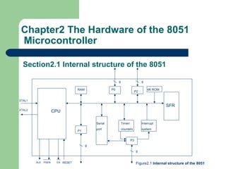
- 1. Chapter2 The Hardware of the 8051 Microcontroller Section2.1 Internal structure of the 8051 CPU RAM 4K ROMP0 P2 P1 P3 Serial port Timer/ counters Interrupt system SFR ALE XTAL1 XTAL2 8 8 8 8 PSEN RESETEA Figure2.1 Internal structure of the 8051
- 2. The important features,most of which are common to all microcontrollers,are: 1.CPU:Central Processing Unit Playing the role as a brain and heart of computer(including normal and special purpose computers),having very strong and multidimensional functions surrounding the mathematical and logical operation,but less independency and connection ability unless getting in a combination consisting of a lot of assistant elements. 2.Internal RAM RAM:Random Access Memory Up to 128/256 bytes or more data memory on chip for different chips -51 sub-serial 128 bytes (They are located from 00H to 7FH.) -52 sub-serial 256 bytes
- 3. 3. Internal ROM ROM:Read Only Memory Up to 4KB/ 8KB/16KB/32KB/64KB 8031: no 8051:4K(They are located from 0000H to 0FFFH.) 8751:4K EPROM(electrically programmable ROM) 4.I/O port There are four I/O ports named as P0, P1, P2 and P3 respectively. And there are thirty-two I/O pins arranged as four 8-bit ports. 5.Full Duplex UART Serial Port UART:Universal Asynchronous Receiver/Transmitter
- 4. 6. Two or three 16-bit timer/counters for different subserials -51 sub-serial two -52 sub-serial three As timers its pulse source is internal machine cycle. As counters its pulse source from I/O pins(P3.4 and P3.5). (P3.4 is the input of counter 0 and P3.5 is the input of counter 1.) 7.Five or six interrupt sources with 2 priority levels -51 sub-serial five -52 sub-serial six a five vector 2-level interrupt architecture
- 5. 8.SFR(21):Special Function Registers Including a mix of operational registers,I/O registers and control registers. They are located from 80H to FFH.
- 6. Section2.2 Pin connections and functions Figure 2.2 The pinout of the 8051 family The 8051 is available in several types of package to suit a variety of conditions and layout designs.Figure 2.2 shows the pinout for the popular 40-pin DIP package with the abbreviated names of the signals for each pin. It is important to note that many of the pins are used for more than one function,the alternate functions being shown in slash( 斜线 ).Because of this,not all of the possible 8051 features may be used at the same time.Programming instructions or physical pin connections determine the use of any muti-function pins.
- 7. For example,port 3 bit 0(abbreviated P3.0) may be used as a general purpose I/O pin,or as an input(RXD) to the serial port data receiver. The system designer decides which of these two functions is to be used,and designs the hardware and software affecting that pin accordingly.
- 8. There are 2 special power supply pins,2 external crystal pins,4 control pins and 32 I/O pins. 1.Main power supply pins Pin40:Vcc +5V Pin20:Vss ground connection 2.External crystal pins XTAL1:Input to the inverting oscillator amplifier and input to the internal clock operating circuit. XTAL2:output from the inverting oscillator amplifier. Oscillator characteristics: XTAL1 and XTAL2 are the input and output,respectively,of an inverting amplifier which can be configured for use as an on-chip oscillator,as shown in figure2.3.
- 9. C1,C2:30PF The range of the crystal oscillator frequency is usually from 1.2MHz to 12MHz. Either a quartz crystal or ceramic resonator may be used. Figure2.3 Internal Clock Drive Configuration 8051
- 10. Figure2.4 External Clock Drive Configuration To drive the device from an external clock source,XTAL2 should be left unconnected while XTAL1 is driven as shown in this figure. NC External oscillator signal
- 11. 3.Four control pins 1)pin9:RST(Reset input) A high level on this pin for two machine cycles while the oscillator is running resets the device. 2)pin30:ALE/ PROG Address Latch Enable output pulse for latching the low byte of the address during accesses to external memory. This pin is also the program pulse input( PROG) during EPROM programming. In normal operation ALE is emitted at a constant rate of 1/6 the oscillator frequency and may be used for external timing or clocking purposes.
- 12. 3)pin29:PSEN Program Strobe Enable is the read strobe( 闸门 ) to external program memory. When the 8051 is executing code from external program memory, PSEN is activated twice each machine cycle,except that (不同之处在 于) two PSEN activations are skipped during each access to external data memory. 4)pin31:EA/Vpp(External Access Enable/Voltage Pulse of Programming) EA must be strapped to GND in order to enable the device to fetch code from external program memory locations starting at 0000H to FFFFH.EA should be strpped to Vcc for internal program executions. This pin also receives the 21-volt programming enable voltage during EPROM programming ,for parts that require 21-volt Vpp.
- 13. 4.Thirty-two I/O pins: 1)pin39~pin32:P0.0~P0.7 or named as port 0,which is often used as multiplexed low order address/data bus during accesses to external program and data memory. P0 is often used as ADB. 2) pin1~pin8:P1.0~P1.7 or named as port 1,which is a true I/O port. 3) pin21~pin28:P2.0~P2.7 or named as port 2,which is often used to output the high order address when accessing external memory. 4) pin10~pin17:P3.0~P3.7 or named as port 3,which is often used as alternate functions.
- 14. All the pins on port 3 can be used for other purposes than simple input/output.Some are used for extended functions of the microcontroller,which others serve as inputs for particular operations.The functions are shown in Table 2.1. Port pin Alternate function Description P3.0 RXD Serial port input P3.1 TXD Serial port output P3.2 INT0 External Interrupt 0 P3.3 INT1 External Interrupt 1 P3.4 T0 Counter 0 external input P3.5 T1 Counter 1 external input P3.6 WR External data memory write strobe P3.7 RD External data memory read strobe
- 15. 5.Bus structure 1)AB:16-bit provided by P0 and P2 2)DB: 8-bit provided by P0 3)CB:P3 alternate functions RESET,ALE,PSEN,EA
- 16. Section2.3 Memory Organization in 8051 Microcontroller Physically the 8051 has four memory spaces. Internal/external program memory Internal/external data memory Logically it has three memory spaces,the whole program memory. FFFFH
- 17. 1.Program memory There are five special entrance units which are as following respectively. 0003H external interrupt 0 000BH timer 0 interrupt 0013H external interrupt 1 001BH timer 1 interrupt 0023H serial port interrupt
- 18. EA:strapped to Vss -----external program memory (64KB,0000H~FFFFH) strapped to Vcc -----internal program memory PC:0FFFH The address of internal and external program memory is continuous.
- 19. 2.External data memory It is possible to interface an external RAM chip to the 8051,in which case locations from 0000H to FFFFH can be accessed for both reading and writing. External RAM can be up to 64KB.(0000H~FFFFH) We can use MOVX instruction to access. Indirect addressing mode.
- 20. 3.Internal data memory This 256-byte area of RAM is divided into two sections: 1)The lower section 128 bytes Direct or indirect addressing mode. (They are located from 00H to 7FH.) 2)SFRs(They are located from 80H to FFH.) The lower section 128 bytes is composed of : Working register bank 00H~1FH(32 bytes) Bit-addressable bank 20H~2FH(16 bytes) General RAM bank 30H~7FH(80 bytes)
- 21. Working register bank: RS1 RS0 0 0 0 R0~R7 00H~07H 1 0 1 R0~R7 08H~0FH 2 1 0 R0~R7 10H~17H 3 1 1 R0~R7 18H~1FH A number of instructions refer to these RAM locations as R0 through R7.The selection of which of the four banks is being referred to is made on the basis of the bits RS0 and RS1 at execution time.
- 23. SFR(direct addressing mode) 1)Acc(E0H):Acc is the Accumulator register.The mnemonics for accumulator-specific instructions,however,refer to the accumulator simply as A. 2)B register(F0H):The B register is used during multiply and divide operations.For other instructions,it can be treated as another scratch pad(general-purpose) register. 3)PSW(D0H):Program Status Word The PSW register contains program status information as detailed in Table2.2.
- 24. CY AC F0 RS1 RS0 OV ----- P CY:carry flag(carry from 7th to 8th ) AC:auxiliary carry flag(carry from 3th to 4th ) F0:flag 0(available to the user for general purposes) RS1,RS0:register bank select control bits 1&0. Set/cleared by software to determine working register bank. Note:The contents of (RS1,RS0)enable the working register banks as follows: (0,0)-bank 0 R0~R7(00H~07H) (0,1)-bank 1 R0~R7 (08H~0FH) Table 2.2:
- 25. (1,0)-bank 2 R0~R7 (10H~17H) (1,1)-bank 3 R0~R7 (18H~1FH) OV:overflow flag The Overflow flag will be set when the value of a number exceeds the limits for signed numbers.In case of 8-bit numbers,OV will be set if a number in signed form is greater than +127 or less than -128..In case of 16-bit numbers,OV will be set if a number in signed form is greater than +32767 or less than -32768. ---:reserved P:Parity flag.Set/cleared by hardware each instruction cycle to indicate an odd/even number of “one” bits in the accumulator,i.e. even parity. an odd number of “one” bits in A P=1 an even number of “one” bits in A P=0 67 CCOV ⊕= 1415 CCOV ⊕=
- 26. The Program Status Word(PSW) contains several status bits that reflect the current state of the CPU.The PSW resides in SFR space.It contains the carry bit,the auxiliary carry(for BCD operations),the two register bank select bits,the overflow flag,a parity bit,and two user-definable status flags. The carry bit,other than serving the functions of a carry bit in arithmetic operations,also serves as the”Accumulator” for a number of Boolean operations.
- 27. For example: MOV A,#10111000B ADD A,#11001100B In this case both the carry and auxiliary carry will be set. Because of the number of zeros and ones in A,the parity flag will be cleared.
- 28. 4)SP(81H): The stack may reside anywhere in on-chip RAM,and therefore uses a one-byte stack pointer (The stack pointer register is 8 bits wide.).The stack grows upwards,with the stack pointer being incremented before each PUSH operation and decremented after each POP operation.The stack pointer is initialized to 07H after a reset.This causes the stack to begin at location 08H. 5)DPTR:The data pointer consists of a high byte(DPH)(83H) and a low byte(DPL)(82H).Its intended function is to hold a 16-bit address.It may be manipulated as a 16-bit register or as two independent 8-bit registers. DPTR=DPH+DPL MOV DPTR,#7FFFH MOV DPH,#7FH MOV DPL,#0FFH
- 29. 6)Ports 0 to 3: P0(80H),P1(90H),P2(A0H) and P3(B0H) are the SFR latches of ports 0,1,2 and 3,respectively. MOV P1,#00H MOV A,P1 The names P0, P1, P2 ,P3 may be used directly as operands in instructions. 7)SBUF(99H): The serial data buffer is actually two separate registers,a transmission buffer and a reception buffer register.When data is moved to SBUF,it goes to the transmission buffer where it is held for serial transmission.(Moving a byte to SBUF is what initiates the transmission.)When data is moved from SBUF,it comes from the reception buffer.
- 30. SBUF TXD RXD 8)Timer registers: Register pairs(TH0(8CH),TL0(8AH)),(TH1(8DH),TL1(8BH)) are the 16-bit counting registers for timer/counters 0,1 respectively. T0=TH0+TL0 T1=TH1+TL1
- 31. 9)PC:Program Counter 16-bit The address of the next instruction to be executed is held in this 16-bit register.Strictly speaking,this is not an SFR, since it does not have an address in memory.It is included here because in programming its use is sometimes similar to an SFR. 10)Control registers: Special Function Registers IP,IE,TMOD,TCON,SCON and PCON contain control and status bits for the interrupt system,the timer/counters,and the serial port. They are described in later sections.
- 32. SFRs whose byte addresses end in 0H or 8H can be bit- addressable. There are 11 SFRs that can be bit-addressable. 21 SFRs
- 33. Bit addressable SFRs There are five bits undefined. There are a number of 83 bits that can be bit-addressable.
- 34. Section 2.4 CPU Timing 1.Oscillator cycle: 2.Machine cycle: A machine cycle is the time that CPU performs a basic operation. A machine cycle consists of 6 states(12 oscillator periods). Each state is divided into a phase 1 half,during which the phase 1 clock is active,and a phase 2 half,during which the phase 2 clock is active. Thus a machine cycle consists of 12 oscillator periods,numbered S1P1(State1,Phase1),through S6P2(State6,Phase2). Each phase lasts for one oscillator period.Each state lasts for two oscillator periods. ALE is normally activated twice during each machine cycle:one during S1P2 and S2P1,and again during S4P2 and S5P1. OSC OSC f T 1 = OSCcy TT 12=
- 37. 3.Instruction cycle:1~4Tcy An instruction cycle is the time that CPU executes an instruction. Most 8051 instructions execute in one cycle.MUL(multiply) and DIV(divide) are the only instructions that take more than two cycles to complete.They take four cycles.
- 38. Exercises: 1.How many parts the 8051 microcontroller is composed of? 2.What is the function of EA? 3.What’s the relationship between an oscillator cycle and a machine cycle? 4.In 8051,if fosc=6MHz,what’s the value of a machine cycle?
- 39. 5.In the program memory of the 8051,there are five special entrance units.Please write out these five special entrance units and the corresponding interrupt sources. 6.In internal data memory,the bit address is 30H,98H.What are the byte addresses of these two bits? 7.If the byte address is 2AH in internal RAM,the bit address of the last bit is ________. If the byte address is 88H in internal RAM,the bit address of the last bit is______. 8.If the content of A is 63H,then the value of parity flag is ______. 9.Determine the following statements are correct or wrong. (A)In 8051,CPU is composed of RAM and ROM. (B)The most reliable method to distinguish external program memory from external data memory is to see the address area.
- 40. (C)PC can be regarded as the address pointer of program memory. 10.After a reset,the address of R4 is _____.Because (PSW)=____. The current working register bank is _____. 11.1)What’s a machine cycle? 2)How is the timing sequence of a machine cycle divided ? 3)If fosc=12MHz,how long is a machine cycle? 12.Determine the following statements are correct or wrong. (A)DPTR can be accessed,but PC cannot. (B)They are 16-bit registers. (C)They all have the function of incrementing by one
- 41. (D)DPTR can be used as a 16-bit register or as two independent 8-bit registers,but PC cannot. 13.In internal RAM,how many locations can be used as working register bank?How many locations are bit addressable ?Please write out the byte address of them. 14.How many parts the internal RAM are divided into? 15.How to select the current working register bank in 8051? 16.Judge if the following parlance is correct: (A)PC can not be used directly for user programming ,because it has no address. (B)Bit-addressable bank in internal RAM can only be bit- addressable,but can not be byte-addressable.
- 42. (C)The bits of 21 SFRs can be set by software,so they are bit- addressable. 17.what’s the value of PC? 18.Please write out the alternate functions of P3. 19.The addressing range of program memory is decided by the bits of PC.Because PC is a 16-bit register,so the addressing range is ______KB. 20.How to get rid of the dilemma when the 8051 is running error or the program gets into an infinte loop? 21.Judge if the following parlances are correct? (A)PC is an unaddressable SFR.
- 43. (B)The frequency of 8051 is more high,the operating speed is more fast. (C)A machine cycle is 1us in 8051. (D)The content of SP is the content of the stack top location. 22.During CALL execution,we should first PUSH____onto stack to protect the breakpoint. During RET executing,we should first POP the breakpoint into ____.