
Download to read offline
![Materials 2011, 4 634
1. Introduction
The cutting edge is a critical component in machining system elements: tool, workpiece and
machine tool. Variability in tool wear and tool life is one of the unresolved nuisance obstacles to
achieve a full optimization of the machining process. Among many other reasons [1], the
manufacturing defects on the surface of the inserts can be a major source of tool wear and life
variability. Wear and life variability may lead to disastrous consequences especially in automated and
adaptive control machining systems [2] where the machinability information provided by the
manufacturer is usually taken for granted. A pre-examination of the inserts is, therefore, a beneficial
strategy especially when the amount of time and money consumed are justified. On an economical and
feasibility justified basis, this can be carried out either within the manufacturer quality control or in the
research labs’ procedures.
The integrated coated surface system usually consists of the substrate, the interface and the coating
layer(s). Each of these components affects, individually and interactively, the performance of the
surface system under practical operating circumstances. Mono- and multi-layer coated carbide inserts
have recently gained wide acceptance for use in machining of steel. Applying a thin coating layer(s) of
carbides, nitrides, ceramic alloys, cermets, or metastable materials such as diamond and cubic boron
nitride to the original material usually improves wear rate with less frequent catastrophic failure
especially if it is used in hostile environments of high heat and friction. In general, coated carbide
inserts are recommended whenever longer tool lives, better finish and higher productivity are required.
Thin coating layers are conventionally deposited by various processes such as chemical vapor
deposition (CVD) [3,4], physical vapor deposition (PVD) [5,6], medium-temperature CVD and
plasma-activated CVD [4,7].
Defects of the coated inserts usually degrade the toughness of the coating layer(s) and thereby may
lead to partial or gross coating failures. One of the common defects in PVD coating is the
macro-particles and craters that can be classified into: pinholes or craters, droplets, and partly covered
droplets [8]. Defects in these forms are due to droplets incorporated during film growth and the
pinholes are generated as a result of debonding of macro-particles from the coating [9]. At the
manufacturing stage, the droplet problem can be dealt with using some techniques such as the
distributed discharge arc, steered arc or arc with magnetic field filter [9].
Different techniques can be applied to assess the integrity of the coating after manufacturing such
as: the nano-indentation test to assess the mechanical properties of thin coatings, the scratch techniques
to determine the adhesion strength and load bearing capacity, the interfacial fatigue testing to measure
the cyclic bond strength of the coating under dynamic loads, the wedge impression test to measure
interface toughness between films and substrates using numerical methods, and the tensile cracking
approach to evaluate both the cohesive strength of the coating and the interfacial adhesion strength
between the coating and the substrate [10,11]. Assessment of the integrity can be achieved using
different microscopic techniques such as optical microscope (OM), scanning electron microscopy
(SEM) and/or atomic force microscopy/scanning probe microscopy (AFM/SPM). Optical microscopy
provides only limited information about the surface morphology and SEM is usually used for
macro-scale examination of the surface topography and fractography. For example, the SEM
micrograph in Figure 1 introduces a clear and global vision about the gross wear and failure of the](https://image.slidesharecdn.com/paper8oraby-140808142420-phpapp02/85/Prior-Surface-Integrity-Assessment-of-Coated-and-Uncoated-Carbide-Inserts-Using-Atomic-Force-Microscopy-2-320.jpg)
![Materials 2011, 4 635
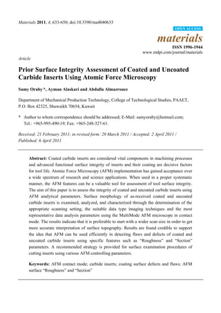
cutting edge. Edge deformation spreads over a relatively wide area and it is so severe that its depth is
extended through the three coating layers reaching the insert substrate. Data about this specimen will
be used later in the current study as AFM has been used to scan the deformed area at four different
locations as marked on the figure. In such situations, AFM techniques have a high potential for
integrity assessment at the micro and nano-scale of the surface. The atomic force microscope (AFM),
which was invented in 1986 by Binnig, Quate, and Gerber [12], has become an indispensable tool for
investigators in many fields applications; physical, chemical, tribologyical and mechanical materials
properties, biological sciences and, biomechanical and electromechanical. AFM uses a mechanical
probe with an ultra small tip to scan a surface sample in both X and Y directions and to sense the
corresponding vertical height Z, thereby generating a magnified, or three-dimensional images of
surfaces down to nanometer resolution, Figure 2. A feedback control system responds to those changes
by adjusting the tip-sample distance in order to maintain a constant deflection/ distance to the sample
surface [13]. It is essentially this vertical movement of the tip that translates into a topographical image
of the surface with accuracy of few µm or less. The main aim of this paper is to study and discuss the
integrity of coated and uncoated carbide inserts using AFM analytical parameters. This is to determine
the feasibility of using AFM features to establish an efficient firm and time saving testing routine for
use by tool researchers, designers, developers and quality controllers to improve the characteristics of
the manufactured inserts or to develop new advanced types.
Figure 1. Scanning electron microscopy (SEM) micrograph of the notch wear of one of the
coated carbide inserts used in this study.](https://image.slidesharecdn.com/paper8oraby-140808142420-phpapp02/85/Prior-Surface-Integrity-Assessment-of-Coated-and-Uncoated-Carbide-Inserts-Using-Atomic-Force-Microscopy-3-320.jpg)
![Materials 2011, 4 636
Figure 2. Basic tip movements in atomic force microscopy (AFM) [14].
2. Experimental Setup and Hardware Setting
Five as received inserts types were tested throughout the different stages of this study; two uncoated
and three multi-layer coated with a cemented carbide substrate, Figure 3. Technical specification of the
five types of inserts used in this study is listed in detail in Table 1. Inserts are of SPUN 12 03 12
configuration (thickness = 3.18 mm, r = 1.2 mm and l = 12.7 mm, clearance angle = 5–7 rake
angle = 6). To avoid possible testing scratches from AFM probe, a new sample was employed for each
scan run.
Figure 3. Types of employed coated and uncoated carbide inserts (cm scale with
mm subunits).
The NanoScope IV MultiMode Atomic Force Microscope (AFM) Scanning Probe Microscope
(SPM) in contact mode was used in this study. The contact mode was selected to suit the tribological
nature and the object of the current study. The NanoScope™ software [14] was used as a digital
control of the AFM processes. Software features allowed for all operations including preparation and
manipulation of the microscope before, during and after scanning (offline analysis procedures). To](https://image.slidesharecdn.com/paper8oraby-140808142420-phpapp02/85/Prior-Surface-Integrity-Assessment-of-Coated-and-Uncoated-Carbide-Inserts-Using-Atomic-Force-Microscopy-4-320.jpg)

![Materials 2011, 4 638
groove was detected. This surface imperfection is basically due to some improper manufacturing or
preparation and finishing (grinding) procedures. The depth of the groove is detected by the analysis,
sample 2, Table 2, to be as deep as 810 nm. Such defects may degrade the insert surface finish and,
consequently affects its performance whether it is used as a plain (uncoated) insert or is prepared for
further coating process. Also, Figures 7–9 explain similar micrographs to explain the possible
existence of defects in the coating layers. Figure 10 shows the SEM micrographs of many forms of the
observed surface defects such as: droplet, spallation, delamination and macroparticles of the coating
layer. Figure 10c shows a SEM micrograph for GC415 coated inset, sample 2, Table 3, where frequent
droplets were observed on the surface of the insert. The droplet configuration is better visualized and
further analyzed using the appropriate combination of data type and scan size.
The images indicate the existence of mutual interaction between Deflection and corresponding
Friction images as tip of the probe usually exhibits tilting laterally when it moves along the scanning
direction. Generally, it can be concluded that the Height data type produces an absolute judgment of
the surface roughness over the entire area along the scanned direction while Friction data introduces an
attractive indication about the roughness pattern in the lateral direction. Practically, it can be stated that
the captured Height data is preferable for surfaces that exhibit regularly distributed fingerprint
topography with less waviness and disturbances. This is supported in what was recommended by [14],
that in most instances, Height data type usually ensures an accurate topographical view.
Figure 4. Three dimensional Height images for different scan sizes for K68 uncoated
carbide inserts of (a) 2 μm; (b) 6 μm and (c) 12 μm.
(a) (b)
(c)](https://image.slidesharecdn.com/paper8oraby-140808142420-phpapp02/85/Prior-Surface-Integrity-Assessment-of-Coated-and-Uncoated-Carbide-Inserts-Using-Atomic-Force-Microscopy-6-320.jpg)

![Materials 2011, 4 640
3.2. Determination of the Appropriate Scan Size
To determine the most informative captured data, each specimen was independently scanned using
three different scan sizes; 2, 6 and 12 μm (as a limiting AFM capacity), Figures 4–9. As shown in
Figure 4, the extent of the surface defect (recess, Figure 10a) was precisely described by the widest
scan size of 12 μm. Some features would be lost when smaller scan sizes, Figures 4a, and b, were
considered. The same conclusion was reached regarding the existence of the droplet defect on the
surface of sample 2, Table 3. A full configuration of the droplet flaw was clearly described using
12 μm scan size in comparison to what was obtained by smaller scan sizes or by SEM micrograph,
Figure 10a. Generally, the use of a wider scan size usually produces more common, integrated and
more informative view of the surface topography. This is usually accompanied with adequate details
permitting the proper examination and the detection of the relatively wide surface defects and its
complete waviness measure [15,16]. Therefore, as a general rule, it is better to start an investigation
with the widest scan size available. In situations, however, a smaller scan size can be useful to provide
some nanoscale characteristics of the intended surface.
Figure 7. Three dimensional Height images for different scan sizes for GC435 coated
carbide inserts of (a) 2 μm; (b) 6 μm and (c) 12 μm.
(a) (b)
(c)](https://image.slidesharecdn.com/paper8oraby-140808142420-phpapp02/85/Prior-Surface-Integrity-Assessment-of-Coated-and-Uncoated-Carbide-Inserts-Using-Atomic-Force-Microscopy-8-320.jpg)

![Materials 2011, 4 642
Figure 10. SEM surface micrograph showing defects of the uncoated and multilayers
coated carbide inserts. (a) surface groove (K68, sample 2); (b) high surface roughness
(K68, sample 4); (c) droplets of coating spallation and delamination (GC415, sample 2).
(a) (b)
(c)
3.3. Data Analysis Techniques
A wide variety of analysis functions are available from the ―Analyze‖ menu in the off-line mode of
Nanoscope software [14] and, in the current study, only parameters relevant to surface tribological
aspects are extracted and elaborated. Investigated parameters include the ―Roughness‖ command and
the informative ―Section‖ command.
3.3.1. ―Roughness‖ Analysis Parameter of Surface Topography
The ―Roughness‖ parameter generates a wide variety of statistics of the surface topographical
aspects including classical roughness values, peak and summit texture data and surface area
calculations for the entire image. Among the many parameters available in the ―Roughness‖ analysis,
four relevant measures are selected to analyze the captured data. The four measures are the ―Average
roughness‖ Ra, the ―Image RMS‖ (Rq), the ―Image area difference %‖ and the image ―Z-range‖.
Analysis and results considering the above mentioned four basic roughness parameters accompanied
by their associated qualitative three-dimensional thumbnails are listed in Tables 2 and 3. Table 2 lists
the values of the four measured roughness parameters for K68 and K21 uncoated inserts. Among the
four scanned samples of K68 uncoated carbides (Samples 1–4), all parameters values support the idea](https://image.slidesharecdn.com/paper8oraby-140808142420-phpapp02/85/Prior-Surface-Integrity-Assessment-of-Coated-and-Uncoated-Carbide-Inserts-Using-Atomic-Force-Microscopy-10-320.jpg)
![Materials 2011, 4 643
that sample 3 is a normal defect-free specimen and it can be considered as a reference for the rest of
the samples. A SEM micrograph of sample 4 is shown in Figure 10b where high rough disturbances
dominated the entire surface of the insert. In comparison to the counterpart values for the normal
sample 3, all parameters are of much greater levels reaching 350%, 2,300%, 157% and 146% increase
for Z-range, area difference %, Rq and Ra, respectively. For sample 2, Table 3, that is shown by the
SEM micrograph, Figure 10a, corresponding values were about 76%, 20%, 128% and 119%. These
values, in comparison to those for sample 4, indicate that, in some situations where localized defects
dominate, sample 2, relative assessment is not accurate enough and more analysis using the most
appropriate and specific parameter is required. This remark is supported by the wide variation in the
values of roughness measures of K21 uncoated carbides, samples 1–2, Table 2. Whereas, for sample 2,
a localized surface defect exists, the surface topography is better represented either by Ra or Rq.
Table 3 lists values of the roughness parameters for the coated GC415 inserts including four intact
samples (samples 1–4) in addition to one worn insert (sample 5). For the same worn specimen
sample 5, four scans were performed on some preselected locations defined by positions 1 to 4 as
shown in Figure 1. When the values of each of the four roughness parameters of such a sample were
compared to the corresponding reference values, as the average mean of the measures of samples 1–4,
the percent increases were found to be; 1,400%, 18.6%, 202% and 154% for Z-range, area diff.%, Rq
and Ra, respectively. As shown in Figure 1, wear mode was of rubbing nature giving a misleading
indication of surface roughness improvement. However, for positions 2 and 3 (sample 5, Table 3), the
wear mode is of an irregular nature that is interpreted as increasing the levels of all the roughness
measures considered. This limits the feasibility of using AFM analysis for the worn specimen and, the
use of a different examination technique such as SEM is preferred.
3.3.2. ―Section‖ Analysis of Surface Topography
The ―Section‖ feature in NanoScope software offers a useful tool to quantitatively investigate the
topography of the surface localized defects [14]. Figure 11 shows the use of the ―Section‖ command
for the K68 uncoated carbide samples 1–3, Table 2, using the ―Height‖ two-dimensional image with
12 μm scan size. Three horizontal reference lines were allocated to provide information about the
surface topography over different locations of the scanned area. More features than those provided by
―Roughness‖ parameters were obtained including the width and the frequency of the existing flaws.
For instance, in Figure 11b, the groove width was determined to be of 3 μm regular width.
As shown in Figure 11c, data for the defective sample 4 reveals a height range of 1.5 μm comparing
to 0.5 μm for the reference sample 3, Table 2.
In order to get more information about the configuration of the droplet defect on the surface of the
GC415 coated sample 2, Table 3, both horizontal and diagonal sectioning reference lines were
allocated, Figure 12. It is shown that the droplet is of approximate elliptical shape with about 3 and
6 μm diagonals. Also, graphs indicate that within the scanned area, there is only one droplet
occurrence on the scanned area (unity frequency).
As shown in Figures 11 and 12, the accompanied table at the bottom of each graph provides some
useful information about the marked surface area being examined.](https://image.slidesharecdn.com/paper8oraby-140808142420-phpapp02/85/Prior-Surface-Integrity-Assessment-of-Coated-and-Uncoated-Carbide-Inserts-Using-Atomic-Force-Microscopy-11-320.jpg)


![Materials 2011, 4 648
In the majority of situations many analysis features are concomitantly provided and the preference
among them usually requires user technical intervention. Independent technical opinions should be
based on the functional objectives set by designer and the decision makers. However, many technical
and practical relevant issues were raised throughout the experimental and analysis stages and these are
discussed in the following paragraphs.
As a general practical rule, the Z-range and Area Diff. % measures in ―Roughness‖ parameter
usually should be started in the first examination instant. These offer a good prior general indication
about surface topography and its quality. Whenever a regular roughness pattern is observed, with a
―spread out‖ nature all over the entire surface, many ―roughness‖ measures can be beneficial to
determine the general characteristics of the topography. When manufacturing imperfections are
observed, the height range in the ―Section‖ should be of choice.
However, when worn surfaces are examined using AFM/SPM, the surfaces are always deformed in
various rubbing, hardening and chipping modes [17-19]. In such situations, surface topography tends
to have longer wavelength with small random asperities and, in general, roughness analysis may offer
little relevant information. Further examination procedures using SEM or even high sensitivity light
microscopy can be more feasible. Nevertheless, it is found that the ―Height‖ range in ―Section‖ can
provide some useful information regarding the severity and the nature of the developed wear mode.
Although, in the current study, several types of surface defects and flaw of coated and uncoated
carbide inserts were detectable, the criticality of these defects and flaws are not apparent and cannot be
claimed. Therefore, it is beneficial especially with the development of the AFM to assess the integrity
of coatings by finding out the failure initiation factors for the coating layers and the role of these
surface defects. Such studies can provide benchmarks for the different types of failure mechanisms and
provide an important insight for quality assurance of coating.
Table 4. The specification of the five coated and uncoated inserts used in this study.
Seq.
Type of surface
Imperfections
Roughness data Section Data
Hardware and
Software Setting
Zrange
(nm)
Area
Diff. %
Rq
(nm)
Ra
(nm)
Sp.
RMS
(nm)
Height
Range
(nm)
1
Preliminary surface
examination
• • •
a) Use at least three
different samples.
b) Use maximum
available scan size.
c) Use ―Height‖ image.
2
Normal defects free
surface
• • • •
3
Regular widespread
roughness pattern
• • • •
4
Tiny localized
surface defects
• • •
a) Compare with
normal reference
topography (Proced. 2).
5
Manufacturing
coating
imperfections
• •
6 Worn edge • •
a) Further SEM or/and
OM is preffered.](https://image.slidesharecdn.com/paper8oraby-140808142420-phpapp02/85/Prior-Surface-Integrity-Assessment-of-Coated-and-Uncoated-Carbide-Inserts-Using-Atomic-Force-Microscopy-16-320.jpg)


This study evaluates the surface integrity of coated and uncoated carbide inserts using Atomic Force Microscopy (AFM) to assess their morphology and detect defects. Results indicate that AFM is effective in identifying flaws, providing insights through data types such as height and friction, while emphasizing the importance of scan size for accurate surface characterization. A systematic approach is proposed for utilizing AFM parameters to enhance the quality control of cutting inserts in machining applications.


![Ceramic coating [tio2 zro2] on aluminium 6061 t6 for anti](https://cdn.slidesharecdn.com/ss_thumbnails/ceramiccoatingtio2-zro2onaluminium6061t6foranti-140821045215-phpapp01-thumbnail.jpg?width=640&height=640&fit=bounds)


![Attack surfaces and attack tress[inform]](https://cdn.slidesharecdn.com/ss_thumbnails/lecture03-260108015941-a4dee53b-thumbnail.jpg?width=640&height=640&fit=bounds)


