Download to read offline


![IJRET: International Journal of Research in Engineering and Technology eISSN: 2319-1163 | pISSN: 2321-7308
_______________________________________________________________________________________
Volume: 04 Issue: 03 | Mar-2015, Available @ http://www.ijret.org 88
5. CONCLUSION
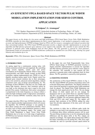
FPGA based Space vector PWM implemented, which
involves digital controller implementation. The digital
controller executed the algorithm for reference vector signal
to the controller. The PLL generator generated pulse width
modulation clock for three phases. The SVPWM based
method achieves a resolution of 1ns in the low-cost FPGA It
is concluded that solution have good linearity and
monotonicity properties.
REFERENCES
[1] Prodic, D. Maksimovic, and R. W. Erickson, “Design
and Implementation of a DigitalPWM Controller for
a High-Frequency Switching DC-DC Power
Converter,” The 27th
Annual Conference of the IEEE
Industrial Electronics Society, IECON 2001, Vol.
[2] R.F. Foley, R.C. Kavanagh, W.P. Marnane and M.G.
Egan, "A versatile digital pulsewidth modulation
architecture with area-efficient FPGA
implementation." Power Electronics Specialists
Conference, PESC 2005.
[3] V. Yousefzadeh, T. Takayama, D. Maksimovic.
"Hybrid DPWM with digital delay-locked loop."
IEEE Computer in Power Electronics Workshop,
COMPEL 2006.
[4] S.C. Huerta, A. de Castro, O. García, J.A. Cobos.
“FPGA based digital pulse width modulator with time
resolution under 2 ns.” IEEE Tran. on Power
Electronics, Vol. 23, No. 6, November 2008.
[5] Óscar López, Jacobo Álvarez, Jesús Doval-Gandoy,
and Francisco D. Freijedo, “Multilevel Multiphase
Space Vector PWM Algorithm”, IEEE
TRANSACTIONS ON INDUSTRIAL
ELECTRONICS, VOL. 55, NO. 5, pp. 1933-1942,
MAY 2008.](https://image.slidesharecdn.com/anefficientfpgabasedspacevectorpulsewidthmodulationimplementationforservocontrolapplication-160830114730/85/An-efficient-fpga-based-space-vector-pulse-width-modulation-implementation-for-servo-control-application-5-320.jpg)

The document presents the design of a low power and high performance FPGA-based Space Vector Pulse Width Modulation (SVPWM) controller for servo control applications. It details the implementation of a digital controller and a PLL generator to achieve accurate pulse width modulation for three-phase systems, emphasizing its advantages such as high precision control, low harmonic distortion, and reduced hardware requirements. Experimental results demonstrate effective performance with a resolution of 1ns, indicating good linearity and efficiency in FPGA utilization.