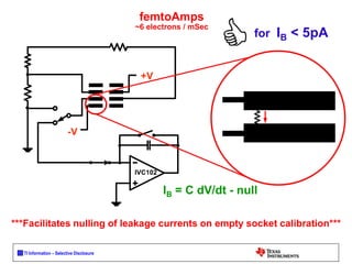
TI Information – Selective Disclosure
Testing
Op Amps and Comparators
Daryl Hiser
PA Op Amp -Test
TI Information – Selective Disclosure
Op Amps, Comparators, and
Pattern Based Testing……oh my!
TI Information – Selective Disclosure
Outline
• Basics of testing Op Amps.
– The Loops
– The Tests
• Pattern Based Testing.
• Basics of testing comparators.
• Beware of flying monkeys!
(common errors, issues, things to watch for)
TI Information – Selective Disclosure
Op Amp Loops
• If you can measure Vos well, most of the Op amp test
battle is won! PSRR, CMRR, AOL, Drift… are just looking
for changes in Vos as some parameter is varied.
• We use “test loops” to facilitate measurement and control
of op amps during test. The loop gives local gain of the
offset measurement.
• This presentation will evaluate two useful loop methods:
- False Summing Junction
- Two Amp Loop
TI Information – Selective Disclosure
Eagle Op Amp HIB
TI Information – Selective Disclosure
Op Amp test loops
DUT
100K
1K
100K
100K
Vout
+
-
101(Vos)
Loop
Drive
Vos
i = Vos / 1K
100 Vos
(False Summing Junction)
+10V
~ -10V
Offset Correction Factor = ACL + AFS
Vo = -(Vi + Vos(O.C.F))
+ -
+ -
TI Information – Selective Disclosure
Op Amp test loops
DUT
100K
1K
100K
100K
Vout
+
-
Loop
Drive
(False Summing Junction)
+10V
-9.698V
Offset Correction Factor = ACL + ASJ
Vo = -(Vi + Vos(O.C.F))
+ -
+ -
1mV
101mV
+
-
i2 = 98.99µA
i1= 1µA
i3 = 97.99µA
ACL = 200K/1K + 1 = 201
ASJ = 100K/1K + 1 = 101
OCF = 302
+10.302V
102.01µA 101.01µA
-10.0V
TI Information – Selective Disclosure
Op Amp test loops
DUT
100K
1K
100K
100K
Vout
+
-
101(Vos)
Loop
Drive
(False Summing Junction)
Pro’s
• Simple
• Stable
• Small (4 tiny surface
mount resistors
and you can test
everything but IB
Con’s
• Feedback R is a Load
• Loop drive a function of
DUT Vos.
The worse the DUT’s DC precision the more significant loop errors become.
TI Information – Selective Disclosure
Null
Amp
DUT
Loop
Drive
10K
1nF
10K
100Ω
25pF
Vout
Op Amp test loops
(2 Amp Loop)
Vos
i = Vos / 100
100 Vos
+10V
+10V
Pro’s
• No Load Current
• Loop drive is
independent
from DUT Vos
Con’s
• More complex
• Requires
Compensation!!
Type 1
Type 2
101 Vos
TI Information – Selective Disclosure
Bode plot for 2 Amp Loop
(uncompensated)
20
40
60
80
100
120
140
160
180
200
220
240
10M
1M
100K
10K
1K
100
10
1
0.1
0.01
Frequency Hz
Gain
dB
Closed loop Gain
ACL
(100K/100) +1 = 1001
or ~ 60dB
ACL
40db/decade
closure!
Null
Amp
DUT
Loop
Drive
2K
100K
100Ω
Vout
Combined response
Both Amps
Null Amp
DUT
TI Information – Selective Disclosure
Type 2 compensation
20
40
60
80
100
120
140
160
180
200
220
240
10M
1M
100K
10K
1K
100
10
1
0.1
0.01
Combined response
Both amps
40db / decade
Frequency Hz
Gain
dB
ACL
20db/decade
closure!
Null
Amp
DUT
Loop
Drive
2K
100K
100Ω
Vout
CF = 1 / (20KHz x 100KΩ x 2π) = 80pF
80pF
TI Information – Selective Disclosure
Type 2 compensation range
20
40
60
80
100
120
140
160
180
200
220
240
10M
1M
100K
10K
1K
100
10
1
0.1
0.01
Frequency Hz
Gain
dB
ACL
Optimum compensation
Lowest pole frequency
Highest pole frequency
TI Information – Selective Disclosure
Bode plot for Type 1 comp.
20
40
60
80
100
120
140
160
180
200
220
240
10M
1M
100K
10K
1K
100
10
1
0.1
0.01
Frequency Hz
Gain
dB
Closed loop Gain
ACL
(100K/100) +1 = 1001
or ~ 60dB
20db/decade
closure!
Null
Amp
DUT
Loop
Drive
2K
100K
100Ω
Vout
100pF
TI Information – Selective Disclosure
Type 1 Compensation Range
20
40
60
80
100
120
140
160
180
200
220
240
10M
1M
100K
10K
1K
100
10
1
0.1
0.01
Frequency Hz
Gain
dB
ACL
TI Information – Selective Disclosure
Null
Amp
DUT
Loop
Drive
10K
1nF
10K
100Ω
25pF
Vout
TI Information – Selective Disclosure
Type 1 compensation
Given Rf, Rin, Rc, BW1
Type II compensation
Given Rf, Rin, BW1, BW2:
Amp2
Amp1
Loop
Drive
Rc
Type I
Rf
Rin
Type II
TI Information – Selective Disclosure
Op Amp testing basics
Key Parameters Abbr.
Continuity / Contact resistance Cres
Quiescent Current IQ
Input offset voltage VOS
Power Supply Rejection PSRR
Common Mode Rejection CMRR
Open Loop Gain AOL
Short circuit current ISC
Slew Rate SR
Gain Bandwidth GBW
Input Bias current IB
Noise
Total Harmonic Distortion THD
TI Information – Selective Disclosure
18
Continuity ***1 current ***
Continuity is measured by sourcing a small current (100uA typ.) through
each IO pin through the ESD diodes to the positive supply, and then
sinking current through the diodes connected between the IO pins and
the negative supply. This verifies all ESD diodes are connected as well
as all wire bonds intact and some contact to each pin.
DUT
Vcc
Vee
Vout
APU
APU
APU
APU
APU
DUT
Vcc
Vee
Vout
APU
APU
APU
APU
APU
i1 = 100µA
i1 = 100µA
TI Information – Selective Disclosure
19
Contact Resistance ***2 currents***
CRES is measured between each supply and the output using 10mA and
15mA currents to get past the diode I/V knee. It is a bulk resistance
includes 2 contact resistances and the internal diode resistance.
Cres1 = (Rp1 + Rp2) = [(V1 – V2)/ (I1 – I2) ] – Rd1
Cres2 = (Rp2 + Rp3) = [(V1 – V2)/ (I1 – I2) ] – Rd2
Contact resistance > ~1Ω can be accounted for using this method.
If 1Ω or less is a problem for measurements, Kelvin contacts should be used.
DUT
APU
Rp1
Rp2
Rp3
Rd2
Rd1
Cres3 = (Rp1 + Rp3) = [(V1 – V2)/ (I1 – I2) ] – Rd3
i1 = 10mA
i2 = 15mA
0
10
20
30
40
50
0.0 0.2 0.4 0.6 0.8 1.0
Current
(mA)
Junction Voltage (V)
Diode I-V Curve
TI Information – Selective Disclosure
Complete Diode Equations
   
   
 
 
   
 
 
15
.
273
ln
ln
ln
ln
ln
ln
5
5
35
35
35
35
85
85
35
85
5
35
5
35
35
85
35
85
5
35
5
35
35
85
35
35
85
85
5
5
35
35
5
35
35
85
35
35
85
85
5
5
35
35























































































B
E
B
E
B
E
B
E
E
E
E
E
BE
BE
BE
BE
E
E
E
E
E
E
E
E
B
E
B
E
B
E
B
E
BE
BE
BE
BE
B
E
B
E
B
E
B
E
S
I
I
I
I
I
I
I
I
I
I
I
I
V
V
V
V
I
I
I
I
nk
q
e
Temperatur
I
I
I
I
I
I
I
I
I
I
I
I
V
V
V
V
I
I
I
I
I
I
I
I
R
CRES and temperature ***3 currents***
i1 = 5µA
i2 = 35µA
i3 = 85µA
Temperature accuracy ~ ± 5°C with ESD diode
CRES
and
Temperature
DUT
APU
Rp1
Rp2
Rp3
Rd2
Rd1
TI Information – Selective Disclosure
21
Quiescent current / Integrity / ISC
Null
Amp
DUT
Loop
Drive
Vcc
Vee
Rf
Rg Vos(Rf/Rg)+1
Iq = Iq(meas) – empty socket null
One note of caution…beware of measuring load current
by looking at the change from Quiescent current on the DUT
supplies.
ibias
iOUT = 1mA
1mA
1mA
1.5mA
0.5mA
Output stage
TI Information – Selective Disclosure
22
Vos / PSRR / CMRR
PSRR = ΔVos / ΔVcc (μV/V) CMRR = ΔVos/ ΔVcm (μV/V)
Null
Amp
DUT
Loop
Drive
2K
1nF
10K
100Ω
25pF
CMV
Drive
Vos(Rf/Rg)+1
(101)
If (Ib x RF)/100 is significant to Vos it must be considered!
Beware of oscillations… Op Amps “may” rectify low level oscillations
because of input clamping diodes and this can appear as an erroneous
offset voltage.
± CMV
ΔVcc
ΔVee
TI Information – Selective Disclosure
Example of big IB error on Vos measurement
DUT
100K
1K
100K
100K
Vout
+
-
Loop
Drive
1mV
500nA
1µA
= 150mV /loop gain = 1.5mV
50% error!!!
Smaller resistors reduce error.
ie 10K and 100Ω would be 50uV error…
or Measure IB first and use it in
Vos calculation.
In this configuration there is a 1µV / nA error on Vos.
The 2 Amp loop with same R values would have the same
error!
1.5µA
101(Vos) + ib x 100KΩ
TI Information – Selective Disclosure
24
CMRR considerations
1V
5V
5V
-5V
-5V -9V
9V
-1V
4V
-4V
=
=
-4V
0V
4V
0V
•Moving supplies and
output is equivalent to
moving common mode
voltage !
• Remember that you
can not short the inputs
of an Op Amp together.
Doing so will put it in
the rail !!!
TI Information – Selective Disclosure
Vos
2.75
-2.75 Vcc-1.4V
Transition
region
pMos active nMos active
VCM
25
PSRR consideration for rail to rail amps
-0.6V -0.6V
CMV1 CMV2
CMV2
CMV1
0.9V
-0.9V
2.75 V
-2.75 V
0.9 V
-0.9 V
pMos to nMos
transition
TI Information – Selective Disclosure
26
AOL / Swing / Slam
Aol = ΔVos / ΔVout (μV/V)
Null
Amp
DUT
Loop
Drive
Vcc
Vee
Rf
Rg
RL Vos(Rf/Rg)+1
Vout
TI Information – Selective Disclosure
Swing Aol / Slam considerations
Vout
Vos
Vcc
Vee
+Swing +Slam
-Swing
-Slam
- Precision in drive for swing….”just enough”
- Compare Vout to supplies…not ground
- Remember RF in || with RL in FSJ
AOL Curve
Swing limit Slam limit Vcc
Vout
Vos
TI Information – Selective Disclosure
Slew Rate
DUT
100K
1K
100K
100K
Vout
+
-
101(Vos)
Loop
Drive
Fast Digitizer
Or
Window
Comparator
2K
Fast Source
Or
Fast Switch
• Slew of source must be faster than DUT
• DUT slew should not be limited by parasitic RC’s
• Some Op Amps are specified in unity gain…
TI Information – Selective Disclosure
Gain Bandwidth Product
GBP = test frequency * [Vout(rms) / Vos(rms)]
DUT
100K
1K
100K
100K
Vout
+
-
101(Vos)
Peak to Peak
or
RMS Meter/
Digitizer
AWG
The test frequency should be 2x Unity Gain BW / loop gain
TI Information – Selective Disclosure
Bode plot of gain vs frequency
20
40
60
80
100
120
10M
1M
100K
10K
1K
100
10
1
Frequency
Gain (db)
• As frequency increases,
parasitics may begin to
dominate!
The higher bandwidth the greater the challenge!
LG = 100
LG = 1000
Test frequency
Open Loop
Loop 1K
Loop 100
TI Information – Selective Disclosure
The dreaded iB test…
IB hurts even
my head
“It’s like trying to poke a cat out from under the porch with a rope”
-Unknown-
TI Information – Selective Disclosure
Some IB issues and challenges
µA down to fA
Stability
(Thermal EMFs)
Leakages
Humidity
Environmental noise
…
TI Information – Selective Disclosure
nanoAmps
IB = ΔV / Loopgain / Rib
for IB greater than ~200pA
DUT
100K
IB
RIB
VM
• Ios = Ib+ - Ib- (math not measure)
• Current into the input is “positive”
by convention.
• identical currents will produce
opposite changes in “vos”
measurement… Ib+ gets multiplied
by -1.
TI Information – Selective Disclosure
picoAmps
IB = C dV/dt / Loopgain
for IB 5pA to ~200pA
DUT
100K
1K
100K
IB
Cint
TI Information – Selective Disclosure
femtoAmps
~6 electrons / mSec
IVC102
-V
+V
for IB < 5pA
***Facilitates nulling of leakage currents on empty socket calibration***
IB = C dV/dt - null
TI Information – Selective Disclosure
I = C(dV/dt)
∆V
∆T
Step 1:
Run an open socket leakage test for
each amplifier input and store values
Step 2:
Measure bias current of each input
Step 3:
Bias Current = IMEASURED – ILEAKAGE
Leakage
Leakage + IB
TI Information – Selective Disclosure
Important considerations for low IB measurements
• Low leakage Capacitor
( Teflon, glass,
polypropylene
polystyrene).
• Low thermal EMF
cancelled, mechanical
latching relays w/ active
high drivers.
DUT
Ib
Cint
VEMF
R
KIDEAL VEMF
R
KIDEAL
TI Information – Selective Disclosure
DUT
100K
1K
100K
100K
Vout
+
-
101(Vos)
Loop
Drive
-
+
Thermal emfs are indistinguishable from Vos
Thermal emf
Vos
Vos + emf
i = (Vos +emf)1K
TI Information – Selective Disclosure
Thermal emfs
DUT
100K
1K
100K
100K
Vout
+
-
101(Vos)
Loop
Drive
Thermal emfs inside
this ring cause 1:1 errors
Thermal emfs outside
this ring are divided by
the loop gain!!!
TI Information – Selective Disclosure
Back to Low IB
Active High vs Active Low drivers
VRelay
Control
Relay
Coil
VRelay
Control
Relay
Coil
Active High Driver Active Low Driver
Low thermal EMF cancelled, mechanical latching relays w/ active high drivers.
TI Information – Selective Disclosure
COIL
12 V
C int
Active High Drive
COIL
12 V
C int
Open Collector
RELAY RELAY
Ib
Ib
Relay Drivers
DUT
Ib
Cint
TI Information – Selective Disclosure
COIL
12 V
C int
Active High Drive
COIL
12 V
C int
Open Collector
RELAY RELAY
Ib
Ib
Relay Drivers
DUT
Ib
Cint
TI Information – Selective Disclosure
COIL
Relay Drivers
12 V
C int
Active High Drive
COIL
12 V
C int
Open Collector
RELAY RELAY
Ib
Ib
DUT
Ib
Cint
TI Information – Selective Disclosure
• Actively High driven Latching relays reduce:
– Leakage (Coil Voltage) during test. (Good for Low IB)
– Heating (Coil current) during test (Good for Low Vos)
– EMI (Coil B field) during test (Good for both)
DUT
• Exposed guard traces reduce surface leakage!
Relay Drivers
Guard traces / Shielding
DUT
Buf
Active guarding can further reduce
leakage but adds complexity
TI Information – Selective Disclosure
Guard traces / Shielding
Exposed
Guard traces
High Z trace
TI Information – Selective Disclosure
Guard traces / Shielding
• Internal Guarding and Shielding (cross section )
grounded guard traces
FR4 material
Ground planes
Protected trace
TI Information – Selective Disclosure
“Two for one”
~One integration time -> 2 ib measurements Ibn = C [(M4 – M1) / T1]
Ibp = C [(M3 – M2) / T2]
TI Information – Selective Disclosure
Current Ib Test Investigation
• We are designing an octal site board with a different
Ib measurement experiment on each site for the purpose
of improving our understanding and techniques.
• We plan to contact our National counterparts to see if
they have any helpful practices or techniques that we
could leverage or adopt.
• If you have any suggestions or ideas, I would love to
hear them!!
TI Information – Selective Disclosure
Getting close…
TI Information – Selective Disclosure
 What is pattern based testing?
 Why bother?
 How can you implement it?
TI Information – Selective Disclosure
PBT: Overview
Post-process data in DSP memories! Avoid *slow* data transfer!
TI Information – Selective Disclosure
Digging a bit deeper for Op Amp Testing
• Predefined
waveforms are
generated.
• One circuit
configuration is
selected that is
most suitable for
all tests
• The output is
digitized and
stored
• Digitized data is
analyzed
TI Information – Selective Disclosure
Pattern Based Testing: Analysis
Typical Segment • Each test segment is
composed of 2
elements:
– Settling time
– Measuring time
• Analysis of the raw
data will allow for
correct time selection
• This alone can
reduce test times!
10/9/2022 “TI Proprietary Information - Strictly Private” or similar placed here if applicable
Settle Measure
TI Information – Selective Disclosure
Raw data Analysis
• Raw data analysis provides many of benefits
• The current testing methodology would not show all of the raw data.
Only 1 averaged point would be returned.
• Debugging and verification can be improved by viewing the raw data!
10/9/2022 54
Slight oscillation on some units. Adjust
compensation. Perfect!
TI Information – Selective Disclosure
PBT Benefits
• Reduced test time 1.5 seconds to 0.3 seconds
• Reduced Test % of COB
• More thorough coverage at probe and FT
Where do the time savings come from?
TI Information – Selective Disclosure
Quiz
On the Eagle tester, how long does it take 8 QMS’s grouped together
to make a measurement if the number of samples is 100 and the
sample time is 10uS?
qmsmv( QMS_GP, QMS_PREC, 100, 10 );
Answer: ~ 9mS
TI Information – Selective Disclosure
A comparison: Discrete vs PBT on ETS364’s
Action Group time cost
Control APU Group (Vcc) 8mS
Control APU Group (Vee) 8mS
Control APU Group (Vcm) 16mS
Control APU Group (Vout) 16mS
Control Dpins ?
Control Cbits ?
Settling time ?
Control QMS Group 8mS
~60mS
x discrete setups ( 11 )
Total “Setup” Time 660mS
Action Group time cost
Control APU Group (Vcc) 8mS
Control APU Group (Vee) 8mS
Control APU Group (Vcm) 16mS
Control SPU Group (Vout) 16mS
Control Dpins ?
Control Cbits ?
Settling time ?
Control QMS Group 8mS
~60mS
x patterns (1-4)
Total “Setup” Time 60 - 240mS
TI Information – Selective Disclosure
Future Work
• Continue to refine the SW and analysis tools
• Final Test implementation
• Hardware improvements to support method
• Expanding test coverage … Noise, Settling time, Drift?
TI Information – Selective Disclosure
Whaddaya mean
you can’t test
prop delay?
I want it out this week!
Comparators
TI Information – Selective Disclosure
Comparator Test
 Similar to Op amps, if you can measure Vos, you are most of the way
there on comparators… and there are many ways to do this.
• Continuity
• Quiescent Current
• Vos
• Psrr
• Cmrr
• Output Swing
• Output current
• Bias Current
• Slew Rate aka
rise time/ fall time
• Propagation delay
• Hysteresis
 Most Comparators are not “stable” in a loop like an op amp.
 No loop gain means precision Vos measurements need a different
strategy.
TI Information – Selective Disclosure
Vos / PSRR / CMRR
10KΩ
1KΩ
AWG
Digitizer
Vcc
Vee
Synchronous
*May need to buffer
and or filter.
Attenuator reduces AWG error
(drift, offset, lsb)
and potentially noise.
TI Information – Selective Disclosure
Vos / PSRR / CMRR
10KΩ
1KΩ
AWG
Timer
Vcc
Vee
Asynchronous
Just arm timer and
run AWG
TI Information – Selective Disclosure
Vout
Time
V1
V2
Vin
Vos = (V1 + V2 ) /2 Vos = Vin(max) - (t2 – t1) /2 * dv/dt
t1 t2
or
Consider ramp speed and propagation delay vs test time!
ΔV = 2 x propagation
delay*
Vos
ΔV
*Propagation delay of “system”
TI Information – Selective Disclosure
Hysteresis
Vout
Time
V1
V2
Hysteresis
Vin
A Vos measurement on a comparator with hysteresis requires
a synchronous method or a one shot that is coupled to a
sample and hold or triggers a measurement.
TI Information – Selective Disclosure
Propagation delay
DUT
Pedestal
DAC
Fast
Edge
Timer
Counter
(TMU)
•Limited by accuracy and or resolution of the timer / counter.
ie QTMU accuracy is ~100pS with ~10pS resolution.
• Trace lengths, attention to parasitics in layout become a big
factor for fast prop times. Speed of the “fast edge” is also a
factor. Many comparators have asymetric prop. delays
Compare to shunt to make
measurement “delta”
TI Information – Selective Disclosure
Propagation delay timing
time
volts
input
output
PDH PDL
TI Information – Selective Disclosure
Propagation delay
A cool circuit that might work… a ring oscillator
DUT
Timer
Counter
(TMU)
Monostable
multivibrator
-
Pedestal
•RC determines the oscillation frequency.
tPD = (time)/ Δcounts/2
shunt
tPD = Δtime/counts/2
or the time for fixed number of counts.
•Can measure the number of counts for fixed time period
TI Information – Selective Disclosure
TINA says “looks good”
• Without Comparator in the loop:
• Number of count (Nc): 2 ^ 8 (8-bit binary count)
• Total Time (Tc): 40.99us
• T1 (=Nc/Tc) 160.1ns (Calculated) 160.4ns (Measured)
• With Comparator in the loop:
• Number of count (Nc): 2 ^ 8 (8-bit binary count)
• Total Time (Tc): 42.88us
• T2 (=Nc/Tc) 167.5ns (Calculated) 170.8ns (Measured)
• Prop Delay (T2 – T1)/2 = 3.7ns
Might be handy multisite testing where timing measurements need to be done serially!
TI Information – Selective Disclosure
hiser_daryl@ti.com
Special Thanks:
Matt Picket and
Yazdi Contractor
For their work on PBT
TI Information – Selective Disclosure
Needs
• Our implementation of Pattern Based testing utilizes added functionality
available only in the new ETS364 APU-12 resource. More AWGS and more
DSP’s and digitizers.
• Fortunately, APU-12’s are the roadmap for all new ETS systems purchased by
TI.
• Unfortunately, there are only two APU-12 systems available in TLAB for
development. *
* 5 more systems have been approved but are in
negotiation
as to the final configurations. (sans MPU’s possibly)
TI Information – Selective Disclosure
Vos
2.75
-2.75 Vcc-1.4V
Transition
region
pMos active nMos active
VCM
72
PSRR consideration for rail to rail amps
1.5V
-0.3V
3.35V
-2.15V
0.6V 0.6V
-0.6V -0.6V
CMV1 CMV2
CMV2
CMV1
0V
0V
TI Information – Selective Disclosure

Testing Op Amps and Comparators.pptx

  • 1.
    TI Information –Selective Disclosure Testing Op Amps and Comparators Daryl Hiser PA Op Amp -Test
  • 2.
    TI Information –Selective Disclosure Op Amps, Comparators, and Pattern Based Testing……oh my!
  • 3.
    TI Information –Selective Disclosure Outline • Basics of testing Op Amps. – The Loops – The Tests • Pattern Based Testing. • Basics of testing comparators. • Beware of flying monkeys! (common errors, issues, things to watch for)
  • 4.
    TI Information –Selective Disclosure Op Amp Loops • If you can measure Vos well, most of the Op amp test battle is won! PSRR, CMRR, AOL, Drift… are just looking for changes in Vos as some parameter is varied. • We use “test loops” to facilitate measurement and control of op amps during test. The loop gives local gain of the offset measurement. • This presentation will evaluate two useful loop methods: - False Summing Junction - Two Amp Loop
  • 5.
    TI Information –Selective Disclosure Eagle Op Amp HIB
  • 6.
    TI Information –Selective Disclosure Op Amp test loops DUT 100K 1K 100K 100K Vout + - 101(Vos) Loop Drive Vos i = Vos / 1K 100 Vos (False Summing Junction) +10V ~ -10V Offset Correction Factor = ACL + AFS Vo = -(Vi + Vos(O.C.F)) + - + -
  • 7.
    TI Information –Selective Disclosure Op Amp test loops DUT 100K 1K 100K 100K Vout + - Loop Drive (False Summing Junction) +10V -9.698V Offset Correction Factor = ACL + ASJ Vo = -(Vi + Vos(O.C.F)) + - + - 1mV 101mV + - i2 = 98.99µA i1= 1µA i3 = 97.99µA ACL = 200K/1K + 1 = 201 ASJ = 100K/1K + 1 = 101 OCF = 302 +10.302V 102.01µA 101.01µA -10.0V
  • 8.
    TI Information –Selective Disclosure Op Amp test loops DUT 100K 1K 100K 100K Vout + - 101(Vos) Loop Drive (False Summing Junction) Pro’s • Simple • Stable • Small (4 tiny surface mount resistors and you can test everything but IB Con’s • Feedback R is a Load • Loop drive a function of DUT Vos. The worse the DUT’s DC precision the more significant loop errors become.
  • 9.
    TI Information –Selective Disclosure Null Amp DUT Loop Drive 10K 1nF 10K 100Ω 25pF Vout Op Amp test loops (2 Amp Loop) Vos i = Vos / 100 100 Vos +10V +10V Pro’s • No Load Current • Loop drive is independent from DUT Vos Con’s • More complex • Requires Compensation!! Type 1 Type 2 101 Vos
  • 10.
    TI Information –Selective Disclosure Bode plot for 2 Amp Loop (uncompensated) 20 40 60 80 100 120 140 160 180 200 220 240 10M 1M 100K 10K 1K 100 10 1 0.1 0.01 Frequency Hz Gain dB Closed loop Gain ACL (100K/100) +1 = 1001 or ~ 60dB ACL 40db/decade closure! Null Amp DUT Loop Drive 2K 100K 100Ω Vout Combined response Both Amps Null Amp DUT
  • 11.
    TI Information –Selective Disclosure Type 2 compensation 20 40 60 80 100 120 140 160 180 200 220 240 10M 1M 100K 10K 1K 100 10 1 0.1 0.01 Combined response Both amps 40db / decade Frequency Hz Gain dB ACL 20db/decade closure! Null Amp DUT Loop Drive 2K 100K 100Ω Vout CF = 1 / (20KHz x 100KΩ x 2π) = 80pF 80pF
  • 12.
    TI Information –Selective Disclosure Type 2 compensation range 20 40 60 80 100 120 140 160 180 200 220 240 10M 1M 100K 10K 1K 100 10 1 0.1 0.01 Frequency Hz Gain dB ACL Optimum compensation Lowest pole frequency Highest pole frequency
  • 13.
    TI Information –Selective Disclosure Bode plot for Type 1 comp. 20 40 60 80 100 120 140 160 180 200 220 240 10M 1M 100K 10K 1K 100 10 1 0.1 0.01 Frequency Hz Gain dB Closed loop Gain ACL (100K/100) +1 = 1001 or ~ 60dB 20db/decade closure! Null Amp DUT Loop Drive 2K 100K 100Ω Vout 100pF
  • 14.
    TI Information –Selective Disclosure Type 1 Compensation Range 20 40 60 80 100 120 140 160 180 200 220 240 10M 1M 100K 10K 1K 100 10 1 0.1 0.01 Frequency Hz Gain dB ACL
  • 15.
    TI Information –Selective Disclosure Null Amp DUT Loop Drive 10K 1nF 10K 100Ω 25pF Vout
  • 16.
    TI Information –Selective Disclosure Type 1 compensation Given Rf, Rin, Rc, BW1 Type II compensation Given Rf, Rin, BW1, BW2: Amp2 Amp1 Loop Drive Rc Type I Rf Rin Type II
  • 17.
    TI Information –Selective Disclosure Op Amp testing basics Key Parameters Abbr. Continuity / Contact resistance Cres Quiescent Current IQ Input offset voltage VOS Power Supply Rejection PSRR Common Mode Rejection CMRR Open Loop Gain AOL Short circuit current ISC Slew Rate SR Gain Bandwidth GBW Input Bias current IB Noise Total Harmonic Distortion THD
  • 18.
    TI Information –Selective Disclosure 18 Continuity ***1 current *** Continuity is measured by sourcing a small current (100uA typ.) through each IO pin through the ESD diodes to the positive supply, and then sinking current through the diodes connected between the IO pins and the negative supply. This verifies all ESD diodes are connected as well as all wire bonds intact and some contact to each pin. DUT Vcc Vee Vout APU APU APU APU APU DUT Vcc Vee Vout APU APU APU APU APU i1 = 100µA i1 = 100µA
  • 19.
    TI Information –Selective Disclosure 19 Contact Resistance ***2 currents*** CRES is measured between each supply and the output using 10mA and 15mA currents to get past the diode I/V knee. It is a bulk resistance includes 2 contact resistances and the internal diode resistance. Cres1 = (Rp1 + Rp2) = [(V1 – V2)/ (I1 – I2) ] – Rd1 Cres2 = (Rp2 + Rp3) = [(V1 – V2)/ (I1 – I2) ] – Rd2 Contact resistance > ~1Ω can be accounted for using this method. If 1Ω or less is a problem for measurements, Kelvin contacts should be used. DUT APU Rp1 Rp2 Rp3 Rd2 Rd1 Cres3 = (Rp1 + Rp3) = [(V1 – V2)/ (I1 – I2) ] – Rd3 i1 = 10mA i2 = 15mA 0 10 20 30 40 50 0.0 0.2 0.4 0.6 0.8 1.0 Current (mA) Junction Voltage (V) Diode I-V Curve
  • 20.
    TI Information –Selective Disclosure Complete Diode Equations                     15 . 273 ln ln ln ln ln ln 5 5 35 35 35 35 85 85 35 85 5 35 5 35 35 85 35 85 5 35 5 35 35 85 35 35 85 85 5 5 35 35 5 35 35 85 35 35 85 85 5 5 35 35                                                                                        B E B E B E B E E E E E BE BE BE BE E E E E E E E E B E B E B E B E BE BE BE BE B E B E B E B E S I I I I I I I I I I I I V V V V I I I I nk q e Temperatur I I I I I I I I I I I I V V V V I I I I I I I I R CRES and temperature ***3 currents*** i1 = 5µA i2 = 35µA i3 = 85µA Temperature accuracy ~ ± 5°C with ESD diode CRES and Temperature DUT APU Rp1 Rp2 Rp3 Rd2 Rd1
  • 21.
    TI Information –Selective Disclosure 21 Quiescent current / Integrity / ISC Null Amp DUT Loop Drive Vcc Vee Rf Rg Vos(Rf/Rg)+1 Iq = Iq(meas) – empty socket null One note of caution…beware of measuring load current by looking at the change from Quiescent current on the DUT supplies. ibias iOUT = 1mA 1mA 1mA 1.5mA 0.5mA Output stage
  • 22.
    TI Information –Selective Disclosure 22 Vos / PSRR / CMRR PSRR = ΔVos / ΔVcc (μV/V) CMRR = ΔVos/ ΔVcm (μV/V) Null Amp DUT Loop Drive 2K 1nF 10K 100Ω 25pF CMV Drive Vos(Rf/Rg)+1 (101) If (Ib x RF)/100 is significant to Vos it must be considered! Beware of oscillations… Op Amps “may” rectify low level oscillations because of input clamping diodes and this can appear as an erroneous offset voltage. ± CMV ΔVcc ΔVee
  • 23.
    TI Information –Selective Disclosure Example of big IB error on Vos measurement DUT 100K 1K 100K 100K Vout + - Loop Drive 1mV 500nA 1µA = 150mV /loop gain = 1.5mV 50% error!!! Smaller resistors reduce error. ie 10K and 100Ω would be 50uV error… or Measure IB first and use it in Vos calculation. In this configuration there is a 1µV / nA error on Vos. The 2 Amp loop with same R values would have the same error! 1.5µA 101(Vos) + ib x 100KΩ
  • 24.
    TI Information –Selective Disclosure 24 CMRR considerations 1V 5V 5V -5V -5V -9V 9V -1V 4V -4V = = -4V 0V 4V 0V •Moving supplies and output is equivalent to moving common mode voltage ! • Remember that you can not short the inputs of an Op Amp together. Doing so will put it in the rail !!!
  • 25.
    TI Information –Selective Disclosure Vos 2.75 -2.75 Vcc-1.4V Transition region pMos active nMos active VCM 25 PSRR consideration for rail to rail amps -0.6V -0.6V CMV1 CMV2 CMV2 CMV1 0.9V -0.9V 2.75 V -2.75 V 0.9 V -0.9 V pMos to nMos transition
  • 26.
    TI Information –Selective Disclosure 26 AOL / Swing / Slam Aol = ΔVos / ΔVout (μV/V) Null Amp DUT Loop Drive Vcc Vee Rf Rg RL Vos(Rf/Rg)+1 Vout
  • 27.
    TI Information –Selective Disclosure Swing Aol / Slam considerations Vout Vos Vcc Vee +Swing +Slam -Swing -Slam - Precision in drive for swing….”just enough” - Compare Vout to supplies…not ground - Remember RF in || with RL in FSJ AOL Curve Swing limit Slam limit Vcc Vout Vos
  • 28.
    TI Information –Selective Disclosure Slew Rate DUT 100K 1K 100K 100K Vout + - 101(Vos) Loop Drive Fast Digitizer Or Window Comparator 2K Fast Source Or Fast Switch • Slew of source must be faster than DUT • DUT slew should not be limited by parasitic RC’s • Some Op Amps are specified in unity gain…
  • 29.
    TI Information –Selective Disclosure Gain Bandwidth Product GBP = test frequency * [Vout(rms) / Vos(rms)] DUT 100K 1K 100K 100K Vout + - 101(Vos) Peak to Peak or RMS Meter/ Digitizer AWG The test frequency should be 2x Unity Gain BW / loop gain
  • 30.
    TI Information –Selective Disclosure Bode plot of gain vs frequency 20 40 60 80 100 120 10M 1M 100K 10K 1K 100 10 1 Frequency Gain (db) • As frequency increases, parasitics may begin to dominate! The higher bandwidth the greater the challenge! LG = 100 LG = 1000 Test frequency Open Loop Loop 1K Loop 100
  • 31.
    TI Information –Selective Disclosure The dreaded iB test… IB hurts even my head “It’s like trying to poke a cat out from under the porch with a rope” -Unknown-
  • 32.
    TI Information –Selective Disclosure Some IB issues and challenges µA down to fA Stability (Thermal EMFs) Leakages Humidity Environmental noise …
  • 33.
    TI Information –Selective Disclosure nanoAmps IB = ΔV / Loopgain / Rib for IB greater than ~200pA DUT 100K IB RIB VM • Ios = Ib+ - Ib- (math not measure) • Current into the input is “positive” by convention. • identical currents will produce opposite changes in “vos” measurement… Ib+ gets multiplied by -1.
  • 34.
    TI Information –Selective Disclosure picoAmps IB = C dV/dt / Loopgain for IB 5pA to ~200pA DUT 100K 1K 100K IB Cint
  • 35.
    TI Information –Selective Disclosure femtoAmps ~6 electrons / mSec IVC102 -V +V for IB < 5pA ***Facilitates nulling of leakage currents on empty socket calibration*** IB = C dV/dt - null
  • 36.
    TI Information –Selective Disclosure I = C(dV/dt) ∆V ∆T Step 1: Run an open socket leakage test for each amplifier input and store values Step 2: Measure bias current of each input Step 3: Bias Current = IMEASURED – ILEAKAGE Leakage Leakage + IB
  • 37.
    TI Information –Selective Disclosure Important considerations for low IB measurements • Low leakage Capacitor ( Teflon, glass, polypropylene polystyrene). • Low thermal EMF cancelled, mechanical latching relays w/ active high drivers. DUT Ib Cint VEMF R KIDEAL VEMF R KIDEAL
  • 38.
    TI Information –Selective Disclosure DUT 100K 1K 100K 100K Vout + - 101(Vos) Loop Drive - + Thermal emfs are indistinguishable from Vos Thermal emf Vos Vos + emf i = (Vos +emf)1K
  • 39.
    TI Information –Selective Disclosure Thermal emfs DUT 100K 1K 100K 100K Vout + - 101(Vos) Loop Drive Thermal emfs inside this ring cause 1:1 errors Thermal emfs outside this ring are divided by the loop gain!!!
  • 40.
    TI Information –Selective Disclosure Back to Low IB Active High vs Active Low drivers VRelay Control Relay Coil VRelay Control Relay Coil Active High Driver Active Low Driver Low thermal EMF cancelled, mechanical latching relays w/ active high drivers.
  • 41.
    TI Information –Selective Disclosure COIL 12 V C int Active High Drive COIL 12 V C int Open Collector RELAY RELAY Ib Ib Relay Drivers DUT Ib Cint
  • 42.
    TI Information –Selective Disclosure COIL 12 V C int Active High Drive COIL 12 V C int Open Collector RELAY RELAY Ib Ib Relay Drivers DUT Ib Cint
  • 43.
    TI Information –Selective Disclosure COIL Relay Drivers 12 V C int Active High Drive COIL 12 V C int Open Collector RELAY RELAY Ib Ib DUT Ib Cint
  • 44.
    TI Information –Selective Disclosure • Actively High driven Latching relays reduce: – Leakage (Coil Voltage) during test. (Good for Low IB) – Heating (Coil current) during test (Good for Low Vos) – EMI (Coil B field) during test (Good for both) DUT • Exposed guard traces reduce surface leakage! Relay Drivers Guard traces / Shielding DUT Buf Active guarding can further reduce leakage but adds complexity
  • 45.
    TI Information –Selective Disclosure Guard traces / Shielding Exposed Guard traces High Z trace
  • 46.
    TI Information –Selective Disclosure Guard traces / Shielding • Internal Guarding and Shielding (cross section ) grounded guard traces FR4 material Ground planes Protected trace
  • 47.
    TI Information –Selective Disclosure “Two for one” ~One integration time -> 2 ib measurements Ibn = C [(M4 – M1) / T1] Ibp = C [(M3 – M2) / T2]
  • 48.
    TI Information –Selective Disclosure Current Ib Test Investigation • We are designing an octal site board with a different Ib measurement experiment on each site for the purpose of improving our understanding and techniques. • We plan to contact our National counterparts to see if they have any helpful practices or techniques that we could leverage or adopt. • If you have any suggestions or ideas, I would love to hear them!!
  • 49.
    TI Information –Selective Disclosure Getting close…
  • 50.
    TI Information –Selective Disclosure  What is pattern based testing?  Why bother?  How can you implement it?
  • 51.
    TI Information –Selective Disclosure PBT: Overview Post-process data in DSP memories! Avoid *slow* data transfer!
  • 52.
    TI Information –Selective Disclosure Digging a bit deeper for Op Amp Testing • Predefined waveforms are generated. • One circuit configuration is selected that is most suitable for all tests • The output is digitized and stored • Digitized data is analyzed
  • 53.
    TI Information –Selective Disclosure Pattern Based Testing: Analysis Typical Segment • Each test segment is composed of 2 elements: – Settling time – Measuring time • Analysis of the raw data will allow for correct time selection • This alone can reduce test times! 10/9/2022 “TI Proprietary Information - Strictly Private” or similar placed here if applicable Settle Measure
  • 54.
    TI Information –Selective Disclosure Raw data Analysis • Raw data analysis provides many of benefits • The current testing methodology would not show all of the raw data. Only 1 averaged point would be returned. • Debugging and verification can be improved by viewing the raw data! 10/9/2022 54 Slight oscillation on some units. Adjust compensation. Perfect!
  • 55.
    TI Information –Selective Disclosure PBT Benefits • Reduced test time 1.5 seconds to 0.3 seconds • Reduced Test % of COB • More thorough coverage at probe and FT Where do the time savings come from?
  • 56.
    TI Information –Selective Disclosure Quiz On the Eagle tester, how long does it take 8 QMS’s grouped together to make a measurement if the number of samples is 100 and the sample time is 10uS? qmsmv( QMS_GP, QMS_PREC, 100, 10 ); Answer: ~ 9mS
  • 57.
    TI Information –Selective Disclosure A comparison: Discrete vs PBT on ETS364’s Action Group time cost Control APU Group (Vcc) 8mS Control APU Group (Vee) 8mS Control APU Group (Vcm) 16mS Control APU Group (Vout) 16mS Control Dpins ? Control Cbits ? Settling time ? Control QMS Group 8mS ~60mS x discrete setups ( 11 ) Total “Setup” Time 660mS Action Group time cost Control APU Group (Vcc) 8mS Control APU Group (Vee) 8mS Control APU Group (Vcm) 16mS Control SPU Group (Vout) 16mS Control Dpins ? Control Cbits ? Settling time ? Control QMS Group 8mS ~60mS x patterns (1-4) Total “Setup” Time 60 - 240mS
  • 58.
    TI Information –Selective Disclosure Future Work • Continue to refine the SW and analysis tools • Final Test implementation • Hardware improvements to support method • Expanding test coverage … Noise, Settling time, Drift?
  • 59.
    TI Information –Selective Disclosure Whaddaya mean you can’t test prop delay? I want it out this week! Comparators
  • 60.
    TI Information –Selective Disclosure Comparator Test  Similar to Op amps, if you can measure Vos, you are most of the way there on comparators… and there are many ways to do this. • Continuity • Quiescent Current • Vos • Psrr • Cmrr • Output Swing • Output current • Bias Current • Slew Rate aka rise time/ fall time • Propagation delay • Hysteresis  Most Comparators are not “stable” in a loop like an op amp.  No loop gain means precision Vos measurements need a different strategy.
  • 61.
    TI Information –Selective Disclosure Vos / PSRR / CMRR 10KΩ 1KΩ AWG Digitizer Vcc Vee Synchronous *May need to buffer and or filter. Attenuator reduces AWG error (drift, offset, lsb) and potentially noise.
  • 62.
    TI Information –Selective Disclosure Vos / PSRR / CMRR 10KΩ 1KΩ AWG Timer Vcc Vee Asynchronous Just arm timer and run AWG
  • 63.
    TI Information –Selective Disclosure Vout Time V1 V2 Vin Vos = (V1 + V2 ) /2 Vos = Vin(max) - (t2 – t1) /2 * dv/dt t1 t2 or Consider ramp speed and propagation delay vs test time! ΔV = 2 x propagation delay* Vos ΔV *Propagation delay of “system”
  • 64.
    TI Information –Selective Disclosure Hysteresis Vout Time V1 V2 Hysteresis Vin A Vos measurement on a comparator with hysteresis requires a synchronous method or a one shot that is coupled to a sample and hold or triggers a measurement.
  • 65.
    TI Information –Selective Disclosure Propagation delay DUT Pedestal DAC Fast Edge Timer Counter (TMU) •Limited by accuracy and or resolution of the timer / counter. ie QTMU accuracy is ~100pS with ~10pS resolution. • Trace lengths, attention to parasitics in layout become a big factor for fast prop times. Speed of the “fast edge” is also a factor. Many comparators have asymetric prop. delays Compare to shunt to make measurement “delta”
  • 66.
    TI Information –Selective Disclosure Propagation delay timing time volts input output PDH PDL
  • 67.
    TI Information –Selective Disclosure Propagation delay A cool circuit that might work… a ring oscillator DUT Timer Counter (TMU) Monostable multivibrator - Pedestal •RC determines the oscillation frequency. tPD = (time)/ Δcounts/2 shunt tPD = Δtime/counts/2 or the time for fixed number of counts. •Can measure the number of counts for fixed time period
  • 68.
    TI Information –Selective Disclosure TINA says “looks good” • Without Comparator in the loop: • Number of count (Nc): 2 ^ 8 (8-bit binary count) • Total Time (Tc): 40.99us • T1 (=Nc/Tc) 160.1ns (Calculated) 160.4ns (Measured) • With Comparator in the loop: • Number of count (Nc): 2 ^ 8 (8-bit binary count) • Total Time (Tc): 42.88us • T2 (=Nc/Tc) 167.5ns (Calculated) 170.8ns (Measured) • Prop Delay (T2 – T1)/2 = 3.7ns Might be handy multisite testing where timing measurements need to be done serially!
  • 69.
    TI Information –Selective Disclosure hiser_daryl@ti.com Special Thanks: Matt Picket and Yazdi Contractor For their work on PBT
  • 70.
    TI Information –Selective Disclosure
  • 71.
    TI Information –Selective Disclosure Needs • Our implementation of Pattern Based testing utilizes added functionality available only in the new ETS364 APU-12 resource. More AWGS and more DSP’s and digitizers. • Fortunately, APU-12’s are the roadmap for all new ETS systems purchased by TI. • Unfortunately, there are only two APU-12 systems available in TLAB for development. * * 5 more systems have been approved but are in negotiation as to the final configurations. (sans MPU’s possibly)
  • 72.
    TI Information –Selective Disclosure Vos 2.75 -2.75 Vcc-1.4V Transition region pMos active nMos active VCM 72 PSRR consideration for rail to rail amps 1.5V -0.3V 3.35V -2.15V 0.6V 0.6V -0.6V -0.6V CMV1 CMV2 CMV2 CMV1 0V 0V
  • 73.
    TI Information –Selective Disclosure