Downloaded 27 times


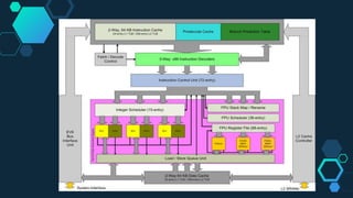


![◇General Architecture
Palomino
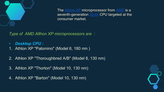
AMD released the third-generation
Athlon, code-named "Palomino", on
October 9, 2001 as the Athlon XP. The
"XP" suffix is interpreted to
mean extended performance and also
as an unofficial reference to
Microsoft Windows XP.[16] The Athlon
XP was marketed using a PR system,
which compared its relative
performance to an Athlon utilizing the
earlier "Thunderbird" core.](https://image.slidesharecdn.com/amdathlon-copy-170726181435/85/Amd-Athlon-Processors-15-320.jpg)
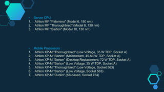
![◇Interestingly, the Palomino core actually debuted
earlier in the mobile market—branded as Mobile Athlon
4 with the codename "Corvette". It distinctively used
a ceramic interposer much like the Thunderbird instead
of the organic pin grid array package used on all later
Palomino processors.[18]](https://image.slidesharecdn.com/amdathlon-copy-170726181435/85/Amd-Athlon-Processors-17-320.jpg)


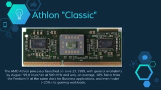
The document discusses the AMD Athlon microprocessor. It describes the original Athlon, also called the Athlon Classic, as the first seventh-generation x86 processor to reach 1 GHz. It then discusses subsequent Athlon models including the Athlon 64, Athlon II, and various Athlon XP processors. Key details are provided on the architectures and specifications of the Thunderbird, Palomino, and other Athlon cores.