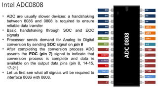
Intel ADC0808
• ADCare usually slower devices: a handshaking
between 8086 and 0808 is required to ensure
reliable data transfer
• Basic handshaking through SOC and EOC
signals
• Processor sends demand for Analog to Digital
conversion by sending SOC signal on pin 6
• After completing the conversion process ADC
asserts the EOC (pin 7) signal to indicate that
conversion process is complete and data is
available on the output data pins (pin 8, 14-15,
17-21)
• Let us first see what all signals will be required to
interface 8086 with 0808.
3.
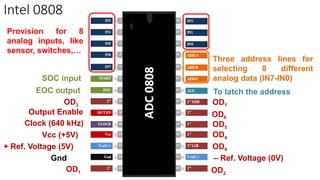
Intel 0808
Provision for8
analog inputs, like
sensor, switches,…
Three address lines for
selecting 8 different
analog data (IN7-IN0)
To latch the address
SOC input
EOC output
Output Enable
Vcc (+5V)
Gnd
+ Ref. Voltage (5V)
– Ref. Voltage (0V)
Clock (640 kHz)
OD3
OD1 OD2
OD0
OD4
OD5
OD6
OD7
4.
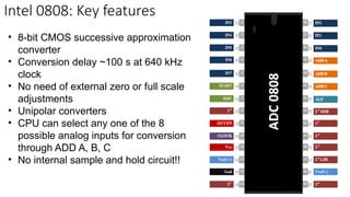
Intel 0808: Keyfeatures
• 8-bit CMOS successive approximation
converter
• Conversion delay ~100 s at 640 kHz
clock
• No need of external zero or full scale
adjustments
• Unipolar converters
• CPU can select any one of the 8
possible analog inputs for conversion
through ADD A, B, C
• No internal sample and hold circuit!!
5.
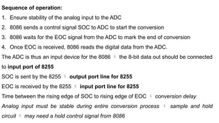
Sequence of operation:
1.Ensure stability of the analog input to the ADC
2. 8086 sends a control signal SOC to ADC to start the conversion
3. 8086 waits for the EOC signal from the ADC to mark the end of conversion
4. Once EOC is received, 8086 reads the digital data from the ADC.
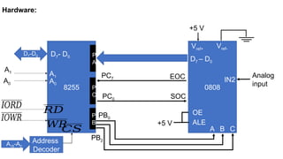
The ADC is thus an input device for the 8086 the 8-bit data out should be connected
to input port of 8255
SOC is sent by the 8255 output port line for 8255
EOC is received by the 8255 input port line for 8255
Time between the rising edge of SOC to rising edge of EOC conversion delay
Analog input must be stable during entire conversion process sample and hold
circuit may need a hold control signal from 8086
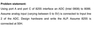
Problem statement:
Using portA and port C of 8255 interface an ADC (Intel 0808) to 8086.
Assume analog input (varying between 0 to 5V) is connected to Input line
2 of the ADC. Design hardware and write the ALP. Assume 8255 is
connected at 50H.
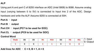
ALP
Using port Aand port C of 8255 interface an ADC (Intel 0808) to 8086. Assume analog
input (varying between 0 to 5V) is connected to Input line 2 of the ADC. Design
hardware and write the ALP. Assume 8255 is connected at 50H.
Port A input
Port B output
Port CH input (PC7 to be used for EOC)
Port CL output (PC0 to be used for SOC)
Control Word
Add lines for ADC C = 0, B = 1, A = 0
Mode D6 D5 PA PCH D2 PB PCL
1 0 0 1 1 0 0 0
1: Input
0: Output
10.
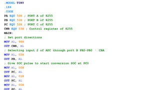
.MODEL TINY
.186
.CODE
PA EQU50H ; PORT A of 8255
PB EQU 51H ; PORT B of 8255
PC EQU 52H ; PORT C of 8255
CWR EQU 53H ; Control register of 8255
MAIN:
; Set port directions
MOV AL, 98H
OUT CWR, AL
; Selecting input 2 of ADC through port B PB2-PB0 CBA
MOV AL, 02H
OUT PB, AL
; Give SOC pulse to start conversion SOC at PC0
MOV AL, 00H
OUT PC, AL
MOV AL, 01H
OUT PC, AL
MOV AL, 00H
11.
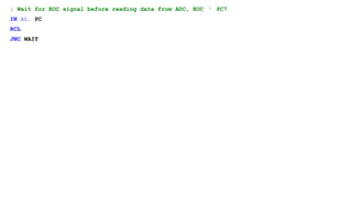
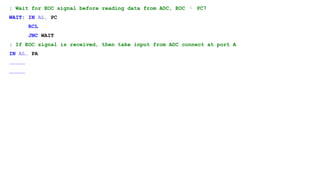
; Wait forEOC signal before reading data from ADC, EOC PC7
IN AL, PC
RCL
JNC WAIT
12.
; Wait forEOC signal before reading data from ADC, EOC PC7
WAIT: IN AL, PC
RCL
JNC WAIT
; If EOC signal is received, then take input from ADC connect at port A
IN AL, PA
……………
……………
13.
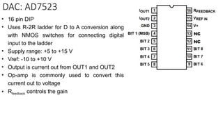
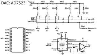
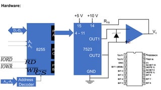
DAC: AD7523
• 16pin DIP
• Uses R-2R ladder for D to A conversion along
with NMOS switches for connecting digital
input to the ladder
• Supply range: +5 to +15 V
• Vref: -10 to +10 V
• Output is current out from OUT1 and OUT2
• Op-amp is commonly used to convert this
current out to voltage
• Rfeedback controls the gain
NC
NC
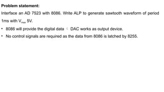
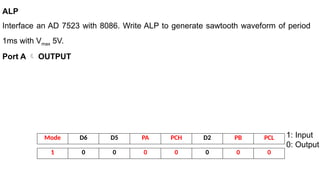
Problem statement:
Interface anAD 7523 with 8086. Write ALP to generate sawtooth waveform of period
1ms with Vmax 5V.
• 8086 will provide the digital data DAC works as output device.
• No control signals are required as the data from 8086 is latched by 8255.
ALP
Interface an AD7523 with 8086. Write ALP to generate sawtooth waveform of period
1ms with Vmax 5V.
Port A OUTPUT
Mode D6 D5 PA PCH D2 PB PCL
1 0 0 0 0 0 0 0
1: Input
0: Output
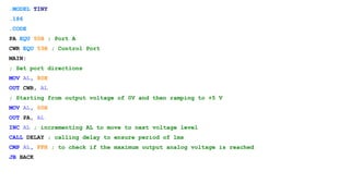
18.
.MODEL TINY
.186
.CODE
PA EQU50H ; Port A
CWR EQU 53H ; Control Port
MAIN:
; Set port directions
MOV AL, 80H
OUT CWR, AL
; Starting from output voltage of 0V and then ramping to +5 V
MOV AL, 00H
OUT PA, AL
INC AL ; incrementing AL to move to next voltage level
CALL DELAY ; calling delay to ensure period of 1ms
CMP AL, FFH ; to check if the maximum output analog voltage is reached
JB BACK
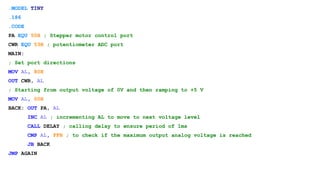
19.
.MODEL TINY
.186
.CODE
PA EQU50H ; Stepper motor control port
CWR EQU 53H ; potentiometer ADC port
MAIN:
; Set port directions
MOV AL, 80H
OUT CWR, AL
; Starting from output voltage of 0V and then ramping to +5 V
MOV AL, 00H
BACK: OUT PA, AL
INC AL ; incrementing AL to move to next voltage level
CALL DELAY ; calling delay to ensure period of 1ms
CMP AL, FFH ; to check if the maximum output analog voltage is reached
JB BACK
JMP AGAIN
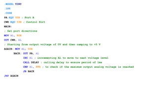
20.
.MODEL TINY
.186
.CODE
PA EQU50H ; Port A
CWR EQU 53H ; Control Port
MAIN:
; Set port directions
MOV AL, 80H
OUT CWR, AL
; Starting from output voltage of 0V and then ramping to +5 V
AGAIN: MOV AL, 00H
BACK: OUT PA, AL
INC AL ; incrementing AL to move to next voltage level
CALL DELAY ; calling delay to ensure period of 1ms
CMP AL, FFH ; to check if the maximum output analog voltage is reached
JB BACK
JMP AGAIN


![Interfacing technique with 8085- ADC[0808]](https://cdn.slidesharecdn.com/ss_thumbnails/adc-160307140900-thumbnail.jpg?width=640&height=640&fit=bounds)