
Recommended
More Related Content
What's hot
What's hot (20)
Similar to Ac lab final_report
Similar to Ac lab final_report (20)
Recently uploaded
Recently uploaded (20)
Ac lab final_report
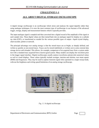
- 1. EC 010 408 Analog Communication Lab Journal Department of Electronics and Communication, MITS, Cochin Page CHALLENGE # -1 ALL ABOUT DIGITAL STORAGE OSCILLOSCOPE A digital storage oscilloscope is an oscilloscope which stores and analyses the signal digitally rather than using analogue techniques. It is now the most common type of oscilloscope in use because of the advanced trigger, storage, display and measurement features which it typically provides. The input analogue signal is sampled and then converted into a digital record of the amplitude of the signal at each sample time. These digital values are then turned back into an analogue signal for display on a cathode ray tube (CRT), or transformed as needed for the various possible types of output—liquid crystal display, chart recorder, plotter or network. The principal advantage over analog storage is that the stored traces are as bright, as sharply defined, and written as quickly as non-stored traces. Traces can be stored indefinitely or written out to some external data storage device and reloaded. This allows, for example, comparison of an acquired trace from a system under test with a standard trace acquired from a known-good system. Many models can display the waveform prior to the trigger signal interface. Digital oscilloscopes usually analyze waveforms and provide numerical values as well as visual displays. These values typically include averages, maxima and minima, root mean square (RMS) and frequencies. They may be used to capture transient signal when operated in a single sweep mode, with-out the brightness and writing speed limitations of an analog storage oscilloscope. Fig. 1.1 A digital oscilloscope
- 2. EC 010 408 Analog Communication Lab Journal Department of Electronics and Communication, MITS, Cochin Page DIGITAL STORAGE OSCILLOSCOPE OBJECTIVE: To study about DSO (Digital Storage Oscilloscope), its features and basic operations. 1.1 OVERVIEW: In this challenge we will come across the features and basic operations of DSO.A digital storage oscilloscope is an oscilloscope which stores and analyses the signal digitally rather than using analogue techniques. It is now the most common type of oscilloscope in use because of the advanced trigger, storage, display and measurement features which it typically provides. Here we will come across the specifications of DSO, become familiar with front panel controls, displaying data. 1.2 SPECIFICATIONS OF DSO: Bandwidth Definition: Bandwidth is defined as a band containing all frequencies between upper cut-off frequency and lower cut-off frequencies. The upper and lower cut-off(3dB)frequencies corresponds to the frequencies where the magnitude of signal’s Fourier Transform is reduced to half (3dB less than) its maximum value. Significance: It enables computation of the power required to transmit a signal. Bandwidth of DSO: 50MHz. Sampling Rate Definition: Sampling rate or sampling frequency defines the number of samples per second (or per other unit) taken from a continuous signal to make a discrete or digital signal. For time-domain signals like the waveforms for sound (and other audio-visual content types), frequencies are measured in hertz (Hz) or cycles per second. Significance: The more samples taken per second, the more accurate the digital representation of the sound can be. For example, the current sample rate for CD-quality audio is 44,100 samples per second. This sample rate can accurately reproduce the audio frequencies up to 20,500 hertz, covering the full range of human hearing. Sampling Rate Of DSO: 1GSa/s Vertical Sensitivity: Turn the large knob above the channel key to set the sensitivity (volts/division) for the channel. The vertical sensitivity knob changes the analog channel sensitivity in a 1-2-5 step sequence (with a 1:1 probe attached). The analog channel Volts/Div value is displayed in the status line. Horizontal range: It is the minimum and maximum horizontal time division.
- 3. EC 010 408 Analog Communication Lab Journal Department of Electronics and Communication, MITS, Cochin Page Accuracy: It is how accurately the DSO works Model Bandwidth Sampling Rate Vertical Sensitivity Horizontal range Accuracy 1052B 50MHz 1GSa/sec 2mV-10V 5ns-50s Time base accuracy: 2mV - 5mV (+-4%) 1.2 GETTING STARTED 1.2.1 Load the default Oscilloscope set up The default configuration returns the oscilloscope to its default settings. This places the oscilloscope in a known operating condition. The major default settings are: Horizontal: main mode, 100μs/div scale, 0 s delay, center time reference. Vertical: Channel 1 on, 5 V/div scale, DC coupling, 0 V position, 1 MΩ impedance, probe factor to 1.0 if an Auto probe is not connected to the channel. Trigger: Edge trigger, Auto sweep mode, 0 V level, channel 1 source, DC coupling, rising edge slope, 60 ns hold-off time. Display: Vectors on, 33% grid intensity, infinite persistence off. Other: Acquire mode normal, Run/Stop to run, cursors and measurements off. 1.2.2 Use Auto Scale Auto scale automatically configures the oscilloscope to best display the input signal by analyzing any waveforms connected to the channel and external trigger inputs. This includes the digital channels on MSO models. Auto scale finds, turns on, and scales any channel with a repetitive waveform that has a frequency of at least 50 Hz, a duty cycle greater than 0.5%, and amplitude of at least 10 mV peak to peak. Any channels that do not meet these requirements are turned off. The trigger source is selected by looking for the first valid waveform starting with external trigger, then continuing with the highest number analog channel down to the lowest number analog channel, and finally (if the oscilloscope is an MSO) the highest number digital channel. During Auto-scale, the delay is set to 0.0 seconds, the sweep speed setting is a function of the input signal (about 2 periods of the triggered signal on the screen), and the triggering mode is set to edge. Vectors remain in the state they were before the Auto-scale. 1.2.3 Become familiar with Front Panel Controls
- 4. EC 010 408 Analog Communication Lab Journal Department of Electronics and Communication, MITS, Cochin Page Figure of front Panel Fig.1.2 DSO front panel a) Entry Knob: The entry knob is used to select items from menus and to change values. Its function changes based upon which menu is displayed. Note that the curved arrow symbol above the entry knob illuminates whenever the entry knob can be used to select a value. Use the entry knob to select among the choices that are shown on the soft keys b) Setup Controls The default setup and auto-scale together constitute the setup control. They are used to change setup and configuration of the waveform. c) File controls Press the File key to access file functions such as save or recall a waveform or setup. Or press the Quick Print key to print the waveform from the display. d) Horizontal controls You can use the horizontal controls to change the horizontal scale and position of waveforms. The horizontal position readout shows the time represented by the centre of the screen, using the time of the trigger as zero. Changing the horizontal scale causes the waveform to expand or contract around the screen centre. e) Run controls Press the Run/Stop to make the oscilloscope begin looking for a trigger. The Run/Stop key will illuminate in green. If the trigger mode is set to “Normal,” the display will not update until a trigger is found. If the trigger mode is set to “Auto,” the oscilloscope looks for a trigger, and if none is found, it will automatically trigger, and the
- 5. EC 010 408 Analog Communication Lab Journal Department of Electronics and Communication, MITS, Cochin Page display will immediately show the input signals. In this case, the background of the Auto indicator at the top of the display will flash, indicating that oscilloscope is forcing triggers. Press the Run/Stop again to stop acquiring data. The key will illuminate in red. Now you can pan across and zoom-in on the acquired data. Press Single to make a single acquisition of data. The key will illuminate in yellow until the oscilloscope triggers. f) Menu controls It includes: 1) CH1 and CH2: Channel 1, channel 2 menu control button. 2) MATH: MATH function control button. 3) REF: Reference waveforms control button. 4) HORI MENU: Horizontal control button. 5) TRIG MENU: Trigger control button. 6) SET TO 50%: Set the trigger level to midpoint of the signal amplitude. 7) FORCE: Use the FORCE button to complete the current waveform acquisition whether the oscilloscope detects a trigger or not. This is useful for Single acquisitions and Normal trigger mode. 8) SAVE/RECALL: Display the Save/Recall Menu for setups and waveforms. 9) ACQUIRE: Display the Acquire Menu. 10) MEASURE: Display the automated measurements menu. 11) CURSORS: Display the Cursor Menu. Vertical Position controls adjust cursor position while displaying the Cursor Menu and the cursors are activated. Cursors remain displayed (unless the Type option is set to Off) after leaving the Cursor Menu but are not adjustable. 12) DISPLAY: Display the Display Menu. 13) UTILITY: Display the Utility Menu. 14) DEFAULT SETUP: Recall the factory setup. 15) HELP: Enter the online help system. 16) AUTO: Automatically sets the oscilloscope controls to produce a usable display of the input signals. 17) RUN/STOP: Continuously acquires waveforms or stops the acquisition. Note:If waveform acquisition is stopped (using the RUN/STOP or SINGLE button), the SEC/DIV control expands or compresses the waveform. 18) SINGLE: Acquire a single waveform and then stops.
- 6. EC 010 408 Analog Communication Lab Journal Department of Electronics and Communication, MITS, Cochin Page g) Trigger Controls These controls determine how the oscilloscope triggers to capture data.The trigger determines when the oscilloscope starts to acquire data and display a waveform. When a trigger is set up properly, the oscilloscope converts unstable displays or blank screens into meaningful waveforms. 1) TRIG MENU Button: Press the TRIG MENU Button to display the Trigger Menu. 2) LEVEL Knob: The LEVEL knob is to set the corresponding signal voltage of trigger point in order to sample. Press the LEVEL knob can set trigger level to zero. 3) SET TO 50% Button: Use the SET TO 50% button to stabilize a waveform quickly. The oscilloscope can set the Trigger Level to be about halfway between the minimum and maximum voltage levels automatically. This is useful when you connect a signal to the EXT TRIG BNC and set the trigger source to Ext or Ext/5. 4) FORCE Button: Use the FORCE button to complete the current waveform acquisition whether the oscilloscope detects a trigger or not. This is useful for SINGLE acquisitions and Normal trigger mode. 5) Pre-trigger/Delayed trigger: The data before and after trigger the trigger position is typically set at the horizontal centre of the screen, in the full-screen display the 6div data of pre trigger and delayed trigger can be surveyed. More data of pre-trigger and 1s delayed trigger can be surveyed by adjusting the horizontal position. h) Vertical Controls Use this knob to change the channel’s vertical position on the display. There is one Vertical Position control for each channel. Use vertical sensitivity knob to change the vertical sensitivity (gain) of the channel i) Soft keys It is used to select between different menu options. j) Front Panel Overlays for different languages The oscilloscopes have twelve languages' user menu to be selected. Press the “Utility” button →“language” to select language. 1.2.4 Become familiar with the oscilloscope display
- 7. EC 010 408 Analog Communication Lab Journal Department of Electronics and Communication, MITS, Cochin Page Fig 1.3 1052B DSO display 1.2.5 Using Run Control keys This is a switch that stops or starts oscilloscope data acquisition. When running, the switch becomes green. When stopped, the switch becomes red and the upper left of the screen displays “STOP”. When the upper left of the screen displays “PLAY, this switch start the waveform play-back. 1.2.6 Access the built in help The built in help can be used for self-guidance. This can be viewed by pressing any switch displayed on the oscilloscope for 2-3sec. 1.3 DISPLAYING DATA 1.3.1 Using the Horizontal Controls a) Horizontal scale Adjust the horizontal position of all channels and math waveforms (the position of the trigger relative to the centre of the screen). The resolution of this control varies with the time base setting. b) Horizontal Position When you press the horizontal POSITION Knob, you can set the horizontal position to zero. c) Zoomed time base Y-T: We get the zoomed version of a segment of the signal. X-Y: In this mode we get the transfer characteristics of the signal. 1.3.2 Using the vertical Controls
- 8. EC 010 408 Analog Communication Lab Journal Department of Electronics and Communication, MITS, Cochin Page a) Vertical Scale Vertical scale is used to scale the amplitude of the signal. It gives the volt/div. b) Vertical position Vertical position can give the value at any point vertically. c) Channel Coupling d) Bandwidth The range of frequencies an oscilloscope can usefully display is referred to as its bandwidth. Bandwidth applies primarily to the Y-axis, although the X-axis sweeps have to be fast enough to show the highest- frequency waveforms. The bandwidth is defined as the frequency at which the sensitivity is 0.707 of that at DC or the lowest AC frequency (a drop of 3 dB). The oscilloscope's response will drop off rapidly as the input frequency is raised above that point. e) Probe Attenuation To minimize loading, attenuator probes (e.g., 10X probes) are used. A typical probe uses a 9 mega ohm series resistor shunted by a low-value capacitor to make an RC compensated divider with the cable capacitance and scope input. The RC time constants are adjusted to match. f) Digital Filter g) Volts/div control sensitivity This is used to control the volts/div. h) Invert waveform This helps to invert our original waveform. 1.3.3 Using Math function a) Add To perform the addition of channel 1 and channel 2, select Invert in the Channel 2 menu and perform the 1 + 2 math function. Press the Math key, press the 1 + 2 soft-key, then press the Settings soft-key if you want to change the scaling or offset for the subtract function. Scale — lets you set your own vertical scale factors for subtract, expressed as V/div (Volts/division) or A/div (Amps/division). Units are set in the channel Probe menu. Press the Scale soft-key, then turn the Entry knob to rescale 1 + 2.
- 9. EC 010 408 Analog Communication Lab Journal Department of Electronics and Communication, MITS, Cochin Page Offset— lets you set your own offset for the 1 + 2 math function. The offset value is in Volts or Amps and is represented by the center horizontal grid line of the display. Press the Offset soft-key, and then turn the Entry knob to change the offset for 1 + 2. b) Subtract When you select 1 – 2, channel 2 voltage values are subtracted from channel 1 voltage values point by point, and the result is displayed. You can use 1 – 2 to make a differential measurement or to compare two waveforms. You may need to use a true differential probe if your waveforms have DC offsets larger than dynamic range of the oscilloscope's input channel. To perform the subtraction of channel 1 and channel 2, select Invert in the Channel 2 menu and perform the 1 – 2 math function. Press the Math key, press the 1 – 2 soft-key, then press the Settings soft-key if you want to change the scaling or offset for the subtract function. Scale — lets you set your own vertical scale factors for subtract, expressed as V/div (Volts/division) or A/div (Amps/division). Units are set in the channel Probe menu. Press the Scale soft-key, then turn the Entry knob to rescale 1 – 2. Offset — lets you set your own offset for the 1 – 2 math function. The offset value is in Volts or Amps and is represented by the center horizontal grid line of the display. Press the Offset soft-key, and then turn the Entry knob to change the offset for 1 – 2. c) Multiply When you select 1 * 2, channel 1 and channel 2 voltage values are multiplied point by point, and the result is displayed. 1 * 2 is useful for seeing power relationships when one of the channels is proportional to the current. 1 Press the Math key, press the 1 * 2 soft-key, then press the Settings soft-key if you want to change the scaling or offset for the multiply function. Scale — lets you set your own vertical scale factors for multiply expressed as /div (Volts- squared/division), /div (Amps-squared/division), or W/div (Watts/division or Volt-Amps/division). Units are set in the channel Probe menu. Press the Scale soft-key, then turn the Entry knob to rescale 1 * 2. Offset — lets you set your own offset for the multiply math function. The offset value is in V2 (Volts- squared), / (Amps-squared), or W (Watts) and is represented by the center horizontal grid line of the display. Press the Offset soft-key, and then turn the Entry knob to change the offset for 1 * 2. d) FFT
- 10. EC 010 408 Analog Communication Lab Journal Department of Electronics and Communication, MITS, Cochin Page FFT is used to compute the fast Fourier transform using analog input channels or math functions 1 + 2, 1 – 2, or 1 * 2. FFT takes the digitized time record of the specified source and transforms it to the frequency domain. When the FFT function is selected, the FFT spectrum is plotted on the oscilloscope display as magnitude in d BV versus frequency. The readout for the horizontal axis changes from time to frequency (Hertz) and the vertical readout changes from volts to dB. Use the FFT function to find crosstalk problems, to find distortion problems in analog waveforms caused by amplifier non-linearity, or for adjusting analog filters. Press the Math key, press the FFT soft-key, then press the Settings soft-key to display the FFT menu. Source — selects the source for the FFT. The source can be any analog channel, or math functions 1 + 2, 1 – 2, and 1 * 2. Span — sets the overall width of the FFT spectrum that you see on the display (left to right). Divide span by 10 to calculate the number of Hertz per division. It is possible to set Span above the maximum available frequency, in which case the displayed spectrum will not take up the whole screen. Press the Span soft-key, and then turn the Entry knob to set the desired frequency span of the display. 1.4 MAKING MEASUREMENTS 1.4.1 Displaying Automatic Measurements The following automatic measurements can be made in the Meas. menu. 1) Time Measurements • Counter • Duty Cycle • Frequency • Period • Rise Time • Fall Time • + Width • – Width • X at Max • X at Min 2) Phase and Delay • Phase • Delay 3) Voltage Measurements • Average • Amplitude • Base
- 11. EC 010 408 Analog Communication Lab Journal Department of Electronics and Communication, MITS, Cochin Page • Maximum • Minimum • Peak-to-Peak • RMS • Std. Deviation • Top 4) Pre-shoot and Overshoot • Pre-shoot • Over-shoot 1.4.2 Voltage Measurements Measurement units for each input channel can be set to Volts or Amps using the channel Probe Units soft key. A scale unit of U (undefined) will be displayed for math function 1-2 and for d/dt, and ∫ dt when 1-2 or 1+2 is the selected source if channel 1 and channel 2 are set to dissimilar units in the channel Probe Units soft key. 1.4.3 Time Measurements 1) Counter The oscilloscopes have an integrated hardware frequency counter which counts the number of cycles that occur within a period of time (known as the gate time) to measure the frequency of a signal. The gate time for the Counter measurement is automatically adjusted to be 100 ms or twice the current time window, whichever is longer, up to 1 second. The Counter can measure frequencies up to the bandwidth of the oscilloscope. The minimum frequency supported is 1/(2 * gate time). The measured frequency is normally displayed in 5 digits, but can be displayed in 8 digits when an external 10 MHz frequency reference is provided at the 10 MHz REF rear panel BNC and gate time is 1 second (50 ms/div sweep speed or greater). The hardware counter uses the trigger comparator output. Therefore, the counted channel’s trigger level (or threshold for digital channels) must be set correctly. The Y cursor shows the threshold level used in the measurement. Any channel except Math can be selected as the source. Only one Counter measurement can be displayed at a time.
- 12. EC 010 408 Analog Communication Lab Journal Department of Electronics and Communication, MITS, Cochin Page Fig 1.4 2) Duty Cycle The duty cycle of a repetitive pulse train is the ratio of the positive pulse width to the period, expressed as a percentage. The X cursors show the time period being measured. The Y cursor shows the middle threshold point. Digital channel time measurements, Automatic time measurements Delay, Fall Time, Phase, Rise Time, X at Max, and X at Min, and are not valid for digital channels on mixed-signal oscilloscopes. Duty cycle = 3) Period Period is the time period of the complete waveform cycle. The time is measured between the middle threshold points of two consecutive, like-polarity edges. A middle threshold crossing must also travel through the lower and upper threshold levels which eliminates runt pulses. The X cursors show what portion of the waveform is being measured. The Y cursor shows the middle threshold point. 4) Fall Time The fall time of a signal is the time difference between the crossing of the upper threshold and the crossing of the lower threshold for a negative-going edge. The X cursor shows the edge being measured. For maximum measurement accuracy, set the sweep speed as fast as possible while leaving the complete falling edge of the waveform on the display. The Y cursors show the lower and upper threshold points. 5) Rise Time
- 13. EC 010 408 Analog Communication Lab Journal Department of Electronics and Communication, MITS, Cochin Page The rise time of a signal is the time difference between the crossing of the lower threshold and the crossing of the upper threshold for a positive-going edge. The X cursor shows the edge being measured. For maximum measurement accuracy, set the sweep speed as fast as possible while leaving the complete rising edge of the waveform on the display. The Y cursors show the lower and upper threshold points. 6) + Width + Width is the time from the middle threshold of the rising edge to the middle threshold of the next falling edge. The X cursors show the pulse being measured. The Y cursor shows the middle threshold point. 7) – Width – Width is the time from the middle threshold of the falling edge to the middle threshold of the next rising edge. The X cursors show the pulse being measured. The Y cursor shows the middle threshold point. 1.4.4 Making cursor Measurements You can use the cursors to make custom voltage or time measurements on oscilloscope signals, and timing measurements on digital channels. 1) Connect a signal to the oscilloscope and obtain a stable display. 2) Press the Cursors key. View the cursor functions in the soft-key menu: 3) Mode: Set the cursor to measure voltage and time (Normal), or display the binary or hexadecimal logic value of the displayed waveforms. 4) Source — selects a channel or math function for the cursor measurements. 5) X Y — Select either the X cursors or the Y cursors for adjustment with the Entry knob. 6) X1 and X2 — adjust horizontally and normally measure time. 7) Y1 and Y2 — adjust vertically and normally measure voltage. 8) 1 X2 and Y1 Y2 — move the cursors together when turning the Entry knob. CONCLUSION The study about digital oscilloscope was competed. They are small portable with high band width. It provides colour displays, on screen measurements, storage, printing and PC connectivity.
- 14. EC 010 408 Analog Communication Lab Journal Department of Electronics and Communication, MITS, Cochin Page CHALLENGE# 1 AM RADIO STATION About the challenge: AM broad casting is a process of radio broadcasting using AM. A unidirectional wireless transmission of signals over radio waves intended to reach a wide audience is done here. The signal types can be either analog or digital. AM radio can be broadcasted on several f bands: Long wave = 153 to 279K Hz Medium wave = 526.5 to 1606 KHz Short wave = 2.3 to 26.1 MHz The standard AM broadcast band is 530 to 1700 kHz. Band was expanded in 1990s by adding 5 channels. Channels are spaced every 9 KHZ everywhere. T he advantage of AM is that its signal can be detected with simple equipments. AM receiver detects amplitude variations in radio waves at a particular frequency. I t then is amplified to drive a loudspeaker. There is low audio quality in AM broadcasting due to audio bandwidth limit. And thereby defining the objectives, Objective 1: Audio signal generation The audio signal is picked up using a microphone and the electrical audio output is then filtered and amplified using an Op-amp Amplifier circuit. Objective 2: Amplitude Modulation Prior to transmission the message signal is modulated with a high frequency carrier signal using amplitude modulation scheme. Different electronic circuits can be designed for implementing AM Modulation. a) Collector Modulation using Class C Circuit b) Emitter Modulation using Class A Circuit c) Using Op-amp d) Using AD633
- 15. EC 010 408 Analog Communication Lab Journal Department of Electronics and Communication, MITS, Cochin Page Objective 3: AM Radio Receiver A simple AM radio Receiver make needs just a few elements: a) LC tank circuit which is a tuning arrangement (unless one station happens to be overwhelmingly stronger than all the others; not likely); b) Demodulator: a way to “demodulate” the signal: that is, to detect the information that is broadcast, peeling it away from the uninteresting “carrier,” a higher-frequency oscillation that is used to help the information to travel c) Amplifier: a way to let this relatively-feeble signal do enough work to make a signal audible to you (the earliest and simplest radios used no amplifier at all; but we need one, because we listen with conventional “low impedance” headphones, of the sort used with a walkman or diskman: these won’t work with a feeble source.
- 16. EC 010 408 Analog Communication Lab Journal Department of Electronics and Communication, MITS, Cochin Page OBJECTIVE 1: Audio Signal Generation: The audio signal is to be picked up using a microphone and the electrical audio output need to be filtered and then amplified using an Op-amp Amplifier circuit. PRELAB ACTIVITIES INTRODUCTION An audio frequency (abbreviation: AF) or audible frequency is characterized as a periodic vibration whose frequency is audible to the average human. The SI unit of audio frequency is the hertz (Hz). It is the property of sound that most determines pitch. Audio-frequency signal generators generate signals in the audio-frequency range and above. Applications include checking frequency response of audio equipment, and many uses in the electronic laboratory. Equipment distortion can be measured using a very-low-distortion audio generator as the signal source, with appropriate equipment to measure output distortion harmonic-by-harmonic with a wave analyzer, or simply total harmonic distortion. A distortion of 0.0001% can be achieved by an audio signal generator with a relatively simple circuit. The generally accepted standard range of audible frequencies is 20 to 20,000 Hz, although the range of frequencies individuals hear is greatly influenced by environmental factors. Frequencies below 20 Hz are generally felt rather than heard, assuming the amplitude of the vibration is great enough. Frequencies above 20,000 Hz can sometimes be sensed by young people. The microphone is a transducer —in other words, an energy converter. It senses acoustic energy (sound) and translates it into equivalent electrical energy. Amplified and sent to a loudspeaker or headphone, the sound picked up by the microphone transducer should emerge from the speaker transducer with no significant changes. Condenser (or capacitor) microphones use a lightweight membrane and a fixed plate that act as opposite sides of a capacitor. Sound pressure against this thin polymer film causes it to move. This movement changes the capacitance of the circuit, creating a changing electrical output. Condenser microphones are preferred for their very uniform frequency response and ability to respond with clarity to transient sounds. The low mass of the membrane diaphragm permits extended high-frequency response, while the nature of the design also ensures outstanding low-frequency pickup. They weigh much less than dynamic elements and they can be much smaller. Using microphone we can receive the audio signal and send it to op amp to amplify the signal. The microphone act like a sound controlled variable resistor. That sound wave that microphone picks up control the resistance of microphone. The changing resistance causes the voltage on microphone’s ungrounded pin to change according to amplitude of sound wave on microphones. This produces audio frequency AC voltage signal at microphone’s ungrounded pin. The audio-signal then passes through the large capacitor to block all DC voltages and is amplified using inverting amplifier circuit.
- 17. EC 010 408 Analog Communication Lab Journal Department of Electronics and Communication, MITS, Cochin Page THOUGHT EXPERIMENT “TO PICK UP AUDIO SIGNAL USING CONDENSER MICROPHONE AND AMPLIFY IT” Our aim is to pick the message signal and amplify it using op amp. So send message signal to microphone. For the working of microphone a bias voltage is given and in order to control the flow of current through microphone a current limiting resistor is need to connect between microphone and DC source. We needs to pick up the audio signal and get back amplified signal. Since op-amp provides high gain, feed the audio signal picked up using microphone to op-amp and we will get amplified signal back. Since we need to amplify an audio signal, ie, only a band of frequencies in between, we design a BP, ie, a combination of HPF with cutoff frequency 20 Hz and LPF with cutoff frequency 20KHz. The capacitor at the beginning of BPF blocks any DC content form the microphone bias voltage penetrating into the filter circuit. To amplify the picked up signal, we opt for an op-amp with a desired gain of 10.Op amp are chosen since they are excellent voltage amplifiers. Positive feedback provides oscillation which is not appreciated here. So we go for negative feedback here. Depending on whether the feedback is given at inverting or non inverting terminal of op-amp, the gain- feedback resistor relation varies. For an inverting amplifier, the relation is A=Rf/R. DESIGN: The condenser microphone needs a small DC current to make it operate correctly. This current is controlled by R3.Specification of condenser microphone is Maximum operating voltage = 1O V and current consumption is0.8mA The voltage across capacitor in microphone varies above or below bias voltage. Since maximum operating voltage is 10V. Let bias voltage be 9 V. Current limiting resistor R3 is R3 = = 11.2 KΩ The audio frequency range is 20 Hz to 20 KHz. We need to design a BPF. So the signal ranging in this frequency gets amplified by op-amp ie, to avoid noises.
- 18. EC 010 408 Analog Communication Lab Journal Department of Electronics and Communication, MITS, Cochin Page The lowest frequency that need to amplified be 20 Hz ie, For HPF, fc= = 20 Hz Let C= 10 µF R= = 1KΩ The highest frequency, ie cut-off frequency of LPF is 20 KHz Let C =10nF R= = 796.18Ω (standard 1KΩ) Let gain of op amp be 10 ie, 10= let R1= 1KΩ ie R2= 10 KΩ DESIGN OF MICROPHONE CIRCUIT From datasheet, Rin input impedance of the condenser microphone is 1.8KΩ Maximum current through microphone is 0.8mA Maximum bias voltage of the microphone is 10V Here we take bias voltage as 8V R = = 10KΩ For the capacitor, C = = as R = 1KΩ, so C = 15µF CIRCUIT
- 19. EC 010 408 Analog Communication Lab Journal Department of Electronics and Communication, MITS, Cochin Page
- 20. EC 010 408 Analog Communication Lab Journal Department of Electronics and Communication, MITS, Cochin Page FREQUENCY RESPONSE OF BPF OUTPUT OF BPF AT 1 KHz and 10 VPP
- 21. EC 010 408 Analog Communication Lab Journal Department of Electronics and Communication, MITS, Cochin Page Final output COMPONENTS REQUIRED SL NO COMPONENT VALUES QUALITY 1 resistor 11.2KΩ, 10KΩ, 1KΩ 1 2 capacitor 10nF, 10µF 1 3 Condenser microphone - 1 4 Op-amp AD741 1 5 DC power supply - 1 6 DSO - 1 7 breadboard - 1
- 22. EC 010 408 Analog Communication Lab Journal Department of Electronics and Communication, MITS, Cochin Page INLAB ACTIVITIES: PROCEDURE 1. Setup the BPF as per the diagram 2. Give input using function generator and output using DSO 3. Observe the output for various input frequencies 4. Draw frequency verses gain graph 5. Now complete the circuit as per the diagram 6. Observe output waveform for different input frequencies 7. Calculate gain OBSERVATION: Checking operation of op-amp alone, Vin = 12.8mVpp gives Vo=130mVpp Thus the gain is 130/12.8=10.1. With the whole circuit, VIN= 9.2mVPP Sl. No. Frequency (Hz) Vo(Vmax) (m) Gain in dB (20log vo/vin) 1 10 5.6 -4.31 2 20 6 -3.71 3 40 6.8 -2.62 4 100 7.5 -1.77 5 500 8.5 -.68 6 1K 8.7 -.485 7 2K 9 -.19 8 5K 9 -.19 9 10K 8.4 -.79 10 15K 7.8 -1.43 11 20K 6.6 -2.88 12 25 K 6.2 -3.42 13 30 K 5.4 -4.6 14 40K 5.2 -4.95
- 23. EC 010 408 Analog Communication Lab Journal Department of Electronics and Communication, MITS, Cochin Page GRAPH Bandwidth = 24.9 KHz POSTLAB ACTIVITIES DISCUSSION: Designed cut off frequency was 20Hz and 20 KHz ie, our audio frequency range. Practically the cut off frequency that we got was 30 Hz and 20KHz.ie, bandwidth = 25 K – 20 = 24.976 KHz Inverting amplifier which is designed at gain 10 gives a gain 10.1.While keeping amplifier and BPF together the output gain get reduced due to the effect of BPF on op amp. Microphone has 2 ends. The one with 3 ends is negative. The circuit output increased as frequency increased and then reduced. RESULT: An audio signal generator was designed. Designed cut off frequency of HPF = 20 Hz Observed cut off frequency of HPF = 30 Hz
- 24. EC 010 408 Analog Communication Lab Journal Department of Electronics and Communication, MITS, Cochin Page Designed cut off frequency of LPF = 20 KHz Observed cut off frequency of LPF = 20 KHz The frequency response of BPF was plotted and the bandwidth was found to be 27.976 KHz
- 25. EC 010 408 Analog Communication Lab Journal Department of Electronics and Communication, MITS, Cochin Page DATA SHEET
- 26. EC 010 408 Analog Communication Lab Journal Department of Electronics and Communication, MITS, Cochin Page
- 27. EC 010 408 Analog Communication Lab Journal Department of Electronics and Communication, MITS, Cochin Page
- 28. EC 010 408 Analog Communication Lab Journal Department of Electronics and Communication, MITS, Cochin Page
- 29. EC 010 408 Analog Communication Lab Journal Department of Electronics and Communication, MITS, Cochin Page Objective 2: Amplitude Modulation: Prior to transmission the message signal is modulated with a high frequency carrier signal using amplitude modulation scheme. Different electronic circuits can be designed for implementing AM Modulation. a) Emitter Modulation using Class A Circuit b) Collector Modulation using Class C Circuit c) Using Op amp d) Using AD633
- 30. EC 010 408 Analog Communication Lab Journal Department of Electronics and Communication, MITS, Cochin Page OBJECTIVE 2(a): To design an am Emitter Modulation using Class A Circuit and to perform detailed study on the circuits behaviour for various inputs, changes in modulation index and to determine the modulation index using XY view. PRELAB ACTIVITIES: INTRODUCTION Modulation is the process of changing characteristics of a carrier wave with respect to a modulating wave. This modulating wave is otherwise known as the message signal which has the information to be transmitted. For example in amplitude modulation the amplitude of the carrier signal is varied in accordance with modulating signal. Amplitude modulation more popularly known in its abbreviated form as AM, is a method of communication used mostly in the form of radio waves. Weaker signals can be heard over stronger, closer ones with AM, allowing for emergency transmission to have more chance of being heard over other traffic. Also AM uses a narrower band width than FM, allowing more users in a small space. This is important for the lower frequencies of radio, where space is at a premium. There are two levels of modulation, low level modulation and high level modulation. In low level modulation the modulation take place prior to the output element of the final stage of transmitter. In high level modulators the modulation takes place in the final element of the final stage of transmitter.
- 31. EC 010 408 Analog Communication Lab Journal Department of Electronics and Communication, MITS, Cochin Page Low level AM modulator When no modulating signal is present, the circuit operates a linear amplifier, the output is simply the carrier amplified by voltage again. When a modulating signal is applied, the amplifier operates non-linearly and signal multiplication occurs. Av = AC[1 + m(t)sin 2πfmt] ,Av = AQ [1± M] ,AVMAX = 2Aq ,AVMIN =0 Av → amplifier voltage gain with modulation AQ → amplifier quiescent (with modulation) voltage gain Modulation signal is applied through isolation transformer to the emitter of transistor and the carrier is applied directly to the base. The modulating signal drives the circuit in to both saturation and cut-off states, producing non-linear amplification necessary for modulation to occur. The collector waveform includes the carrier, upper and lower side frequencies as well as a component at the modulating frequency. Coupling capacitor C2, removes the modulating signal frequency from the waveform, producing a symmetrical AM envelop at VOUT. We fix the Q point of circuit in the midpoint. Midpoint biasing allows optimum or best AC operation of amplifier. When an AC signal is applied to base of transistor, IC and VCC vary around Q point. When Q point is centred, IC and VCC can both make maximum possible transistors above or below initial DC values. When
- 32. EC 010 408 Analog Communication Lab Journal Department of Electronics and Communication, MITS, Cochin Page Q point is above centre on load line, input may cause transistor to saturation and a part of output sinusoidal wave will clipped off. Similarly Q point below centred will also cause cut off. CE configuration in h parameter is voltage amplifier. Stability factor of a transistor is defined as the ratio of amount of change in collector current to the amount of change in the same collector current with the base open. Lesser the stability factor, that type of biasing is more desired. The stability factor of voltage divider bias is nearly equal to one. THOUGHT EXPERIMENT We need to design AM modulator using class A amplifier. Characteristics of Class A are: 1) Amplitude of the output signal depends on the amplitude of input carrier and the voltage gain of the amplifier. 2) Coefficient of modulation depends entirely on the amplitude of modulating signal. 3) Simple but is capable of producing high-power output waveforms. The carrier signal is given to the base terminal of transistor and message is given to the emitter terminal. We use high frequency transistor BF195, BC107 can also be used because it is found to be working in the frequency range up to 1MHz. Class A amplifier RC coupled Amplifier. The output coupling capacitor and load will act as a filter. We need to design load and capacitor using filter characteristics. The final output should be a modulated wave. DESIGN Let, VCC = 12 V, ICQ = 2 mA, VCE = 0.5VCC = 6, VE = 0.1VCC = 1.2V, VC = 0.6VCC =7.2V VE = IE RE; RE = VE / IE = 1.2/2*10-2 = 600Ω ≈ 680Ω VB = VBE + IE RE = 0.7+1.2 = 1.9V We have; (hfe +1) RE ≤ 10R2 R2 = (hfe +1) RE / 10 = (111*600) /10 = 6.3KΩ RC = (VCC - VC) /IC = (12-7.2) / (2*10-2 ) = 2.4KΩ ≈ 2.7KΩ VB = (VCC R2) / (R1+R2) R1 = (12R2 – 1.9R2) / 1.9 = 35KΩ ≈ 33kΩ Design of capacitors, XCIN ≤ Zin/10 hie = (hfe VT)/(ICQ) = 1430
- 33. EC 010 408 Analog Communication Lab Journal Department of Electronics and Communication, MITS, Cochin Page Zin = R1||R2||hie = 2.2KΩ, Cin = 1/(2π XCINf) = 15µF XCE ≤ RE /10 RE =680Ω, CE = 1/(2πXCEf) ≈ 100µ XCOUT ≤ RC /10, COUT = 1/(2π XCOUTf) = 6.6µF Design of load resistor, AVO = (AVRL) /(RC+RL) ,We have; AV = (hfeRC)/hie = 18.615 Let AVO=100 = 18.615RL / (RC+RL); RL = 3.3KΩ Designed circuit, Because of too many non- linearity in the modulated signal, we have to redesign the output capacitor .We consider the output as a high pass filter with cut off frequency 500KHz ,which is the frequency of the carrier. fC = 500 KHz ,RL = 3.3 KΩ ,FC = 1/(2πRC); C = 100Pf Re-designed circuit diagram,
- 34. EC 010 408 Analog Communication Lab Journal Department of Electronics and Communication, MITS, Cochin Page Working, When an amplifier is biased in such that it always operates in the linear region where the output is an amplified version of input signal, it is a class A amplifier. In this, Q point is fixed in the active region. It delivers maximum power to the load. Only 25% of power absorbed from dc source is delivered to the load. That is, 75% is stored in amplifiers resistors and transistors. Here the message signal is applied in the emitter and hence it is known as emitter modulator. The carrier signal is applied to the base of the transistor. Two signal generators are used in the circuit. One is for representing a high frequency carrier signal and other representing low frequency message signal. The two signals are mixed and amplified by the transistors. Hence class A acts as a modulator. COMPONENTS REQUIRED SI.NO COMPONENT SPECIFICATION QUANTITY 1 Resistor 3.3kΩ,680Ω,6.8kΩ,33kΩ,2.4kΩ 1 2 Capacitor 100pF,100µF,15µF 1 3 Transistor BF195 1 4 Function generator 30Hz-3MHz 2 5 D C power supply 0-30V 1 6 Oscilloscope - 1 7 Bread board - 1
- 35. EC 010 408 Analog Communication Lab Journal Department of Electronics and Communication, MITS, Cochin Page PROCEDURE 1. Make connection as shown in the circuit diagram 2. Feed the message and carrier signal. Connect the output of the circuit to CRO 3. Observe the range of message frequency and carrier frequency over which the AM modulator gives the best result and calculate the µ value 4. Observe the value of µfor µ˃1by increasing the amplitude of message signal , which leads to over modulation and also for µ<1 ,which leads to under modulation 5. Picture the Oscilloscope in XY view and note the value of µwith time domain 6. Observe the frequency domain result and sketch SIMULATION
- 36. EC 010 408 Analog Communication Lab Journal Department of Electronics and Communication, MITS, Cochin Page INLAB ACTIVITIES OBSERVATIONS Without message signal, VIN = 9mv, VOUT = 458mv, AV=458/9=50.88 FC=500khz,fm=2khz ,Am=109mv VMAX=25.6mv, VMIN=13.6m V, µ=(25.6-13.6)/(25.6+13.6)=.3 Range of best results, fc - 1k to 2.5KHz ,fm - 450 to 520KHz ,AC = 90 to 120mv ,AM=16 to 30mv
- 37. EC 010 408 Analog Communication Lab Journal Department of Electronics and Communication, MITS, Cochin Page GRAPH
- 38. EC 010 408 Analog Communication Lab Journal Department of Electronics and Communication, MITS, Cochin Page
- 39. EC 010 408 Analog Communication Lab Journal Department of Electronics and Communication, MITS, Cochin Page
- 40. EC 010 408 Analog Communication Lab Journal Department of Electronics and Communication, MITS, Cochin Page
- 41. EC 010 408 Analog Communication Lab Journal Department of Electronics and Communication, MITS, Cochin Page
- 42. EC 010 408 Analog Communication Lab Journal Department of Electronics and Communication, MITS, Cochin Page POSTLAB ACTIVITIES DISCUSSION The output of the coupling capacitor and the load passes all the harmonics with initially designed ones. So, consider it as an HPF with cut off frequency not much less than fc – fm will give a linear output. So the circuit have to be modified like that. As m(t) varies from sine to ramp, amplitude of modulated also varies implies that envelope of modulated signal clearly depends on the m(t) .At times, when modulated wave is not obtained, using a 10K port and varying it might give an modulated output. The Am must be larger than Ac here, because, the Am here is modulating the amplified carrier signal. RESULT An AM modulator using a class A amplifier was designed.AM modulation for different message signals were observed and it was found that there was a difference in the theoretical and practical modulation indices. 1. For a sine input as message, µ = 0.3 2. For square input as message, µ = 0.34 3. For triangle input, µ = 0.34 4. For sum of sinusoids, µ = 0.28 This difference took place due to the fact that theoretically we assume that the system is ideal. But practically it is not an ideal system.
- 43. EC 010 408 Analog Communication Lab Journal Department of Electronics and Communication, MITS, Cochin Page
- 44. EC 010 408 Analog Communication Lab Journal Department of Electronics and Communication, MITS, Cochin Page OBJECTIVE 2(b): To design an AM Collector Modulation using Class C Circuit and to perform detailed study on the circuits behaviour for various inputs, changes in modulation index and to determine the modulation index using XY view. PRE LAB ACTIVITY INTRODUCTION In electronics and communication modulation is the process of varying one or more properties of a periodic wave form, called the carrier signal with a modulating signal that typically contains information to be transmitted. The sinusoidal signal that is used in modulation is known as carrier signal or simply carrier and the signal used in modulating the carrier signal is known as message signal. This carrier wave is usually a much higher frequency than the input signal. Class C amplifier is a type of amplifier where the active element conduct for less than one half cycles means the conduction angle is less than 180 degree. The reduced conduction angle improves the efficiency to a great extend but causes a lot of distortion. Theoretical maximum efficiency of a class c is above 90%. Due to huge amount of distortion, class c is not used in audio applications. The most common application of class c includes radio frequency circuits like RF oscillator, RF amplifier etc. In class c amplifier am modulator design the audio frequency transistor is used since the message signal frequency is in AF range and intermediate frequency transistor is used to suppress the harmonics and to pass the fundamental frequency. THOUGHT EXPERIMENT Amplitude modulation can be achieved by using devices which have nonlinear input-output characteristics, like exponential relationships. A diode is another nonlinear device, having an exponential relation between input and output. Apart from all of these, the nonlinear behaviour can be achieved in a more controlled manner by varying the biasing of a BJT, preferably in an amplifier circuit. When taking BJT as a possible solution to the design problem any class of amplifier can be used. But there comes the issue of power consumption by the amplifier circuit. Taking this aspect into account a class C operation would give the necessary non-linearity while at the same time significantly reducing the power consumed. The carrier is given as the input signal by applying to the base of the BJT using a capacitive coupling. Since the frequency of the input is high, a BJT capable of high frequency operation is to be used. So instead of medium frequency transistor BC107, a high frequency operating transistor BF195 is used. A resistance of high value is connected across the base-emitter junction so as to keep the time period of the capacitor discharging very high. As a result, the capacitor will charge quickly, via the capacitor-base-emitter loop (which will essentially be a very low resistance path), but discharges very slowly via the capacitor- resistor loop as its time constant is designed to be very high. The capacitor now acts almost like a constant voltage source, shifting the base voltage e level so as to drive the transistor to Class C operation.
- 45. EC 010 408 Analog Communication Lab Journal Department of Electronics and Communication, MITS, Cochin Page The modulating signal is applied at the collector via transformer coupling i.e, using an Audio Frequency Transformer (since the message signal has a frequency which is in the AF range).A tank circuit is also connected in series between the collector terminal and the message signal. It can be regarded as a highly selective i.e. high quality filter that suppresses the harmonics in class C waveform and passes its fundamental frequency. The tank circuit is incorporated in the circuit by using an Intermediate Frequency Transformer (IFT). The tank circuit together with the amplifier constitute a tuned amplifier. The resonant frequency of the tank circuit is set to be the frequency of the carrier signal. The output at the collector terminal of the BJT is a series of current pulses with their amplitudes proportional to the modulating signal. The current pulses initiates damped oscillations in the tuned circuit. The train of pulses fed to the tank circuit would generate a series of complete sine waves proportional in amplitude to the size of the pulses. Thus we get an amplitude modulated signal at output of the tank. The class C amplifier has very high efficiency and is used in high frequency. So it provides high power which required for amplitude modulated signal generation. DESIGN A resistance of high value is connected across the base-emitter junction so as to keep the time period of the capacitor discharging very high. The time constant is designed to be very high. Let time constant t=0.1s, T=RC Let R= 1MΩ, C=t/R = 0.1/106 , C= 0.1µF CIRCUIT DIAGRAM
- 46. EC 010 408 Analog Communication Lab Journal Department of Electronics and Communication, MITS, Cochin Page COMPONENTS REQUIRED: SL NO. COMPONENTS SPECIFICATIONS QUANTITY 1 High frequency BJT BF195 1 2 High value resistor 1MΩ 1 3 Capacitor 0.1µF 1 4 Audio frequency transformer - 1 5 Intermediate frequency transformer IF=455KHz 1 INLAB ACTIVITIES PROCEDURE 1. Sketch the time domain results with sinusoid message. 2. Modify the system to obtain a modulating index equal to and greater than 1 (i.e., greater than 100%), and sketch the resulting signal. 3. Find the range of message frequency and carrier frequency over which the AM modulator gives the best results. 4. Picture the Oscilloscope in XY view when X plates of the CRO is fed with modulating tone and Y plates with AM signal a. μ can be calculated as μ= − / + 5. Use the FFT capability of your scope to obtain the Frequency Domain display. Sketch the Frequency Domain results. OBSERVATIONS After tuning IFT to give maximum gain at 455 KHz, With AC = 8.34 V pp and fC =455 KHZ Am = 5 VPP and fm= 2 KHZ, modulation occurred at: VMAX =5.2 V, VMIN=3V, Theoretical µ =AM / AC = .599 Practically µ= (VMAX- VMIN) / (VMAX + VMIN) = .268 Frequency range of message signal in which modulation occurs is 500 HZ – 10 KHZ Amplitude range of message signal is 3 V pp – 10 V pp
- 47. EC 010 408 Analog Communication Lab Journal Department of Electronics and Communication, MITS, Cochin Page POST LAB ACTIVITIES: GRAPH
- 48. EC 010 408 Analog Communication Lab Journal Department of Electronics and Communication, MITS, Cochin Page DISCUSSION Properly modulated wave is obtained only when the message f is of range 500Hz to 10 KHz. Fig: over modulated waveform Fast Fourier Transform will allow the frequency content of a signal to be displayed along with the amplitude of various frequency components. Distortion caused by non-linear operation of analog circuitry can be easily shown by using FFT analysis. The amplitude of the spectrum can be observed in linear or dB V (RMS) scale. For class C modulation, the maximum amplitude is observed at the carrier frequency, fc= 455kHz Intermediate frequency transformers come as specially designed tuned circuits in ground-able metal packages called IF cans. The primary winding has an inductance of Leq=450 µH and it comes with a shunt capacitor of capacitance C = 270pF. Its resonant frequency is thus, f = = 455 KHz. The frequency is adjustable by a factor of ±10 percent. IFT has a tapped primary winding. The ferrite core between the primary and the secondary winding is tuned with a non-metallic screw driver or tuning tool. It changes the mutual inductance and thus controlling the Q-factor of the collector circuit of connected transistor. Out of the three pins at the input, middle pin should be connected to the power supply and the other one to the collector of the transistor and the two pins on another side to the output respectively. AFT works at frequencies between about 20Hz- 20 KHz and are used in audio frequency amplifier circuits. The turn ratio of AFT is 1:1. The primary of AFT is connected to the message signal and the secondary to the power supply as well as to IFT. The transistor used in class C amplifier is BF195, which is a high frequency transistor. The left-most terminal is collector and the right most terminal is emitter and the middle-one is base. BF194/195 is a high frequency transistor with the following characteristics.
- 49. EC 010 408 Analog Communication Lab Journal Department of Electronics and Communication, MITS, Cochin Page RESULT AM modulator circuit using class c amplifier was designed and the modulated wave was observed. The practical and theoretical index varied by 0.599.268=.331. Over modulation was obtained when the amplitude of message signal was made to increase.
- 50. EC 010 408 Analog Communication Lab Journal Department of Electronics and Communication, MITS, Cochin Page
- 51. EC 010 408 Analog Communication Lab Journal Department of Electronics and Communication, MITS, Cochin Page OBJECTIVE 2(c): To design an AM Modulation using Op-amp and to perform detailed study on the circuits behaviour for various inputs, changes in modulation index and to determine the modulation index using XY view. PRELAB ACTIVITY INTRODUCTION Here, FET is used as a variable resistor and op-amp is used as a non inverting amplifier for the carrier signal. For op-amp, Rf act as feedback resistor and the resistance of an N- channel junction FET act as a input resistance Rl, the gain of the circuit is given by A = 1 + In the absence of modulating signal FET provides a fixed resistance and therefore the gain of the non inverting amplifier is constant, giving steady carrier output on the application of modulating signal the resistance of FET will vary. A positive going s modulating input signal will cause the FET resistance to decrease, whereas a negative going modulating signal will cause it to increase. Increasing the FET resistance cause op-amp circuit gain to increase and vice-versa. This results in an AM signal at the output of the op- amp. THOUGHT EXPERIMENT Our aim is to design an AM modulator using op-amp .The role of FET is to act as a variable resistor .In the absence of modulating signal FET provides a fixed resistance .By the application of modulating signal FET resistance varies thus gain starts to increase and decrease depending on the FET resistance. Thus we get an amplitude modulated signal. DESIGN Higher value resistors are not precise so it wouldn’t give us precise gain and lower value resistors sink higher current from source. There are downfalls with choosing very large and small resistors. These usually deal with non ideal behaviour of components or other requirements such as power and heat. Small resistors means we need a much higher current to provide voltage drops for op-amp to work .Most op-amps are able to provide 10’s of m A’s. Even if op-amp can provide many amperes there will be lot of heat generated in resistors which may be problematic. On the other hand large resistor runs into problems dealing with non ideal behaviour of op-amp terminals. So value of Rf is chosen in midrange (10K-100K) So therefore assume Rf = 10K
- 52. EC 010 408 Analog Communication Lab Journal Department of Electronics and Communication, MITS, Cochin Page CIRCUIT DIAGRAM SIMULATION Message signal m(t) Carrier signal c(t) Modulated signal (Output)
- 53. EC 010 408 Analog Communication Lab Journal Department of Electronics and Communication, MITS, Cochin Page COMPONENTS REQUIRED SL NO COMPONENTS SPECIFICATION QUANTITY 1 Op-amp µA741 1 2 Resistor 10KΩ 1 3 J-FET BFW10 1 4 DC Power supply ±15V 1 IN LAB ACTIVITY: OBSERVATIONS Range where the best results were obtained, Fm = 120Hz to 30 KHz, fC = 485KHz to 495KH z AM = 1.1mV to 109 m V, AC - .11 V to .12 V With AM =109mv, Ac=110mv, fC=490KHz ,fm=5KHz Theoretically, mod index=1, practically index = (-360—600)/(-360-600)= .25
- 54. EC 010 408 Analog Communication Lab Journal Department of Electronics and Communication, MITS, Cochin Page GRAPH
- 55. EC 010 408 Analog Communication Lab Journal Department of Electronics and Communication, MITS, Cochin Page POSTLAB ACTIVITY: DISCUSSION An AM Modulator using op-amp is basically a low level modulator. The modulation index of the circuit was observed to be 0.257. When Amplitude of message signal is made to increase over modulation occurs which results in loss of information of the AM wave. The shield terminal of JFET has no connection here. It is used to sink the temperature of JFET. For an n-channel JFET, negative voltage has to be given at the gate. This is called negative off- setting. But, since this JFET has a capacity range of -400Mv to +140Mv and we don’t give m(t) greater than +140Mv ,it doesn’t affect output even if we give positive voltage at gate. RESULT AM circuit using op amp was designed and the output was observed. Theoretical value of modulation index (µ) = 0.14 Practically obtained modulation index (µ) = 0.257 Over modulation was obtained when the amplitude of message signal was made to increase.
- 56. EC 010 408 Analog Communication Lab Journal Department of Electronics and Communication, MITS, Cochin Page
- 57. EC 010 408 Analog Communication Lab Journal Department of Electronics and Communication, MITS, Cochin Page OBJECTIVE 2(d): To design an AM Modulation using AD633 IC and to perform detailed study on the circuits behaviour for various inputs, changes in modulation index and to determine the modulation index using XY view. PRE LAB ACTIVITY INTRODUCTION An analog multiplier IC AD633 (Analog Devices) has been used to generate the AM signal. The AD633 is a functionally complete, four-quadrant, analog multiplier. Four quadrant means that both operands that are multiplied can take any polarity i.e, +/- and hence multiplication can happen across four quadrants. It includes high impedance, differential X and Y inputs, and a high impedance summing input (Z). AD 633 is well suited for applications such as modulation, demodulation, automatic gain control, power measurement, voltage controlled amplifier etc. The inputs range of operating voltage for this IC is from +15V to -15V. So while designing this circuit keep in mind that inputs do not exceed this limit. The low impedance output voltage is a nominal 10 V full scale provided by a buried Zener. The functional diagram of the AD633 is shown in Figure. The AD633 can be used as a linear amplitude modulator with no external components. The carrier and modulation inputs to the AD633 are multiplied to produce a double sideband signal. The carrier signal is fed forward to the Z input of the AD633 where it is summed with the double sideband signal to produce a double sideband with the carrier output. THOUGHT EXPERIMENT We use AD633 for amplitude modulation for a large number of reasons like 1) Most simplest and efficient method of modulation technique. 2) Provides high efficiency. 3) Promises carrier suppression. Here there is no need for external components so we need not design them. DESIGN
- 58. EC 010 408 Analog Communication Lab Journal Department of Electronics and Communication, MITS, Cochin Page Provide the supply voltage of +15 V to pin 8 of the IC and -15 V to pin 5 of the IC. To the Y and Z inputs of the IC, feed the carrier sinusoid of amplitude Ac = 4V and frequency fc = 50 kHz. To the X input of the IC, feed the message sinusoid of amplitude Am = 3 V and frequency fm = 1 kHz. SIMULATIONS
- 59. EC 010 408 Analog Communication Lab Journal Department of Electronics and Communication, MITS, Cochin Page COMPONENTS REQUIRED SL NO. COMPONENTS SPECIFICATION QUANTITY 1 IC AD633 1 2 DC Power supply ±15V 1 INLAB ACTIVITIES OBSERVATIONS Carrier Message Theoretical µ =0.6 Practical µ From X-Y view,
- 60. EC 010 408 Analog Communication Lab Journal Department of Electronics and Communication, MITS, Cochin Page B=3.76V A=1.04V µ =0.56
- 61. EC 010 408 Analog Communication Lab Journal Department of Electronics and Communication, MITS, Cochin Page GRAPH
- 62. EC 010 408 Analog Communication Lab Journal Department of Electronics and Communication, MITS, Cochin Page POSTLAB ACTIVITIES DISCUSSION The circuit is simple. We obtain modulated wave easily. The message signal is given to the 1st and 2nd pin. The carrier is given to the 3rd and 4th pin. are given to the 8th and 5th pin respectively which must not exceed +-15V. The output is taken across the 7th pin. The modulation index µ is calculated and over- modulation was observed. RESULT The AM modulation using AD633 was designed and the output was observed and µ is calculated. µ= µ= 0.2 From transfer characteristic µ=0.56
- 63. EC 010 408 Analog Communication Lab Journal Department of Electronics and Communication, MITS, Cochin Page
- 64. EC 010 408 Analog Communication Lab Journal Department of Electronics and Communication, MITS, Cochin Page OBJECTIVE 3:To design an AM detector circuit using a tuned LC circuit and an envelope detector circuit in order to obtain the output signal having same frequency and amplified amplitude as that of the message signal. PRE-LAB ACTIVITY INTRODUCTION Detector is used at the receiving section to demodulate the signal received so that proper message signal can be retrieved. A simple AM demodulator is a diode envelope detector. It can be implemented by a simple diode envelope detector to eliminate the negative half of the carrier envelope followed by a simple RC filter to remove the high frequency carrier. The result will be the low frequency envelope which is the demodulated message. A point contact diode with low junction capacitance is used in the circuit as it is has to rectify high frequency carrier. It offers low impedance at high frequency. The RC elements connected after the diode acts as a filter. It acts as a low-pass filter which eliminates high frequency carrier at the same time it retains the low frequency message signal. Thus the output of the filter contains the low frequency modulating signal with a dc offset. The dc offset voltage is proportional to the strength of the modulated signal received by the receiver in a transmission reception system, which in turn is proportional to the strength (amplitude) of the carrier. In the case of commercial AM radio receiver, detectors are placed after the intermediate amplifier stage. The carrier at this section is tuned to a frequency of 455 kHz respectively. Since the ripple content is 100 times higher than that of the highest base band signal and will not pass through any subsequent audio amplifier. A tuner is a subsystem that receives RF transmission and converts the selected carrier and its associated bandwidth into a fixed frequency suitable for further processing. The first stage includes simple tuner circuit, which selects a frequency of many available frequencies, parallel LC is used for this purpose. The next stage is an envelope detector. The diode in this detector works as an HWR, which is followed by a LPF. THOUGHT EXPERIMENT The first stage of the circuit is a tuner circuit that will tunes the circuit to a particular frequency. Radio stations mainly broadcast for the frequency 500 kHz- 1MHz. when the value of the capacitor and inductor are equal, resonance will be observed. A particular frequency is picked up by the circuit when the inductor resistance increase with increase in frequency and the capacitive reactance decreases with decrease in frequency. Detector circuit mainly consists of diode which is tuned as a high pass filter followed by low pass filter. Amplifier stage is also designed in order to get back the audible signal. DESIGN
- 65. EC 010 408 Analog Communication Lab Journal Department of Electronics and Communication, MITS, Cochin Page The simplest demodulator circuit includes a transmitted AM wave, a LC circuit, germanium diode and a LPF. As due to shortage of availability of the inductor we design an inductor by calculating the windings and obtain frequency response TUNER CIRCUIT Let us assume that the broadcasting frequency as 500 kHz. For an tuned LC circuit, f = Assume capacitance value as 2nF, where for LC circuit L = L = 50µH For winding the inductor, L = 4π2 r2 nN*10-9 Where, n= N / l Let length =1.5 cm Where N = loops n = turns per cm r = radius of square bobbin The square bobbin is of side length - 1:1cm r = r = 0.564 cm Hence, L = 4π2 r2 N*10-9 N2 = π N = 75.56
- 66. EC 010 408 Analog Communication Lab Journal Department of Electronics and Communication, MITS, Cochin Page N = 76 turns ENVELOPE DETECTOR For proper discharging, Where carrier frequency fc = 500 kHz and the message frequency, fm = 5 kHz Hence capacitance, C = 0.02µF Where, 100Ω So that resistor value is, R = 1.8kΩ AMPLIFIER Assume the gain of the non-inverting amplifier as 10 AV = 1+ Let us assume R1 to be 1kΩ Therefore, Rf = 9kΩ CIRCUIT AND SIMULATION
- 67. EC 010 408 Analog Communication Lab Journal Department of Electronics and Communication, MITS, Cochin Page Using diode only
- 68. EC 010 408 Analog Communication Lab Journal Department of Electronics and Communication, MITS, Cochin Page Full circuit Q1 BC107BP R1 33kΩ R2 6.8kΩ R3 680Ω R4 2.7kΩ R5 3.3kΩ R6 1.8kΩ R7 10kΩ C1 100pF C2 100µF C3 2nF C5 0.02µF L1 50µH XFG1 D1 DIODE_VIRTUAL U1 741 3 2 4 7 6 51 R8 10kΩ VCC 12V VEE -12V C4 10µF XFG2
- 69. EC 010 408 Analog Communication Lab Journal Department of Electronics and Communication, MITS, Cochin Page
- 70. EC 010 408 Analog Communication Lab Journal Department of Electronics and Communication, MITS, Cochin Page IN LAB ACTIVITY OBSERVATIONS OF MODULATED OUTPUT
- 71. EC 010 408 Analog Communication Lab Journal Department of Electronics and Communication, MITS, Cochin Page OBSERVATIONS OF DEMODULATOR Output from demodulator So VMAX = 130mV At the function generator, for message signal VMAX = 101mV, fm = 1 KHz. For carrier signal, V peak-peak = .53V, fc = 450 KHz. Output from op-amp -2 -1.5 -1 -0.5 0 0.5 1 1.5 2 0 2 4 6 8 10 12 14 16 18 voltage(mV) time message signal -2 -1.5 -1 -0.5 0 0.5 1 1.5 2 0 2 4 6 8 10 12 14 16 18 voltage(V) time message signal
- 72. EC 010 408 Analog Communication Lab Journal Department of Electronics and Communication, MITS, Cochin Page So VMAX = 1.38v At the function generator, message signal, VMAX = 101mV and fM = 1 KHz So for carrier signal, VMAX = .53V, fC = 450 KHz. Now as observed from the output is VPP = 2.76V Now, gain = So that, gain = = 13.67 Now assumed the gain = 10. For LC circuit The input voltage is 1V (peak to peak) Frequency (Hz) Output Voltage (V) Gain (Vo/Vin) 3 Hz 42 mV -27.53 50 Hz 70 mV -23.09 100 Hz 70 mV -23.09 600 Hz 70 mV -23.09 1 KHz 80 mV -21.93 5 KHz 80 mV -21.93 10 KHz 100 mV -20 20 KHz 120 mV -13.07 50 KHz 280 mV -11.05 100 KHz 520 mV -5.67 300 KHz 840 mV -1.514 500 KHz 1.01 V 0.86 600 KHz 1V 0 1 MHz 800 mV -1.93
- 73. EC 010 408 Analog Communication Lab Journal Department of Electronics and Communication, MITS, Cochin Page POST LAB ACTIVITIES DISCUSSION 1) The detector was performed from the output of class A modulator. The output was obtained by replacing load resistor with port 2) The tuned circuit was not placed in the circuit, since tuned LC circuit require an antenna. The modulated wave is directly fed into the diode. 3) The frequency response of the tuned circuit has to be observed where it gives maximum gain. The point of maximum gain must be carrier frequency only then it passes fC components to diode. 4) The output from op-amp must be sine wave with frequency of same message signal and amplified output. RESULT An AM demodulator was designed and a sinusoidal signal with frequency same as that of message signal was amplified. The frequency response of tank circuit was observed. The amplitude of amplified signal = 2.76V. The amplitude of demodulated signal = 130mV. The amplitude of the output across diode 0A79 is 640mV. -30 -25 -20 -15 -10 -5 0 5 10 100 1000 10000 100000 1000000 gain in dB frequency(KHz) tank circuit response
- 74. EC 010 408 Analog Communication Lab Journal Department of Electronics and Communication, MITS, Cochin Page It is observed that the maximum gain is obtained for frequency 500 KHz. The designed theoretical frequency is 500 KHz.
- 75. EC 010 408 Analog Communication Lab Journal Department of Electronics and Communication, MITS, Cochin Page CHALLENGE # 2 SUPER HETERODYNE RECEIVER OBJECTIVE: To study about super heterodyne receiver PROBLEM Radio receivers are electronic device that receives radio waves and converts the information to a useful form. Radio waves have frequencies from 3 THz to as low as 3 KHz. Radio waves are transmitted by radio transmitters and received by radio receivers. The basic requirement for any communications receiver is to have the ability to select a signal of desired frequency, while rejecting closely adjacent frequencies (Selectivity) and provide sufficient amplification to recover the modulating signal (Sensitivity). A receiver with good selectivity will isolate the desired signal in the RF spectrum and eliminate all other signals. Early radio receivers consisted of one or a number of tuned radio frequency stages with individual tuned circuits which provided the selectivity to separate one received signal from the others. TRF system is a straightforward concept at high frequencies it becomes difficult to build, is less efficient, has small gain and suffers bandwidth changes. Since all its RF stages function at the same frequency, stray coupling between output and input circuits may provide sufficient feedback to cause instability or oscillation. Furthermore, it is difficult to achieve uniform amplification of the RF stages over the entire frequency range of the receiver. At the higher frequencies, the gain of each stage tends to fall off and, therefore, the sensitivity of the receiver is reduced. Finally, the most serious drawback of the TRF receiver is that the selectivity of the tuned circuits cannot be kept uniform over the frequency range. At the high-frequency end of the tuning range, the selectivity of the TRF receiver decreases markedly. This lack of selectivity can become serious at the higher frequencies generally used in electronic communication systems. The bandwidth of a tuned circuit of given Q is directly proportional to its operational frequency and hence, as higher and higher operating frequencies came into use, it became more difficult to achieve sufficient selectivity using the TRF receiver system. SCIENCE AND ENGINEERING The super heterodyne radio or to give it its full name the super heterodyne receiver is one of the most popular forms of receiver in use today in a variety of applications from broadcast receivers to two way radio communications links as well as many mobile radio communications systems. Although other forms of radio receiver are used, the super heterodyne receiver is one of the most widely used forms. Although initially developed in the early days of radio, or wireless technology, the super heterodyne
- 76. EC 010 408 Analog Communication Lab Journal Department of Electronics and Communication, MITS, Cochin Page receiver offers significant advantages in many applications. Naturally the basic concept has been developed since its early days, and more complicated and sophisticated versions are used, but the basic concept still remains the same. Heterodyne is to mix 2 frequencies together, in a non-linear device or to translate one frequency to another. It consist of RF Amplifier Mixer IF Amplifier Envelope Detector Audio Amplifier Fig 1: block diagram of super heterodyne The incoming signal can be mixed with a frequency to produce sum and difference frequency components. The lower frequency difference component called the intermediate frequency (IF), is separated from the other components by fixed tuned amplifier stages set to the intermediate frequency. The non-linearity is necessary to provide the mathematical equivalent of time multiplication between the LO voltage and the RF signal voltage. A tuned circuit at the Mixer output selects the Difference frequency (i.e. the IF or Intermediate frequency). The LO frequency is tunable over a wide range and therefore the Mixer can translate a wide range of input frequencies to the IF.
- 77. EC 010 408 Analog Communication Lab Journal Department of Electronics and Communication, MITS, Cochin Page The output of the mixer is amplified by one or more IF amplifier stages. Most of the receiver sensitivity and selectivity is to be found in these stages. All IF stages are fixed and tuned to only (this standard is fixed at 455 KHz). Hence, high selectivity can be obtained. The highly amplified IF signal is now applied to the detector or demodulator where the original modulating signal is recovered. The detector output is then amplified to drive a Loudspeaker. This requires learning about oscillating circuits, amplifiers, and band pass filters. DETAILED This can be achieved using tuned LC circuits resonating at the desired frequency. LC circuits with a high Q value have narrower bandwidths and hence have better selectivity. However it must be noted the bandwidth must be sufficiently large such that it passes the carrier as well as the sidebands to avoid attenuation and hence distortion of the transmitted information. The sensitivity of a communications receiver is a function of the overall receiver gain. In general, higher gain means better the sensitivity. When an amplitude-modulated (AM) signal is transmitted, it has a certain frequency corresponding to the frequency of the carrier wave. This frequency is combined with a frequency produced in an oscillating circuit in the mixer, which “beats” the two frequencies together. Effectively, the circuit multiplies the two input voltages. By multiplying the two input voltages, the outputs are the sum of the two input frequencies and the difference (known as beating the two frequencies). This “beating” of an incoming signal with a signal produced by an oscillator is what characterizes a super-heterodyne receiver. Choice of intermediate frequency Choosing a suitable intermediate frequency is a matter of compromise. The lower the IF used, the easier it is to achieve a narrow bandwidth to obtain good selectivity in the receiver and the greater the IF stage gain. On the other hand, the higher the IF, the further removed is the image frequency from the signal frequency and hence the better the image rejection. The choice of IF is also affected by the selectivity of the RF end of the receiver. If the receiver has a number of RF stages, it is better able to reject an image signal close to the signal frequency and hence a lower IF channel can be tolerated. Another factor to be considered is the maximum operating frequency the receiver. Assuming Q to be reasonably constant, bandwidth of a tuned circuit is directly proportional to its resonant frequency and hence, the receiver has its widest RF bandwidth and poorest image rejection at the highest frequency end of its tuning range. Use of the fixed lower IF channel gives the following advantages: For a given Q factor in the tuned circuits, the bandwidth is lower making it easier to achieve the required selectivity. At lower frequencies, circuit losses are often lower allowing higher Q factors to be achieved and hence, even greater selectivity and higher gain in the tuned circuits.
- 78. EC 010 408 Analog Communication Lab Journal Department of Electronics and Communication, MITS, Cochin Page It is easier to control, or shape, the bandwidth characteristic at one fixed frequency. Filters can be easily designed with a desired band pass characteristic and slope characteristic, an impossible task for circuits which tune over a range of frequencies. Since the receiver selectivity and most of the receiver pre-detection gain, are both controlled by the fixed IF stages, the selectivity and gain of the super-heterodyne receiver are more consistent over its tuning range than in the TRF receiver. A number of further factors influence the choice of the intermediate frequency: The frequency should be free from radio interference. Standard intermediate frequencies have been established and these are kept dear of signal channel allocation. If possible, one of these standard frequencies should be used. An intermediate frequency which is close to some part of the tuning range of the receiver is avoided as this leads to instability when the receiver is tuned near the frequency of the IF channel. Ideally, low order harmonics of the intermediate frequency (particularly second and third order) should not fall within the tuning range of the receiver. This requirement cannot always be achieved resulting in possible heterodyne whistles at certain spots within the tuning range. Sometimes, quite a high intermediate frequency is chosen because the channel must pass very wide band signals such as those modulated by 5 MHz video used in television. In this case the wide bandwidth circuits are difficult to achieve unless quite high frequencies are used. Standard intermediate frequencies Various Intermediate frequencies have been standardized over the years. In the early days of the super- heterodyne, 175 kHz was used for broadcast receivers in the USA and Australia. These receivers were notorious for their heterodyne whistles caused by images of broadcast stations other than the one tuned. The 175 kHz IF was soon overtaken by a 465 kHz allocation which gave better image response. Another compromise of 262 KHz between 175 and 465 was also used to a lesser extent. The 465 KHz was eventually changed to 455 KHz, still in use today. In Europe, long wave broadcasting took place within the band of 150 to 350 KHz and a more suitable IF of 110 KHz was utilized for this band. The IF of 455 kHz is standard for broadcast receivers including many communication receivers. Generally speaking, it leads to poor image response when used above 10MHz. One commonly used IF for shortwave receivers is 1.600 MHz and this gives a much improved image response for the HF spectrum. An IF standard for VHF FM broadcast receivers is 10.7MHz. In this case, the FM deviation used is 75 kHz and audio range is 15 kHz. The higher IF is very suitable as the wide bandwidth is easily obtained with good
- 79. EC 010 408 Analog Communication Lab Journal Department of Electronics and Communication, MITS, Cochin Page image rejection. A less common IF is 4.300 MHz believed to have been used in receivers tuning the lower end of the VHF spectrum. Multiple conversion Super-heterodyne In receivers tuning the upper HF and the VHF bands, two(or even more) IF channels are commonly used with two (or more) stages of frequency conversion. The lowest frequency IF channel provides the selectivity or bandwidth control that is needed and the highest frequency IF channel is used to achieve good image rejection. The idea behind a super-heterodyne receiver was first hypothesized by Canadian Reginald Fessenden in 1900, but heterodyne reception remained impractical because of the inability to produce a stable signal. The idea was revisited in 1918 by Major Edwin Armstrong of the U.S. Army in France during the First World War. The output of the mixer is amplified by one or more IF amplifier stages. Most of the receiver sensitivity and selectivity is to be found in these stages. All IF stages are fixed and tuned to only (this standard is fixed at 455 KHz). Hence, high selectivity can be obtained. The highly amplified IF signal is now applied to the detector or demodulator where the original modulating signal is recovered. The detector output is then amplified to drive a Loudspeaker. HYPOTHESIS A suitable local oscillator tuning, ganged to the tuning of the signal circuit or radio frequency (RF) stages such that the difference intermediate frequency is always the same fixed value. Detection can then take place at intermediate frequency instead of at radio frequency as in the TRF receiver. EXPERIMENTS TO TEST HYPOTHESIS Design a system to convert incoming signal to intermediate frequency. Design a system that is tuned to intermediate frequency and provide sufficient gain to signal. Design a system to overcome the difficulties of fading in communication channel.
- 80. EC 010 408 Analog Communication Lab Journal Department of Electronics and Communication, MITS, Cochin Page EXPERIMENT 1: Design a system to convert incoming signal to intermediate frequency. PRELAB ACTIVITIES PROBLEM The advantages of super-heterodyne receiver are many. An obvious advantage is that by reducing the incoming frequency to lower intermediate frequency, lower frequency components can be used, and in general, cost is proportional to frequency. Further advantage in that many components can be designed for a fixed frequency (and even shared between different receiver designs), which is easier and cheaper than designing wideband components. To develop a system that change the existing frequency components in the circuit to feed the altered intermediate frequency value (455 KHz for AM Receivers) is the problem. SCIENCE AND ENGINEERING To begin with, a mixer circuit, when considered as a black box, will have two input terminals and one output terminal. One input would correspond to a signal of some frequency that is existing in the circuit whereas the other input would correspond to a local oscillator that is designed to generate a definite frequency value tailor made for the required output frequency. So the designer will have the liberty of deciding at which frequency the oscillator should work so as to get the required output provided the mathematical model of the mixer block is known. The mixer is then a non-linear resistance having two sets of input and one set of output terminals. All mixer circuits make use of the fact that when two sinusoidal signals are multiplied together the resultant consists of sum and difference frequency components. This can be demonstrated as below: If we have two frequencies signal say, Then the signal obtained on multiplying these two signals is
- 81. EC 010 408 Analog Communication Lab Journal Department of Electronics and Communication, MITS, Cochin Page We are usually interested in the term containing the frequency ω1 - ω2 and that is usually the frequency which is filtered out. This frequency is also usually desired to be located in the Intermediate Frequency (IF) as it is required for various applications. For an ideal mixing neither of the two initial input frequencies are present in the output, only the sum and difference frequencies will be present. Now, to produce such a multiplication effect of sinusoidal signals as described above, we can use the non-linearity in the output characteristics of devices such as the BJT. The voltage/current relationship for the transistor is Where IC is the collector current (usually taken as the output current), IS is the reverse saturation current, VBE is the base emitter voltage and VT the thermal voltage. The collector current equation written above can be factored into a dc bias term and a periodic term Or generalizing, Where Now, since is a periodic function it can be expanded into a Fourier series as below
- 82. EC 010 408 Analog Communication Lab Journal Department of Electronics and Communication, MITS, Cochin Page Where the Fourier coefficients In(b) are also modified Bessel functions. Here I0(b) can be regarded as the bias current of the amplifier circuit. If I0(b) is stabilized then Let Now The IC IQ characteristic is given below. With increasing input drive, the current waveform becomes more and more peaky and the peak value can be exceeds the DC bias by a large factor. Now if we can plot the rates of harmonic frequencies to the dc coefficient current against b, ie. Vi VT , We get the curve below:
- 83. EC 010 408 Analog Communication Lab Journal Department of Electronics and Communication, MITS, Cochin Page All the above equations, shows that the BJT output spectrum is rich in harmonics. Again, the exponential can be approximated to the first three terms of its expansion. That is, we model the BJT as having a second order I-V characteristic As a general case, Now, if we make the VBE voltage as the sum or difference of the two signals of different frequencies which are given as inputs, the VBE voltage becomes Substituting this VBE in the output/input equation
- 84. EC 010 408 Analog Communication Lab Journal Department of Electronics and Communication, MITS, Cochin Page Since the RF input applied will be small, the circuits response to it will be linear (or weakly non-linear). But the oscillator input is substantial and it varies the operating point of the circuit periodically. So the overall response to the RF input is a linear-time varying one. Where g(t) is the trans-conductance. The trans-conductance varies periodically and can be expanded in a Fourier series. ωo −→ frequency of local oscillator. When Is applied Hence we get, This again shows that the output of a mixer has various harmonics of the sum and difference frequencies. From the above equation we see that a lot of other frequencies are present at the output which needs to be filtered out by providing a suitable tuned circuit at the output. The output frequency is decided by our needs whether we need a higher frequency than the reference frequency input frequency or a smaller frequency than the reference. Accordingly we select the sum or difference term and filter it out. Fine tuning of the local oscillator over which we have some control. While connecting the oscillator stage and the RF mixer stage the loading issues have to be taken care of. Otherwise there is a possibility of the local oscillators output not being fed to the input of the mixer. This is fine tuning done during circuit assembly. This is the basic mathematical foundation for designing a mixer circuit.
- 85. EC 010 408 Analog Communication Lab Journal Department of Electronics and Communication, MITS, Cochin Page HYPOTHESIS An intuitive way of implementation of a system that converts incoming radio frequency to intermediate frequency would be to utilize the non-linear nature of any three-terminal device(such as BJT) to generate the harmonics of the difference frequencies which could be suitably filtered to get the required frequencies. VARIABLES Independent Variables Input RF voltage Input RF frequency DC power supply Tuned Frequency of IFT Dependent Variables Local Oscillator voltage Local Oscillator frequency Output voltage Output frequency Voltage gain of output signal DESIGN To avoid the case of loading problem, we have to give a substantial amount of resistance at the emitter. The local oscillator output is fed from BE [base emitter] region. The input frequency will be given to the base of the transistor so that EB voltage will be difference of 2 voltages. There has to be a resistance from collector to base biasing. At the output in order to filter out the required output frequency an IFT is kept. Assume VCC = 9v From data sheet of BF 195, ICQ = 4mA, β = 60, VCE = 5v IB = = = 66.6µA By applying KVL, VCC = VCE + [β+1] IBRB So RE = = 1K
- 86. EC 010 408 Analog Communication Lab Journal Department of Electronics and Communication, MITS, Cochin Page For BF 195 VBE = 0.95 VCC = IBRB + VBE + IERE = 9-66.6µA*RB - .95 – (61)*(66.6µA) So equating the terms RB = 64.5K Standard value = 62K The circuit will be as below The capacitors used for coupling are 0.1uF each. This is the design for the circuit. The difference frequency if it falls in the IF range will be altered out by the IFT and observed as a sinusoid at VO. While doing the experiment a variable resistor needs to be kept at the emitter to properly give the output impedance for the oscillator and to ensure that the oscillations are properly coupled to the emitter. The oscillator circuit used is given below:
- 87. EC 010 408 Analog Communication Lab Journal Department of Electronics and Communication, MITS, Cochin Page COMPONENTS REQUIRED SL NO COMPONENTS 1 BF195 1 2 62k resistor 1 3 1k resistor 1 4 10k potentiometer 1 5 IFT 1 6 0.1uF capacitor 2
- 88. EC 010 408 Analog Communication Lab Journal Department of Electronics and Communication, MITS, Cochin Page INLAB ACTIVITIES OBSERVATIONS The carrier frequency, fc = 455 KHz Amplitude, VPP = 0.2V At the output voltage Vpp= 1.42V Frequency, f = 455 KHz FREQUENCY (KHz) OUTPUT VOLTAGE (VOPP) AV = 20log (dB) 400K 120mV -4.436 410K 140mv -3.095 450K 660mV 10.37 452K 800mV 12.041 454K 1.1V 14.80 457K 1.2V 15.563 470K 600mV 9.54 500K 160mV -1.93 OBSERVATION FOR HIGH BEAT VS [V] FLO [Hz] fS [Hz] FIF [Hz]
- 89. EC 010 408 Analog Communication Lab Journal Department of Electronics and Communication, MITS, Cochin Page 2.56 555K 100K 481K 2.72 355K 100K 442K 2.4 755K 300K 455K 2.48 1M 545K 455K 2.4 1.4M 995K 455K 2.24 2M 1.54M 455K OBSERVATION FOR LOW BEAT Vs [V] FLO [Hz] fs [Hz] FIF [Hz] 2.36 300K 755K 455K 2.72 155K 300K 455K 2.56 100K 555K 455K 1.92 2M 3M 455K
- 90. EC 010 408 Analog Communication Lab Journal Department of Electronics and Communication, MITS, Cochin Page GRAPH POSTLAB ACTIVITIES DISCUSSION The frequency response without connecting local oscillator is obtained to check whether the IFT give maximum gain at 455 KHz. Initially local oscillator was not given and the output voltage and frequency was obtained. In high beat injection frequency of the local oscillator is set that it is higher than input frequency. Here as the difference between local oscillator and input voltage become 455 KHz and output voltage increases. In case of low beat injection, frequency of local oscillator is set such that it is lower than input signal frequency. Tuning of IFT Our requirement is to tune IFT to 455 KHz, which is IF frequency. Initially LO was not given and output was obtained. Then IFT is tuned to 455 KHz. After connecting LO the output frequency may not be 455K. So a port of 10K is used at its output and is varied to reach 455 KHz. RESULT Hypothesis was verified. IFT was tuned to 455 KHz with maximum gain. -10 -5 0 5 10 15 20 1 10 100 1000 gain in dB frequency (KHz) frequency response of the mixer
- 91. EC 010 408 Analog Communication Lab Journal Department of Electronics and Communication, MITS, Cochin Page The input frequency is mixed with fL-fS or fL+ fS to be 455 KHz as per high or low beat injection.
- 92. EC 010 408 Analog Communication Lab Journal Department of Electronics and Communication, MITS, Cochin Page EXPERIMENT 2: Design a system that is tuned to intermediate frequency and provide sufficient gain to signal. PRELAB ACTIVITIES PROBLEM One aspect of design that is integral and imperative in the design of any communication system is the frequency selectivity of the system proposed to be designed. Often times than not the specifications demand the emphasis on certain frequency components at the output as compared to others. That is the output of certain stages of the circuit has to be frequency selective. Implementation of such selectivity is oftentimes referred to as tuning. That is we tune the circuit to operate at a particular frequency. Such a block finds its application in almost all kinds of communication systems. Designing a system that gives selectivity and gain to the signal in a super-heterodyne receiver is the problem. SCIENCE AND ENGINEERING Amplifier amplifying a signal of specific frequency or narrowband of frequencies is known as Tuned amplifier. They are mostly employed for amplification of high or radio frequency signals because radio frequency signals are generally single and tuned circuits permits their selection. Such amplifiers cannot be used for amplification of audio frequency signals because of the following reasons 1) A tuned amplifier selects and amplifies a single frequency while audio frequencies a mixture of frequencies in the range of 20 Hz to 20 KHz and are not single. For proper reproduction of the signal all the frequencies should be equally amplified. So tuned amplifiers cannot be used for the purpose. 2) For amplification of low frequency signals, large valued inductors and capacitors are required and this makes the tuned circuit bulky and expensive. Tuned circuit will offer very high impedance to the signal frequency and thus large output will appear across it. In case the input signal contain many frequency components, the then only the frequency corresponding to resonant frequency of tuned circuit will be amplified and all other frequencies will be rejected by the tuned circuit .Thus the desired frequency signal and amplified by the tuned circuit. When we go about designing such a tuned amplifier circuit the first logical step to which we reach is selection of circuit blocks that will be required. There is the necessity for an amplifier circuit to enhance the signal frequencies received and then of course the tuning block for tuning the output to the desired frequency plus or minus some allowed side frequency which is employed using an IFT. The coupling of the amplifier block and the IFT is another point to be taken care of in what part of the amplifier circuit should be IFT be kept. IFT is placed at the collector of a BJT based amplifier.
- 93. EC 010 408 Analog Communication Lab Journal Department of Electronics and Communication, MITS, Cochin Page HYPOTHESIS An intuitive exploration would immediately bring one to the hypothesis that there are only two blocks required to design a system that gives ample selectivity and sensitivity to the signal in super-heterodyne receiver. It is a simple yet working single stage tuned amplifier. One would need an amplifier to take the input obtained to the necessary signal levels and a tuning circuit (IFT is used) VARIABLES Independent variables Input signal voltage Input signal frequency Supply voltage Tuned frequency of IFT Dependent variables Output voltage Output frequency Output gain DESIGN The circuit we need is a amplifier, with an RLC circuit at load, designed such that its gain can be adjusted. One of the methods used I controlling feedback. The feedback from emitter satisfies the amplifier and varying this feedback can help us to vary gain. From the earlier discussion, it is clear that the circuit we need is a amplifier circuit with an R-L-C circuit at the load, designed such that its gain can be adjusted. One of the methods used for controlling the gain is feedback. The feedback from the emitter stabilizes the amplifier and varying this feedback can help vary the gain. Partial feedback method is employed in this circuit. The design of the amplifier is as follows: Take VCC = 9V, IE = 2mA [from data sheet] From the dc analysis of the circuit, we have a short between the collector and the power supply due to the inductor. Taking VCE = 0.5 VCC , we get VCE=4.5 V VCC = VCE + IERE So by substituting RE = 2250Ω
- 94. EC 010 408 Analog Communication Lab Journal Department of Electronics and Communication, MITS, Cochin Page Now The emitter resistor along with the potentiometer is used to provide the partial feedback which modifies the gain. Making use of a variable resistance at the emitter will allow varying of the gain to some extent. The bypass capacitor value is 0:1 F .An Intermediate Frequency Transformer is used in the place of the load. The IFT comprises of a transformer and a capacitor tuned to an intermediate frequency, preferably 455KHz.This internal L-C circuit also has some inherent resistance which acts as the resistive component for realizing the required R-L-C circuit load. = So = So R1 = 1.6K R2 = 2.2K CIRCUIT DIAGRAM
- 95. EC 010 408 Analog Communication Lab Journal Department of Electronics and Communication, MITS, Cochin Page COMPONENTS REQUIRED SL .NO COMPONENTS 1 BF195 1 2 IFT 1 3 Resistors of 2.2 K 2 4 potentiometer of 1 K 1 5 capacitor of 0.1 F 1 INLAB ACTIVITIES OBSERVATION VIN = 10.4 VPP VOUT = 11.8 VPP A = = 1.229 VIN = 5.2 V Frequency(Hz) VOUT [V] Gain(dB) 100 400mV -22.27 500 600mV -18.75 5K 800mV -16.25 10K 1.8 -9.7 430K 3 -4.77 445K 7 2.58 446K 8.2 3.95
- 96. EC 010 408 Analog Communication Lab Journal Department of Electronics and Communication, MITS, Cochin Page 447K 9 4.76 448K 10.7 6.26 450K 10.8 6.34 451K 10.8 6.34 452K 10.8 6.34 453K 11 6.5 454K 11.2 6.66 455K 11.6 6.96 456K 11.4 6.81 457K 11.2 6.66 458K 10.5 6.1 459K 10 5.67 460K 9.52 4.95 470K 3.4 3.2 550K 3.2 -4.21 600K 3.2 -4.21 700K 3.2 -4.21 800K 3.2 -4.21 900K 3.2 -4.21 1M 3.2 -4.21 2M 2.6 -6.07
- 97. EC 010 408 Analog Communication Lab Journal Department of Electronics and Communication, MITS, Cochin Page GRAPH Bandwidth = 490K – 485K = 15 KHz POSTLAB ACTIVITIES DISCUSSION IFT was tuned to a frequency of 455 KHz and through analysis of IF amplifiers we found that the highest gain of the amplifier was observed at a frequency of 455 KHz and the gain is observed to be 11.6 Gain obtained for IF amplifier system is 6.96. Above 455 K and below 455 K the gain reduces. The bandwidth requirement is 15 KHz. RESULT Highest gain was obtained in 15 KHz bandwidth. This assures that the image frequencies are not amplified. The maximum gain was observed at 455 KHz and is 6.96.