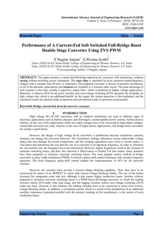
Analysis of on Load Tap Changing Transformer for Substationijtsrd
On load tap changing transformers play important roles in any modern power system since they allow voltages to be maintained at desired levels despite load changes. Traditionally, on load tap changer is a complex mechanical device, which has some deficiencies. On load tap changer of a transformer is presented, which can eliminate excessive conduction losses and suppress the arcing in the diverter switch, which is inherent in traditional on load transformer tap changers. The OLTC provides uninterrupted voltage is regulation of transformers under load. The transformer is equipped with a tapped winding whose tappings are connected with the tap selector of the OLTC. Most of the current commercially available automatic voltage regulators, just measure the low voltage side of the power transformer in order to control OLTC position. In this to improve tap changer control in order to perform properly also during a stressed situation in the 230 33 kV regulating power transformer for the substation. Zin Wah Aung | Aung Thike "Analysis of on Load Tap Changing Transformer for Substation" Published in International Journal of Trend in Scientific Research and Development (ijtsrd), ISSN: 2456-6470, Volume-3 | Issue-5 , August 2019, URL: https://www.ijtsrd.com/papers/ijtsrd26556.pdfPaper URL: https://www.ijtsrd.com/engineering/electrical-engineering/26556/analysis-of-on-load-tap-changing-transformer-for-substation/zin-wah-aung
Speed Control Of Separately Excited Dc Motor Using A High Efficiency Flyback ...IJERA Editor
This paper deals with Speed control of separately excited DC motor using flyback converter with a new non complementary active clamp control method to achieve soft switching and high efficiency for heavy motor load and light load conditions. This is quite attractive for low power application with universal ac inputs, such as external adaptors. With the proposed control technique, the energy in the leakage inductance can be fully recycled. The soft switching can be achieved for the main switch and the absorbed leakage energy is transferred to the output and input side. In the Proposed model the resistive and DC motor is connected to flyback converter and it is simulated with different nominal voltages and rated speed is controlled at different levels for the N-type active clamp flyback converter and P-type active clamp flyback converter respectively. N-type active clamp flyback converter is suitable for high speed variation applications and P-type active clamp flyback converter is suitable for low speed variation applications.
Open Loop and Closed Loop Performance of Switched Reluctance Motor with Vario...IAES-IJPEDS
Switched reluctance motor (SRM) is becoming popular because of its simple construction, robustness and low-maintenance. This motor is very useful for high speed applications because no windings are placed on rotor and can also be used for variable speed applications in industries. Converter is one of the important elements in SRM which plays a very crucial role. In this paper various converter topologies for 6/4 switched reluctance motor and Asymmetric bridge converter topology for 8/6 switched reluctance motor are discussed. Finally a closed loop for each converter topology is proposed. The converter topologies are simulated by using MATLAB/SIMULINK. Constant speed is achieved in closed loop control.
Comparators are basic building elements for designing modern analog and mixed signal systems. Speed and resolution are two important factors which are required for high speed applications. This paper presents a design for an on chip high-speed dynamic latched comparator for high frequency signal digitization. The dynamic latched comparator consists of two cross coupled inverters comprising a total of 9 MOS transistors. The measured and simulation results show that the dynamic latched comparator design has higher speed, low power dissipation and occupying less active area compared to double tail latched and preamplifier based clocked comparators. A new fully dynamic latched comparator which shows lower offset voltage and higher load drivability than the conventional dynamic latched comparators has been designed. With two additional inverters inserted between the input-stage and output-stage of the conventional double-tail dynamic comparator, the gain preceding the regenerative latch stage was improved and the complementary version of the output-latch stage, which has bigger output drive current capability at the same area, was implemented.
This paper presents a phase shifted series resonant converter with step up high frequency transformer to achieve the functions of high output voltage, high power density and wide range of Zero Voltage Switching (ZVS). In this approach, the output voltage is controlled by varying the switching frequency. The controller has been designed to achieve a good stability under different load conditions. The converter will react to the load variation by varying its switching frequency to satisfy the output voltage requirements. Therefore in order to maintain constant output voltage, for light load (50% of the load), the switching frequency will be decreased to meet the desired output, while for the full load (100%) conditions, the switching frequency will be increased. Since the controlled switching frequency is limited by the range between the higher and lower resonant frequencies , the switches can be turned on under ZVS. In this study, a laboratory experiment has been conducted to verify the effectiveness of the system performance.
Test done on Power transformers.
Insulation Resistance test, Winding Resistance test, Ratio Measurements, Magnetic balance test, Tan delta test, DIssolved gas analysis for transformer, Sweep frequency response analysis.
To overcome the problem of mismatched voltage levels between parallel-connected low voltage photovoltaic (PV)
arrays and the higher grid voltage, a hybrid boost three level dc-dc converter is developed based on three level inverter with
the traditional single phase diode clamping. Only one inductor, two capacitors in series, and those power switches and diodes,
which are easy to be integrated, are used for establish the topology with transformerless high voltage gain. The operation
principle of the topology is analyzed, and then the pulse width modulation (PWM) control method is obtained according to
the switching functions about the output pulse voltages of both half-bridges. Therefore, the converter can not only operate
with high voltage gain, but also make the duty cycles of power switches closer to 0.5. A feedforward closed loop control
operation is proposed such that even in varying input the converter is capable of giving a constant output. Finally an
experimental is set up in the laboratory for open loop control operation. All experimental results verify the feasibility of the
circuit and validity of the PWM control method.
Review of Step down Converter with Efficient ZVS OperationIJRST Journal
This paper presents the review of step down converter with efficient ZVS operation. The designed buck converter uses ZCS technique and the function is realized so that the power form is converted from 12V DC 5V DC (1A). A detailed analysis of zero current switching buck converters is performed and a mathematical analysis of the mode of operation is also presented. In order to reduce the switching losses in associated with conventional converters; resonant inductor and resonant capacitor (LC resonant circuit) is applied which helps to turn on-off the switch at zero current. The dc-dc buck converter receives the energy from the input source, when the switch is turned-on. The buck–buck converters have characteristics that warrant a more detailed study. The buck converters under discontinuous conduction mode /continuous conduction mode boundary.
International Journal of Engineering Research and DevelopmentIJERD Editor
Electrical, Electronics and Computer Engineering,
Information Engineering and Technology,
Mechanical, Industrial and Manufacturing Engineering,
Automation and Mechatronics Engineering,
Material and Chemical Engineering,
Civil and Architecture Engineering,
Biotechnology and Bio Engineering,
Environmental Engineering,
Petroleum and Mining Engineering,
Marine and Agriculture engineering,
Aerospace Engineering.
International Journal of Engineering Research and Applications (IJERA) is an open access online peer reviewed international journal that publishes research and review articles in the fields of Computer Science, Neural Networks, Electrical Engineering, Software Engineering, Information Technology, Mechanical Engineering, Chemical Engineering, Plastic Engineering, Food Technology, Textile Engineering, Nano Technology & science, Power Electronics, Electronics & Communication Engineering, Computational mathematics, Image processing, Civil Engineering, Structural Engineering, Environmental Engineering, VLSI Testing & Low Power VLSI Design etc.
SIMULATION ANALYSIS OF CLOSED LOOP DUAL INDUCTOR CURRENT-FED PUSH-PULL CONVER...Journal For Research
The current electronic devices require DC power source, which is taken from a battery or DC power supply. DC-DC converter is utilized to get regulated dc voltage from unregulated one. Switched mode power supply (SMPS) are commonly used in industrial applications, because of more advantages compared to linear power supply. In SMPS we have isolated and non-isolated converters, where isolated converters are frequently used, in order to get more voltage with multiple outputs. So among different isolated converters, push-pull converter is chosen for micro converter applications to obtain high voltage conversion ratio by using HF transformer, due to their better utilization of transformer. New methodology of control is implemented for making ZVS and ZCS at same time and to reduce the number of switches in the secondary side of dual inductor CFPP converter, which is a voltage doubler circuit. This becomes the solution for problem identification. Thus this converter with soft-switching reduces the switching losses.The current-fed push-pull converters are used in many applications like photo-voltaic (PV) power converters for boosting the output voltage. Push-pull converter is chosen for micro converter applications, to obtain high voltage conversion ratio by using high frequency (HF) transformer, due to their better utilization of transformer. This deals with the design of dual inductor CFPP converter, where zero voltage switching (ZVS) and zero current switching (ZCS) is achieved for the primary side of the converter by using secondary switches. Primary side switches are controlled by closed loop control topology. The secondary side is made with voltage doubler to obtain high voltage. Open loop and closed loop control of dual inductor current fed push pull converter simulation is finished by MATLAB/SIMULINK and their outcomes are analyzed.
International Journal of Engineering Research and Applications (IJERA) is a team of researchers not publication services or private publications running the journals for monetary benefits, we are association of scientists and academia who focus only on supporting authors who want to publish their work. The articles published in our journal can be accessed online, all the articles will be archived for real time access.
Our journal system primarily aims to bring out the research talent and the works done by sciaentists, academia, engineers, practitioners, scholars, post graduate students of engineering and science. This journal aims to cover the scientific research in a broader sense and not publishing a niche area of research facilitating researchers from various verticals to publish their papers. It is also aimed to provide a platform for the researchers to publish in a shorter of time, enabling them to continue further All articles published are freely available to scientific researchers in the Government agencies,educators and the general public. We are taking serious efforts to promote our journal across the globe in various ways, we are sure that our journal will act as a scientific platform for all researchers to publish their works online.
Design & Implementation of Zero Voltage Switching Buck ConverterIJERA Editor
Zero voltage switching (ZVS) buck converter is more preferable over hard switched buck converter for low power, high frequency DC-DC conversion applications. In Zero voltage switching converter, turn on & turn off of a switch occurs at zero voltage that results in lower switching losses. In this converter soft switching is achieved by using resonant components. The optimal values of resonant components are determined by using electric functions derived from circuit configuration. This type of soft switched resonant converter offers very low electromagnetic interference (EMI).This study presents the circuit configuration with least components to realize highly efficient zero voltage switching resonant converter. It’s feasibility is confirmed with the developed proto type model and experimental results are verified.
Design of Half Bridge LLC Resonant Converter for Low Voltage Dc ApplicationsIOSRJEEE
An advanced hybrid LLC series resonant converter with united flying-capacitor cell is proposed in this paper to permit the high step-down conversion in the high input voltage applications. The in-built flyingcapacitor branch in the primary side can efficiently share out the primary switch voltage stress related with the half-bridge LLC converters. And the input voltage can be shared correspondingly and automatically between the two series half-bridge components lacking additional balance circuit or control strategies owing to the built-in flying- capacitor cell. Likewise, the inherent soft switching performance in extensive load range that exists in the LLC converters is still kept to decrease the switching losses, which ensures the high efficiency. In addition, the proposed converter can be comprehensive to reduce the switch voltage stress byemploying stacked connection. Finally, a 500∼640 Vinput 48 Voutput 1 kW prototype is built and tested to verify the efficiency of the proposed converter. The results prove that the proposed converter is an excellent candidate for the high input voltage and high step-down dc/dc conversion systems.
International Journal of Engineering Research and Applications (IJERA) is an open access online peer reviewed international journal that publishes research and review articles in the fields of Computer Science, Neural Networks, Electrical Engineering, Software Engineering, Information Technology, Mechanical Engineering, Chemical Engineering, Plastic Engineering, Food Technology, Textile Engineering, Nano Technology & science, Power Electronics, Electronics & Communication Engineering, Computational mathematics, Image processing, Civil Engineering, Structural Engineering, Environmental Engineering, VLSI Testing & Low Power VLSI Design etc.
Wind Energy Conversion System Using PMSG with T-Source Three Phase Matrix Con...IJTET Journal
This paper presents an analysis of a PMSG wind power system using T-Sourcethree phase matrix converter. PMSG using T-Source three phase matrix converterhas advantages that it can provide any desired AC output voltage regardless of DC input with regulation in shoot-through time. In this control system T-Source capacitor voltage can be kept stable with variations in the shoot-through time, maximum power from the wind turbine to be delivered. Inaddition, of a new future, the converter employs a safe-commutation strategy toconduct along a continuous current flow, which results in theelimination of voltage spikes on switches without the need for a snubber circuit. With the use of matrix converter the surely need forrectifier circuit and passive components to store energy arereduced. The MATLAB/Simulinkmodel of the overall system is carried out and theoretical wind energy conversion output load voltage calculations are madeand feasibility of the new topology has been verified and that theconverter can produce an output voltage and output current. This proposed method has greater efficiency and lower cost.
Universal demand for power increases due to continuous development to fulfil all these demand. Resources
are used with optimization. A high efficiency and high power factor converters are the major parts of energy
transfer system. This paper present a general review on single stage forward and flyback converter topologies to get
better its performance. This is paper presents a kind general idea of increasing efficiency and power factor of single
stage forward and fly back converter.
Research Inventy : International Journal of Engineering and Scienceresearchinventy
Research Inventy : International Journal of Engineering and Science is published by the group of young academic and industrial researchers with 12 Issues per year. It is an online as well as print version open access journal that provides rapid publication (monthly) of articles in all areas of the subject such as: civil, mechanical, chemical, electronic and computer engineering as well as production and information technology. The Journal welcomes the submission of manuscripts that meet the general criteria of significance and scientific excellence. Papers will be published by rapid process within 20 days after acceptance and peer review process takes only 7 days. All articles published in Research Inventy will be peer-reviewed.
A ZVS Interleaved Boost AC/DC Converter Using Super Capacitor Power for Hybri...IJMER
International Journal of Modern Engineering Research (IJMER) is Peer reviewed, online Journal. It serves as an international archival forum of scholarly research related to engineering and science education.
SOLID STATE TRANSFORMER - USING FLYBACK CONVERTERAbhin Mohan
FUTURISTIC ELECTRICAL ENGINEERING PROJECT.
A Device that can step up as well as step down coltage and get output as both DC or AC. Total flexibility of Power using DC link by Flyback Coverter.
Welcome to WIPAC Monthly the magazine brought to you by the LinkedIn Group Water Industry Process Automation & Control.
In this month's edition, along with this month's industry news to celebrate the 13 years since the group was created we have articles including
A case study of the used of Advanced Process Control at the Wastewater Treatment works at Lleida in Spain
A look back on an article on smart wastewater networks in order to see how the industry has measured up in the interim around the adoption of Digital Transformation in the Water Industry.
Explore the innovative world of trenchless pipe repair with our comprehensive guide, "The Benefits and Techniques of Trenchless Pipe Repair." This document delves into the modern methods of repairing underground pipes without the need for extensive excavation, highlighting the numerous advantages and the latest techniques used in the industry.
Learn about the cost savings, reduced environmental impact, and minimal disruption associated with trenchless technology. Discover detailed explanations of popular techniques such as pipe bursting, cured-in-place pipe (CIPP) lining, and directional drilling. Understand how these methods can be applied to various types of infrastructure, from residential plumbing to large-scale municipal systems.
Ideal for homeowners, contractors, engineers, and anyone interested in modern plumbing solutions, this guide provides valuable insights into why trenchless pipe repair is becoming the preferred choice for pipe rehabilitation. Stay informed about the latest advancements and best practices in the field.
Student information management system project report ii.pdfKamal Acharya
Our project explains about the student management. This project mainly explains the various actions related to student details. This project shows some ease in adding, editing and deleting the student details. It also provides a less time consuming process for viewing, adding, editing and deleting the marks of the students.
Saudi Arabia stands as a titan in the global energy landscape, renowned for its abundant oil and gas resources. It's the largest exporter of petroleum and holds some of the world's most significant reserves. Let's delve into the top 10 oil and gas projects shaping Saudi Arabia's energy future in 2024.
Hierarchical Digital Twin of a Naval Power SystemKerry Sado
A hierarchical digital twin of a Naval DC power system has been developed and experimentally verified. Similar to other state-of-the-art digital twins, this technology creates a digital replica of the physical system executed in real-time or faster, which can modify hardware controls. However, its advantage stems from distributing computational efforts by utilizing a hierarchical structure composed of lower-level digital twin blocks and a higher-level system digital twin. Each digital twin block is associated with a physical subsystem of the hardware and communicates with a singular system digital twin, which creates a system-level response. By extracting information from each level of the hierarchy, power system controls of the hardware were reconfigured autonomously. This hierarchical digital twin development offers several advantages over other digital twins, particularly in the field of naval power systems. The hierarchical structure allows for greater computational efficiency and scalability while the ability to autonomously reconfigure hardware controls offers increased flexibility and responsiveness. The hierarchical decomposition and models utilized were well aligned with the physical twin, as indicated by the maximum deviations between the developed digital twin hierarchy and the hardware.
Final project report on grocery store management system..pdfKamal Acharya
In today’s fast-changing business environment, it’s extremely important to be able to respond to client needs in the most effective and timely manner. If your customers wish to see your business online and have instant access to your products or services.
Online Grocery Store is an e-commerce website, which retails various grocery products. This project allows viewing various products available enables registered users to purchase desired products instantly using Paytm, UPI payment processor (Instant Pay) and also can place order by using Cash on Delivery (Pay Later) option. This project provides an easy access to Administrators and Managers to view orders placed using Pay Later and Instant Pay options.
In order to develop an e-commerce website, a number of Technologies must be studied and understood. These include multi-tiered architecture, server and client-side scripting techniques, implementation technologies, programming language (such as PHP, HTML, CSS, JavaScript) and MySQL relational databases. This is a project with the objective to develop a basic website where a consumer is provided with a shopping cart website and also to know about the technologies used to develop such a website.
This document will discuss each of the underlying technologies to create and implement an e- commerce website.
About
Indigenized remote control interface card suitable for MAFI system CCR equipment. Compatible for IDM8000 CCR. Backplane mounted serial and TCP/Ethernet communication module for CCR remote access. IDM 8000 CCR remote control on serial and TCP protocol.
• Remote control: Parallel or serial interface.
• Compatible with MAFI CCR system.
• Compatible with IDM8000 CCR.
• Compatible with Backplane mount serial communication.
• Compatible with commercial and Defence aviation CCR system.
• Remote control system for accessing CCR and allied system over serial or TCP.
• Indigenized local Support/presence in India.
• Easy in configuration using DIP switches.
Technical Specifications
Indigenized remote control interface card suitable for MAFI system CCR equipment. Compatible for IDM8000 CCR. Backplane mounted serial and TCP/Ethernet communication module for CCR remote access. IDM 8000 CCR remote control on serial and TCP protocol.
Key Features
Indigenized remote control interface card suitable for MAFI system CCR equipment. Compatible for IDM8000 CCR. Backplane mounted serial and TCP/Ethernet communication module for CCR remote access. IDM 8000 CCR remote control on serial and TCP protocol.
• Remote control: Parallel or serial interface
• Compatible with MAFI CCR system
• Copatiable with IDM8000 CCR
• Compatible with Backplane mount serial communication.
• Compatible with commercial and Defence aviation CCR system.
• Remote control system for accessing CCR and allied system over serial or TCP.
• Indigenized local Support/presence in India.
Application
• Remote control: Parallel or serial interface.
• Compatible with MAFI CCR system.
• Compatible with IDM8000 CCR.
• Compatible with Backplane mount serial communication.
• Compatible with commercial and Defence aviation CCR system.
• Remote control system for accessing CCR and allied system over serial or TCP.
• Indigenized local Support/presence in India.
• Easy in configuration using DIP switches.
1. International Advance Journal of Engineering Research (IAJER)
Volume 3, Issue 2 (February- 2020), PP 01-08
ISSN: 2360-819X
www.iajer.com
Engineering Journal www.iajer.com Page | 1
Research Paper Open Access
Performance of A Current-Fed Soft Switched Full-Bridge Boost
Double Stage Converter Using ZVS PWM
S Nagma Anjum1
G.Pavana Jyothi2
1
Dept. of EEE Dr.KV Subba Reddy College of Engineering for Women, Kurnool, A.P, India
1
Dept. of EEE Dr.KV Subba Reddy College of Engineering for Women, Kurnool, A.P, India
*Corresponding Author: S Nagma Anjum
ABSTRACT: This paper presents a current-fed full-bridge boost dc/ac/dc converter with transformer isolation
operating without switching power dissipation. The output voltage is regulated by dc/ac converter control frequency
changes with a constant turn-off time of transistors. The proposed converter is devoid of parasitic oscillations,
as all of the parasitic capacitances and inductances are included in a resonant tank circuit. The main advantage of
such systems is that they include a capacitive output filter, which is preferred in higher voltage applications.
Moreover, it achieves ZCS for all active switches and zero-voltage switching (ZVS) operation for all diodes on
high voltage side, which is an additional benefit. In this paper, the system operation is first explained, and the
simulation results for optimal mode of operation and sub-optimal mode of operation are presented.
Keyword: Bridge, current-fed, dc/ac/dc converter, resonant.
I. INTRODUCTION
High voltage DC-AC-DC converters with an isolation transformer are used in different types of
electronic applications such as battery chargers and dischargers, uninterruptible power systems, hybrid electric
vehicles. In the case of the applications where low input voltages have to be converted to high output voltages,
current-fed converters are used, whereas in the case of higher power applications, full bridge boost converters
are usually a good choice.
However, the design of high voltage dc-dc converters is problematic because transformer parasitic
elements can change the converter behavior. The transformer leakage inductance causes undesirable voltage
spikes that may damage the circuit components, and the winding capacitance may result in current spikes. A
vital factor that determines the size and the cost of a converter is its operation frequency. In order to minimize
the size and the cost, the frequency has to be maximized. However, higher frequencies result in the increase of
transistor switching losses, and thus, the converter’s effectiveness is limited. For that reason, many solutions
have been proposed to minimize converter switching losses. The most popular control method of bridge
converters is pulse width modulation (PWM). It utilizes a phase-shift control technique with constant frequency
operation. The fixed frequency phase-shift control enables the implementation of ZCS for all converter
switches.
However, the switches must provide a reverse-voltage blocking capability. Thus, they have to be
constructed by means of an MOSFET in series with reverse-voltage blocking diodes. The use of the diodes
increases the component count and cost, although it also causes higher conduction losses. Another solution
proposed to minimize converter switching losses is a PWM boost full-bridge converter, in which the leading
switches realize ZCS under wide load range, and the lagging switches realize zero-voltage switching (ZVS)
under any load. Likewise in this solution, the leading switches have to be connected in series with reverse-
voltage blocking diodes. In addition, a circulating current, which is a result of the introduction of an additional
auxiliary inductance (connected parallel with the primary winding of the transformer), is the source of extra
conduction losses.
2. Performance of A Current-Fed Soft Switched Full-Bridge Boost Double Stage Converter Using…
Engineering Journal www.iajer.com Page | 2
II. DOUBLE STAGE DC/AC/DC CONVERTER
Fig.1: Block Diagram of Double Stage Dc/Ac/Dc Converter
In fig.1 DC supply is given to an Inverter. The Inverter converts the DC power into AC power. The DC
input voltage is converted to AC in order to increase the efficiency of the converter. The boosting operation is
done in the Inverter circuit, which is also a boost converter. Each Mosfet acts as a switch without any switching
losses and facilitates the operation of the converter. Now the boosted voltage is further passed through an
isolation transformer to isolate output from the input variations if any and also the input from the load
variations. The isolation transformer is connected to the rectifier circuit on the other half, where the AC voltage
is converted to the DC output voltage.
III. PROPOSED SYSTEM ARCHITECTURE AND DESCRIPTION:
The proposed converter system is devoid of parasitic oscillations as all the parasitic capacitances and
inductances are included in the resonant tank circuit. The characteristic feature of resonant converters is that the
transformer parasites do not disturb the circuit, because they are used as resonant circuit elements. In a current
fed full bridge boost converter type the overlapping conduction time of the four converter switches is kept
constant and the output voltage is regulated by varying the switching frequency. The conduction time is
particularly calculated to ensure ZCS operation under a wide load range. MOSFET’s and body diodes are used
as the converter switches without the need for any additional diodes in series. The converter transistor turn-off
time is constant and is equal to the time of the parallel connected capacitor overcharge. During the ZCS switch
off-time, the L-C tank circuit resonates. This traverses the voltage across the switch from zero to its peak, and
backdown again to zero. At this point the switch can be reactivated, and lossless zero voltage switching is
facilitated. Therefore the switch transition losses go to zero regardless of operating frequency and input voltage.
This could result in significant savings in power and improvement in efficiency. This feature of the converter
makes it suitable for high frequency and high voltage converter design.
Fig.2. Proposed converter circuit a) Main circuit
3. Performance of A Current-Fed Soft Switched Full-Bridge Boost Double Stage Converter Using…
Engineering Journal www.iajer.com Page | 3
b) Control pulse waveform
The proposed converter scheme is shown in Fig. 2(a). The inductance Ll represents the transformer
leakage inductance, the capacitance C includes the transformer parasitic capacitance, and the capacitances CT
include the transistor parasitic capacitances. The transistor control pulse waveforms are shown in Fig. 2(b). The
converter is controlled by varying the switching frequency f = 1/T, while simultaneously keeping a constant
break between the pulses. Thus, the transistor pulse overlap tov gradually decreases while the switching
frequency increases. The maximal output voltage (power) is achieved in the minimal switching frequency,
which is marked as nominal, i.e., fn.For this frequency, the converter operates in the optimal operation point
while its transistors are switched at zero-voltage and zero-current conditions. This optimal operation point is
achieved by assuming the constant break between the control pulses depending on the resonant circuit elements
and the load resistance nominal (minimal) value. In the optimal operation point, converter currents alternatively
flow through transistors or its external capacitors CT . The transistor body diodes do not participate in current
conduction. During one control period, the following subintervals can be determined: during the pulse overlap
time tov, all the transistors are on, and because of the system symmetry, each of them conducts a half value of
the input current, i.e., Iin/2, and a half value of the output current, i.e., iL/2. During the constant break between
the control pulses, two transistors and two capacitors alternatively conduct T1T4CT3CT2 or T2T3CT1CT4.
Because of the system symmetry, each transistor and each capacitor conducts, as in the previous subinterval,
half values of the input and output currents. Thus, for the system mathematical analysis, there is no need to
divide the entire switching cycle into particular subintervals .When the switching frequency increases above its
nominal value or the load resistance increases above its nominal value, the converter goes to a suboptimal
operation range. In the suboptimal operation state, the constant break between the control pulses is too long for
the capacitors CT to overcharge. Thus, after the capacitor overcharge, an adequate transistor body diode takes
over current conduction. After the body diode current falls to zero, it starts to increase in the transistor at zero
voltage conditions. Based on the overlapping of pulses we can divide into two modes namely optimal and sub-
optimal.
IV. OPTIMAL MODE OF OPERATION
Optimal mode of operation is a mode in which the converter will have lesser switching losses because
of the application of phase shifted pulse width modulation strategy. The proposed soft switched full bridge boost
DC/AC/DC converter is simulated in optimal operation mode analyzed at 250 kHz frequency
4.2. Design Specifications of Soft Switched Converter at Fn=250khz
• Fn = 250KHz, Fr=50hz
• Lin=1e-3H
• CT=7e-9F
• L=16e-6H
• C=29.73e-9F
• Ll=1.4e-6H
• Co=1e-5F
• R load=100W
4.3. Simulation Circuit for Current-Fed Soft Switched Full-Bridge Boost Dc/Ac/Dc Converter at Fn=250
Khz
4. Performance of A Current-Fed Soft Switched Full-Bridge Boost Double Stage Converter Using…
Engineering Journal www.iajer.com Page | 4
powergui
Continuous
io1
i
+ -
io
i
+ -
Vo1
v+
-
Vo
V3
v+
-
V2
v+
-
V1
v+
-
V
v
+
-
Scope1
Ro5
Ro2
Ro
Pulse
Generator 1
Pulse
Generator
M4
G
D
S
M3
G
D
S
M2
G
D
S
M1
G
D
S
Linear Transformer
1 2 L1L
Io1
Display7
3.482
Display 6
3.873
Display5
0.3093
Display 4
0.3987
Display 3
0.5191
Display2
240.6
Display 1
2.314
Display
231.4
DC Voltage Source
D4
D3
D2
D1
Current Measurement
i+
-
Co
7th Harmonic
signal
magnitude
angle
5th Harmonic
signal
magnitude
angle
3rd Harmonic
signal
magnitude
angle
1
Fig.3.Pulses For MOSFETS
5. Performance of A Current-Fed Soft Switched Full-Bridge Boost Double Stage Converter Using…
Engineering Journal www.iajer.com Page | 5
Fig.4.Input Voltage
Fig.5.Output Voltage and Output Current
4.4. Performance Parameters Observed Of Current-Fed Full-Bridge Boost Dc/Ac/Dc Converter
At Fn=250 Khz
• Input voltage Vin=100V
• Output voltage Vout=231.4V
• Output current=2.314 amps
• Pout=531.45W
• Efficiency=94.95%
• Switching loss=28.47W
• Voltage gain=2.314V
Input voltage is given as 100v. We get output voltage as 231.4v. Output voltage is increased by 131v compared
to hard switching converter. So we can use this project where we need high power applications.
V. SUB-OPTIMAL OPERATION MODE
The switches are triggered with conventional triggering pulsed without overlap .Zero voltage switching will be
achieved but the switch is triggered at of very instant of zero voltage crossing of switch voltage (capacitor)
because there is no overlap provided. Soft switched converter is analyzed at 360 kHz frequency.
6. Performance of A Current-Fed Soft Switched Full-Bridge Boost Double Stage Converter Using…
Engineering Journal www.iajer.com Page | 6
5.1. Design Specifications of Soft Switched Converter at Fn=360khz
• Lin=1e-3H
• CT=7e-9F
• L=16e-6H
• C=14.33e-9F
• Ll=1.4e-6H
• Co=1e-5F
• R load=100W
• Fn=360khz
• Fr=50hz
5.2. Simulation Circuit Of Current-Fed Soft Switched Full-Bridge Boost Dc/Ac/Dc Converter At
Fn=360 Khz
powergui
Continuous
io1
i
+ -
io
i
+ -
Vo1
v+
-
Vo
V3
v+
-
V2
v+
-
V1
v+
-
V
v
+
-
Scope 1
Ro5
Ro2
Ro
Pulse
Generator 1
Pulse
Generator
M4
G
D
S
M3
G
D
S
M2
G
D
S
M1
G
D
S
Linear Transformer
1 2 L1L
Io1
Display 7
4.27
Display 6
-7.307 e-016
Display 5
0.0008945
Display 4
0.001175
Display 3
0.001434
Display 2
229 .8
Display 1
2.109
Display
210 .9
DC Voltage Source
D4
D3
D2
D1
Current Measurement
i+
-
Co
7th Harmonic
signal
magnitude
angle
5th Harmonic
signal
magnitude
angle
3rd Harmonic
signal
magnitude
angle
1
Fig.6.Pulses for MOSFETS
7. Performance of A Current-Fed Soft Switched Full-Bridge Boost Double Stage Converter Using…
Engineering Journal www.iajer.com Page | 7
Fig.7.Voltage Across Switch- Condition Of Zero Voltage Switching
Fig.8.Input Voltage
Fig.9.Output Voltage And Output Current
5.3. Performance Parameters Observed Of Current-Fed Full-Bridge Boost Dc/Ac/Dc Converter
at Fn=360 Khz
• Input voltage Vin=100V
• Output voltage Vout=210.9V
• Output current=2.109 amps
8. Performance of A Current-Fed Soft Switched Full-Bridge Boost Double Stage Converter Using…
Engineering Journal www.iajer.com Page | 8
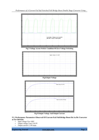
• Pout=85.2W
• Efficiency=94.44%
• Switching loss=29.17W
• Voltage gain=2.109V
VI. CONCLUSION
In this paper current-fed full-bridge dc-ac-dc converter system with transformer isolation has been
proposed.. Detailed Matlab simulation results have been presented to evaluate the performance of the converter.
The simulated and experimental values have shown. The dc/ac converter is controlled by varying the control
frequency and the constant transistor turn-off time. During the whole control range, the transistor current and
voltage waveforms do not overlap, so the switching power dissipations do not occur. The ac/dc rectifier diodes
operate in discontinuous range so their switching power dissipations are also minimized. So a dc-ac-dc
converter can be used for high power application which gives constant dc output voltage with fewer losses. The
main features of the proposed converter are as follows
1) The primary benefit of using a Full-Bridge dc-dc converter is its power handling capabilities and stability.
2) The ac-dc rectifier diodes operate in discontinuous range with zero voltage switching so their switching
power dissipations are also minimized.
REFERENCES
[1]. R. Y. Chen, R. L. Lin, T. I. Liang, I. F. Chen, and K.C.Tseng,“Current fed full-bridge boost converter
with zero current switching for high voltage applications,” in Conf. Rec. IAS Annu. Meeting, 2005,
vol. 3, pp. 2000–2006.
[2]. C. Iannello, S. Luo, and I. Batarseh, “Full bridge ZCS PWM converter for high-voltage high-power
applications,” IEEE Trans. Aerosp. Electron.Syst.,[[ vol. 38, no. 2, pp. 515–526, Apr. 2002.
[3]. L. Zhou and X. Ruan, “A zero-current and zero-voltage-switching PWM boost full-bridge converter,”
in Proc. IEEE PESC Conf., 2003, vol. 2, pp. 957–962.
[4]. R. Watson and F. C. Lee, “A soft-switched, full-bridge boost converter employing an active-clamp
circuit,” in Proc. IEEE PESC Conf., 1996, pp. 1948–1954.
[5]. K. Wang, L. Zhu, H. Odendaal, J. Lai, and F. C. Lee, “Design, implementation, and experimental
results of bi-directional full-bridge DC/DC converter with unified soft-switching scheme and soft-
starting capability”
[6]. Belaguli and A. K. S. Bhat, “Operation of the LCC-type parallel resonant converter as a low harmonic
rectifier,” IEEE Trans. Ind. Electron., vol. 46, no. 2, pp. 288–299, Apr. 1999
[7]. Garcia, V., et al. “An optimized dc-to-dc converter topology for high-voltage pulse-load applications”.
(1994
[8]. Weinberg, A. H., and Schreuders, J. “A high-power high- voltage dc-dc converter for space
applications”.IEEE Transactions on Power Electronics (1986)
[9]. Hino, H., et al “Resonant PWM inverter linked dc-dc converter using parasitic impedance of high-
voltage transformer and its applications to X-ray generator”. . (1988)
[10]. Kim, Y. J., et al. “Comparative performance evaluations of high-voltage transformer parasitic
parameter resonant inverter-linked high-power dc-dc converter with phase-shifted PWM scheme. .
(1995).
[11]. J.A.sabate, V.Vlatkovuc, R.B.Ridely, FC.Lee and B.L.Cho “design consideration for high voltage high
power full bridge zero voltage switching PWM converters” in proc. Applied power electroics conf. and
exposition (APEC ’90) ( 1990)
[12]. W.Chen, F.C.Lee, M.M.Jovanovic, J.ASabate, “ A comparative study of class of full bridge zero-
voltage-switched PWM converters,” in proc. IEEE Applied Power Electronics Conf., (1995)