Download to read offline
![© 2022, IRJET | Impact Factor value: 7.529 | ISO 9001:2008 Certified Journal | Page 735
A Self-Balancing Switched Capacitor Multilevel Inverter Structure with
Six-fold Gain Factor
P. Ajay Kumar1, K.S. Ravi Kumar2
1MTech Scholar, Department of Electrical and Electronics Engineering, MVGR College of Engineering,
Vizianagaram, Andhra Pradesh, India
2Associate Professor, Department of Electrical and Electronics Engineering, MVGR College of Engineering,
Vizianagaram, Andhra Pradesh, India
---------------------------------------------------------------------***---------------------------------------------------------------------
Abstract - In this article, a novel self-balancing switched
capacitor multilevel inverter structure with six-fold gain
factor is proposed. This inverter's design callsfora singleDC
supply, 3 capacitors, and 14 switches to generate an output
voltage with 13 levels. The power storage mechanism used
by this inverter construction allows it to automatically
balance itself by charging and discharging capacitors in
series and parallel with a DC source. The proposed inverter
does not require a back-end H-bridge, therefore each switch
is not subjected to as much voltage stress as under a peak
load. The result is a striking reduction in Total Blocking
Voltage (TBV) from 88Vdc to 33Vdc and Maximum Blocking
Voltage (MBV) from 6Vdc to 4Vdc for similar topologies and
thus makes it a preferable choice for renewable energy
applications. The proposed SBSCI topology modes of
operation, capacitor design and control strategy are
delineated. A thorough comparison with existing literature
demonstrates the proposed topology's affordability and
compactness. The performanceandviabilityofthesuggested
topology are validated using the MATLAB/SIMULINK
software.
Key Words: Maximum Blocking Voltage (MBV), Self-
Balancing Mechanism, Total Cost Function (TCF),
Voltage gain, Self-BalancingSwitched CapacitorInverter
(SBSCI).
1.INTRODUCTION
Due to their better waveform nature and reduced switching
voltage stress of each power switch, multilevel dc-ac power
converters are currently the most widely used solution in
industries for high-power applications withmediumvoltage
levels. Itsignificantlybenefitsapplicationsrequiringmedium
voltage and high power, such as those for electric vehicles
and renewable energy sources. [1],[2]. MLIs have gained
popularity because to their intrinsic advantages, which
include lowering switching frequency, lowering switching
stress, and improving voltage and current waveforms by
decreasing harmonics [3]. Researchers from all around the
world are paying close attention to the neutral point
clamped (NPC), flying capacitor (FC), and cascadedH-bridge
(CHB) inverters, which have already achieved commercial
viability [4]. Although the MLIs being advantageous it also
suffers with some flaws like capacitors balancing issues and
requirement of complex circuits in case of flying capacitor
inverter (FC) and Neutral point clamped inverter(NPC).The
cascaded H-bridge inverter(CHB)necessitatesnumerousDC
supply’s, increasing the system's size and cost. All of these
conventional MLIs have one thing in common: they aren't
capable of raising voltage. To address this issue for the
researchers, switching capacitors are the best option. The
switching capacitor topology-based MLI has become more
prevalent in recent years [5].
Up until thispoint,differentswitchedcapacitortopologies
have mainly been used in single-phase systems, with the
most popular variety being created by stacking switched
capacitor topologies with an inverting H-bridge. The ac
output voltage is produced by the H-bridge on the end side,
while the circuit on the front side produces a range of dc
levels. A traditional series/parallel switchingcapacitordc/dc
multilevel circuit, as well as its streamlined variant and an
updated structure, are employed to power the H-bridge [9].
When an H-bridge is used, the switches are under more
voltage stress. By using a different commonly utilized
integrated circuit created by sandwiching a switching
capacitor based multilevel converter circuit between two
half bridges, it is possible to get beyond the restrictions of
these topologies [6-8]. In [10], a modular switchedcapacitor
topology was analyzed while keeping all of the benefits of
switched capacitortopologies.Although[9-10]usessingledc
source to attain 13-levels at the output but it provides with
high switching stress across the switches that limits the
topology to work for low power applications. Some
topologies suffer with the least gain. However, some
topologies that aim to increase highvoltagelevelsareunable
to reduce switching stress [10]. Some switched capacitor
topologies requires auxiliary H-bridge for polarity
generation [11]. The single source topology requires
complex algorithms and voltage balancing auxiliary circuits
in order to attain high power density. This causes the
system's size and cost to grow. The literature analysis
mentioned above provides room todevelopa novel topology
that possesses the following appealing qualities. An SBSCI
topology with 13 levels and a six-foldgainfactorisdescribed
in this article.
International Research Journal of Engineering and Technology (IRJET) e-ISSN: 2395-0056
Volume: 9 Issue: 10 | Oct 2022 www.irjet.net p-ISSN: 2395-0072](https://image.slidesharecdn.com/irjet-v9i10116-221110080034-9b9ab2ca/75/A-Self-Balancing-Switched-Capacitor-Multilevel-Inverter-Structure-with-Six-fold-Gain-Factor-1-2048.jpg)


![International Research Journal of Engineering and Technology (IRJET) e-ISSN: 2395-0056
Volume: 9 Issue: 10 | Oct 2022 www.irjet.net p-ISSN: 2395-0072
© 2022, IRJET | Impact Factor value: 7.529 | ISO 9001:2008 Certified Journal | Page 740
TAB2 Comparative Assessment of 13SBSCI topology with current literatures
Reference Gain(G) TSV MBV Cost
Function
[6] 16 0 4 16 2 3 34 13 6 10.76
[7] 14 0 2 11 2 2 32 13 6 9.07
[8] 11 0 1 10 2 2 38 13 6 9.23
[9] 19 0 5 19 1 6 39 13 6 6.30
[10] 29 0 5 29 1 6 88 13 6 11.61
[11] 14 2 4 14 2 6 34 13 6 10.46
Proposed 14 0 3 14 1 6 33 13 4 4.92
(TSV) can be calculated as the summation of maximum
voltage stress across the each individual switches. The cost
function (CF) of an inverter is described as:
equation 6
The weight factor, which is equal to the importance of
switching components, is denoted by the symbol ( . TAB2
compares switchedcapacitortopologieswithvariousvoltage
gains at the same voltage levels. The design cost of the
inverters is increased by the topology [10]’s extensiveuse of
semiconductor components, which also raises the overall
standing voltage. On the other hand, there are fewer
switches in the topologies [7] [8] that are put under more
strain than the source voltage. To offset the output voltage
rise by a factor of six, the total cost function (TCF) is high.
This is an important factor to take into account because the
Maximum blocking voltage of the switchissixtimeslargerin
[6-11] designs. The required voltage level, according to
[9][10], can only be reached employing several capacitorsin
its construction. The design described in [11] uses several
diodes, which raises count of semiconductors usage and
raises losses, which is another important concern. In some
topologies [6-11] the maximum blocking voltage (MBV) is
high which limits to low power applications.Fig5depictsthe
comparison assessment of 13SBSCI topology with current
literature in terms of component count in Fig5(a), Total cost
function (TCF) and TBV in Fig5(b), and gain &MBV in
Fig5(c).
5. RESULTS AND DISCUSSION
Using the values listed in TAB3, MATLAB/Simulink tools
have been utilized to simulate the proposed 13SBSCIdesign.
In dynamic conditions, the proposed switching capacitor
topology was tested. Inductive-resistive load configuration
output waveform is shown in Fig. 6.
Fig5 Comparative Assessment of 13SBSCI topology with current literatures](https://image.slidesharecdn.com/irjet-v9i10116-221110080034-9b9ab2ca/75/A-Self-Balancing-Switched-Capacitor-Multilevel-Inverter-Structure-with-Six-fold-Gain-Factor-6-2048.jpg)

![International Research Journal of Engineering and Technology (IRJET) e-ISSN: 2395-0056
Volume: 9 Issue: 10 | Oct 2022 www.irjet.net p-ISSN: 2395-0072
© 2022, IRJET | Impact Factor value: 7.529 | ISO 9001:2008 Certified Journal | Page 742
2500 Hz for 5 cycles and 5000 Hz for next 5 cycles with
output voltage, current and trio capacitors output voltage.
Fig9 Proposed topology workability under step change in
load
Fig10 Frequency change form 2500 Hz to 5000 Hz of
proposed 13SBSCI topology
From Fig11 it depicts thattheswitchingstressvoltageacross
each switched used in designed 13SBSCI topology. The
maximum blocking voltage in proposed SBSCI structure is
just four times the sourcevoltage.Theproposedarchitecture
can therefore be used in high power applications. The
aforementioned scenarios demonstrate the suggested
switched capacitor topology's superior responsiveness.
Fig11 Switching stress of proposed 13SBSCI topology
6. CONCLUSION
The topology discussed in this study is a low switch-count,
boost-capable, self-voltage-balanced 13-level SBSCI
topology. The suggested architecture uses only 14 switches
to generate thirteen levels and boosts the output to 6 times
from one DC supply. When compared to other switched
capacitor topologies that have been previously published,
the proposed topology displays a lower TSV and MBV. A
detailed investigation of performance comparisons showed
that the proposed switched capacitor topology outperforms
comparable prior-art. The enhanced voltage boosting
capabilities also makes the topology suitable for renewable
energy applications. The results of the simulationconfirmed
the circuit's functionality and showed voltage boosting
capability for wide range of M.Is, good voltage and current
regulation for load and frequency variation, and reduced
switching stress. The proposed switched capacitor topology
offers strong structural and functional benefits for high
voltage applications.
REFERENCES
[1] P. R. Bana, K. P. Panda, R. T. Naayagi, P. Siano, and G.
Panda, ‘‘Recentlydeveloped reduced switch multilevel
inverter for renewable energy integration and drives
application: Topologies, comprehensive analysis and
comparative evaluation,’’ IEEE Access, vol. 7,pp.54888–
54909, 2019.
[2] B. P. Reddy, M. A. Rao, M. Sahoo, and S. Keerthipati, ‘‘A
fault-tolerant multilevel inverter for improving the
performance of a pole–phase modulated nine-phase
induction motor drive,’’ IEEE Trans. Ind. Electron.,vol.
65, no. 2, pp. 1107–1116, Feb. 2018.
[3] J. S. M. Ali and V. Krishnaswamy, ‘‘An assessment of
recent multi- level inverter topologies with reduced
power electronics components for renewable](https://image.slidesharecdn.com/irjet-v9i10116-221110080034-9b9ab2ca/75/A-Self-Balancing-Switched-Capacitor-Multilevel-Inverter-Structure-with-Six-fold-Gain-Factor-8-2048.jpg)
![International Research Journal of Engineering and Technology (IRJET) e-ISSN: 2395-0056
Volume: 9 Issue: 10 | Oct 2022 www.irjet.net p-ISSN: 2395-0072
© 2022, IRJET | Impact Factor value: 7.529 | ISO 9001:2008 Certified Journal | Page 743
applications,’’ Renew. Sustain. Energy Rev., vol. 82, no.
3,pp. 3379–3399, Feb. 2018.
[4] M. Vijeh, M. Rezanejad, E. Samadaei,andK.Bertilsson,“A
general review of multilevel inverters based on main
sub-modules: Structural point of view,” in IEEE
Transactions on Power Electronics, vol. 34, no. 10, pp.
9479–9502, Oct. 2019.
[5] Jena, Kasinath, Chinmoy Kumar Panigrahi, and Krishna
Kumar Gupta. "A 6X-Voltage-Gain 13-Level Inverter
With Self-Balanced Switched-Capacitors." CPSS
Transactions on PowerElectronicsandApplications 7,no.
1, pp.94-102, 2022.
[6] T. Roy, P. K. Sadhu, and A. Dasgupta, “Cross-Switched
Multilevel Inverter Using Novel Switched Capacitor
Converters,” IEEE Trans. Ind. Electron.,vol.66,no.11,pp.
8521–8532, Nov. 2019.
[7] E. Samadaei, M. Kaviani, and K. Bertilsson, “A 13-levels
Module ( K-Type ) with two DC sources for Multilevel
Inverters,” IEEE Trans. Ind. Electron., vol. 66, no. 7,
pp.5186-5196, 2018.
[8] M. D. Siddique, S. Mekhilef, A. Sarwar, A. Alam, and N. M.
Shah, “Dual asymmetrical dc voltage source based
switched capacitor boost multilevel inverter topology,”
IET Power Electron., vol. 13, no. 7, pp. 1481–1486, 2020.
[9] Y. Hinago and H. Koizumi, “A switched-capacitor
inverter using series/parallel conversionwithinductive
load,” IEEE Trans. Ind. Electron., vol. 59, no. 2, pp. 878–
887, Feb. 2012.
[10] A. Taghvaie, J. Adabi, and M. Rezanejad, “ASelf-Balanced
Step-Up Multilevel Inverter Based on Switched-
Capacitor Structure,” IEEE Trans. Power Electron., vol.
33, no. 1, pp. 199–209, Jan 2018.
[11] T. Roy and P. K. Sadhu, “A Step-Up Multilevel Inverter
Topology Using Novel Switched Capacitor Converters
with Reduced Components,” IEEE Trans. Ind. Electron.,
vol. 68, no. 1, pp. 236–247, Jan. 2021.
“P. Ajay Kumar has received
his Bachelor of Technology
degree in Electrical &
Electronics Engineeringfrom
MVGR CollegeofEngineering,
India in 2020. He is currently
pursuing final year in Master
of Technology in the
specialization of Power
Systems, MVGR College of
Engineering, Andhra
Pradesh, India.”
“K S RAVI KUMAR (M’20)
was born in Kharagpur India
on April 18, 1977. He did his
B. Tech degree in Electrical
engineering in SVHCE,
Nagarajuna University,
Machilipatnam, A.P, India, in
1999, did his M.Tech degree
in control systems from NIT
Kurukshetra in 2002.
Presently he is pursuing his
PhD in Electrical
Engineering, at KL
University, Guntur,A.P.,India
since 2015. He is also
working in MVGR College of
engineering, Vizianagaram,
A.P., India since 2002,
presently as Associate
Professor. His Research
Interests are in the area of
Bidirectional DC-DC
Converters in Power
Electronics, ElectricVehicles,
Embedded Controllers and
Artificial Intelligence.
Mr.Kalamchety was a
member of IET since 2017.
He is also a member of IEEE.
He has around 8
International Journalsand19
International Conference
Publications and 3 Indian
patents published to his
credit. ”
BIOGRAPHIES](https://image.slidesharecdn.com/irjet-v9i10116-221110080034-9b9ab2ca/75/A-Self-Balancing-Switched-Capacitor-Multilevel-Inverter-Structure-with-Six-fold-Gain-Factor-9-2048.jpg)

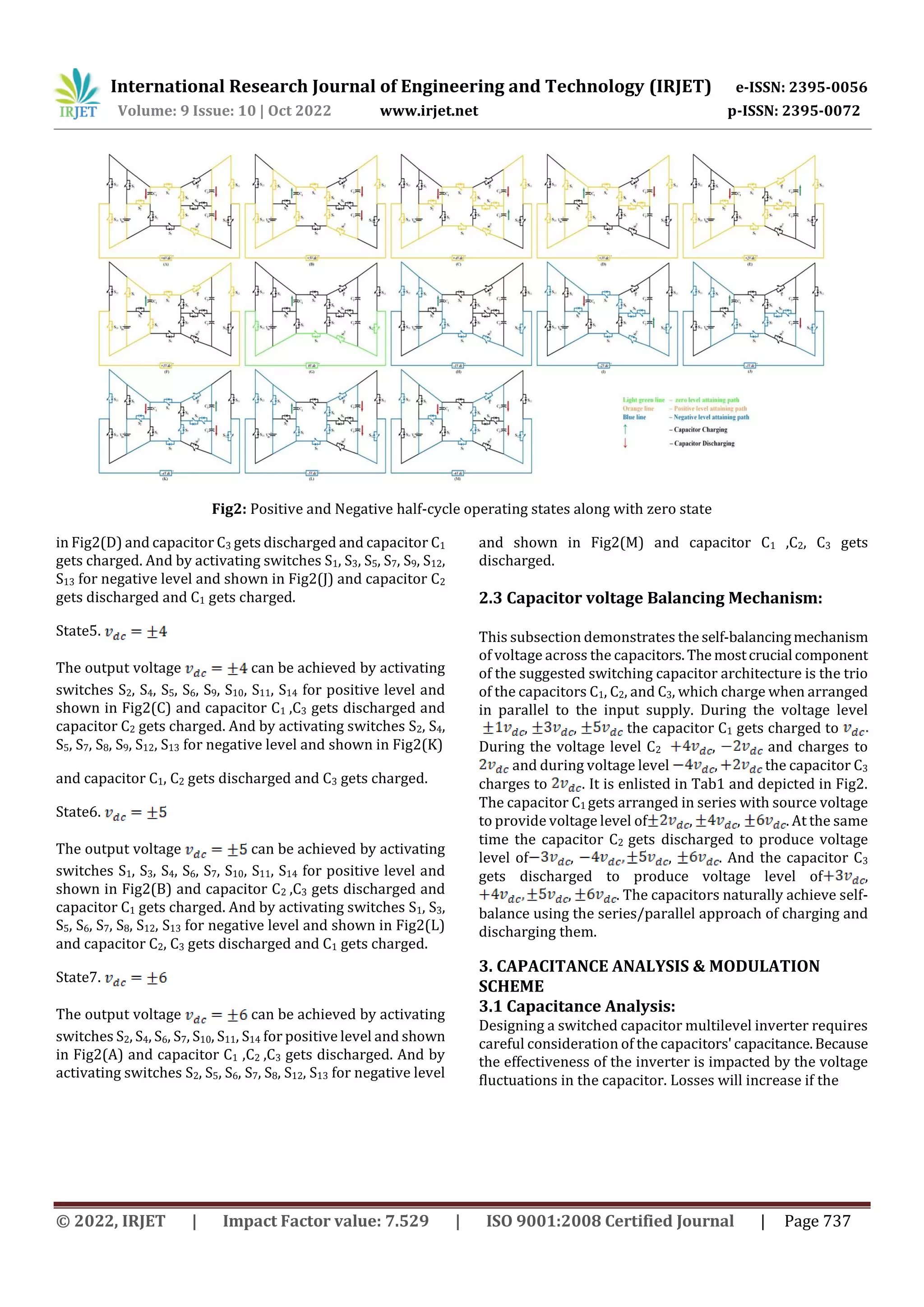
This document describes a novel self-balancing switched capacitor multilevel inverter structure that can generate 13 voltage levels from a single DC supply using 3 capacitors and 14 switches. Key features include its ability to automatically balance capacitor voltages through series and parallel charging and discharging, and its reduction in maximum blocking voltage stress across switches compared to similar topologies. The document outlines the circuit configuration, operating principle with 13 states, capacitor sizing analysis, and modulation scheme. Simulation results validate the performance and viability of the proposed topology, which is well-suited for renewable energy applications due to its reduced switching stresses.


