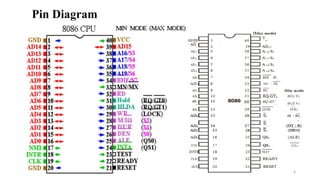
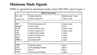
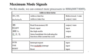
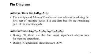
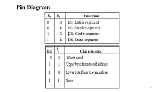
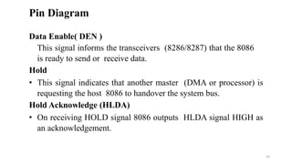
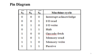
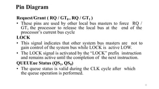
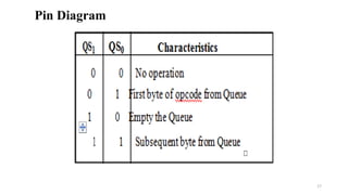
Lecture 11: 8086 Pin Diagram
Microprocessor and Assembly
Language
8086 Microprocessor
2
Pin Diagram
3
Minimum Mode Signals
4
•8086 is operated in minimum mode when MN/MX’ pin to logic 1.
Minimum Mode Signals
5
Maximum Mode Signals
6
•In this mode, we can connect more processors to 8086(8087/8089).
Maximum Mode Signals
7
Address / Data Bus (AD15–AD0)
• The multiplexed Address/ Data bus acts as address bus during the
first part of machine cycle (T1) and data bus for the remaining
part of the machine cycle.
Address/Status (A19/S6,A18/S5,A17/S4,A16/S3)
• During T1 these are the four most significant address lines
for memory operations.
• During I/O operations these lines are LOW.
Pin Diagram
8
Pin Diagram
9
Read(RD)
• This signal is used to read data from memory or I/O device
which reside on the 8086 local bus.
Ready
• If this signal is low the 8086 enters into WAITstate.
• The READY signal from memory/ IO is synchronized by the
8284A clock generator to form READY.
• This signal is active HIGH.
Interrupt Request (INTR)
• It is a level triggered maskable interrupt request.
• A subroutine is vectored via an interrupt vector lookup table
located in system memory.
Pin Diagram
10
TEST
• This input is examined by the “Wait” instruction.
• If the TEST input is LOW execution continues,
• otherwise the processor waits in an ``Idle’’ state.
Non-Maskable Interrupt (NMI)
• It is an edge triggered input which causes a type 2 interrupt.
• NMI is not maskable internally by software.
Reset
• This signal is used to reset the 8086.
• It causes the processor to immediately terminate its present
activity.
• The signal must be active HIGH for at least four clock cycles.
• It restarts execution when RESET returns LOW.
Pin Diagram
11
Clock (CLK)
• This signal provides the basic timing for the processor
and bus controller.
• The clock frequency may be 5 MHz or 8 MHz or 10 MHz
depending on the version of 8086.
VCC
• It is a +5V power supply pin.
Ground (GND)
• Two pins (1 and 20) are connected to ground ie, 0 V power
supply.
Minimum/Maximum (MN/ MX )
• This pin indicates what mode the processor is to operate in.
Pin Diagram
12
MEMORY / IO (M/ IO)
• It is used to distinguish a memory access from an I/O access. M =
HIGH, I/O = LOW.
WRITE(WR)
• It indicates that the processor is performing a write memory or
write I/O cycle, depending on the state of the M/ IO signal.
• Interrupt Acknowledge (INTA) This signal indicates
recognition of an interrupt request. It is used as a read strobe for
interrupt acknowledge cycles.
Address Latch Enable (ALE)
• This signal is used to demultiplex the AD0-AD15 into A0-A15 and
D0-D15. It is a HIGH pulse active during T1 of any bus cycle.
Pin Diagram
13
Data Enable( DEN )
This signal informs the transceivers (8286/8287) that the 8086
is ready to send or receive data.
Hold
• This signal indicates that another master (DMA or processor) is
requesting the host 8086 to handover the system bus.
Hold Acknowledge (HLDA)
• On receiving HOLD signal 8086 outputs HLDA signal HIGH as
an acknowledgement.
Pin Diagram
14
Pin Diagram
15
Request/Grant ( RQ / GT0 , RQ / GT1 )
• These pins are used by other local bus masters to force RQ /
GT1 the processor to release the local bus at the end of the
processor’s current bus cycle
LOCK
• This signal indicates that other system bus masters are not to
gain control of the system bus while LOCK is active LOW.
• The LOCK signal is activated by the “LOCK” prefix instruction
and remains active until the completion of the next instruction.
QUEUEue Status (QS1, QS0)
• The queue status is valid during the CLK cycle after which
the queue operation is performed.
Pin Diagram
16
Pin Diagram
17
18

Lecture 11 8086 Pin Diagram.pptx

  • 1.
    Lecture 11: 8086Pin Diagram Microprocessor and Assembly Language
  • 2.
  • 3.
  • 4.
    Minimum Mode Signals 4 •8086is operated in minimum mode when MN/MX’ pin to logic 1.
  • 5.
  • 6.
    Maximum Mode Signals 6 •Inthis mode, we can connect more processors to 8086(8087/8089).
  • 7.
  • 8.
    Address / DataBus (AD15–AD0) • The multiplexed Address/ Data bus acts as address bus during the first part of machine cycle (T1) and data bus for the remaining part of the machine cycle. Address/Status (A19/S6,A18/S5,A17/S4,A16/S3) • During T1 these are the four most significant address lines for memory operations. • During I/O operations these lines are LOW. Pin Diagram 8
  • 9.
  • 10.
    Read(RD) • This signalis used to read data from memory or I/O device which reside on the 8086 local bus. Ready • If this signal is low the 8086 enters into WAITstate. • The READY signal from memory/ IO is synchronized by the 8284A clock generator to form READY. • This signal is active HIGH. Interrupt Request (INTR) • It is a level triggered maskable interrupt request. • A subroutine is vectored via an interrupt vector lookup table located in system memory. Pin Diagram 10
  • 11.
    TEST • This inputis examined by the “Wait” instruction. • If the TEST input is LOW execution continues, • otherwise the processor waits in an ``Idle’’ state. Non-Maskable Interrupt (NMI) • It is an edge triggered input which causes a type 2 interrupt. • NMI is not maskable internally by software. Reset • This signal is used to reset the 8086. • It causes the processor to immediately terminate its present activity. • The signal must be active HIGH for at least four clock cycles. • It restarts execution when RESET returns LOW. Pin Diagram 11
  • 12.
    Clock (CLK) • Thissignal provides the basic timing for the processor and bus controller. • The clock frequency may be 5 MHz or 8 MHz or 10 MHz depending on the version of 8086. VCC • It is a +5V power supply pin. Ground (GND) • Two pins (1 and 20) are connected to ground ie, 0 V power supply. Minimum/Maximum (MN/ MX ) • This pin indicates what mode the processor is to operate in. Pin Diagram 12
  • 13.
    MEMORY / IO(M/ IO) • It is used to distinguish a memory access from an I/O access. M = HIGH, I/O = LOW. WRITE(WR) • It indicates that the processor is performing a write memory or write I/O cycle, depending on the state of the M/ IO signal. • Interrupt Acknowledge (INTA) This signal indicates recognition of an interrupt request. It is used as a read strobe for interrupt acknowledge cycles. Address Latch Enable (ALE) • This signal is used to demultiplex the AD0-AD15 into A0-A15 and D0-D15. It is a HIGH pulse active during T1 of any bus cycle. Pin Diagram 13
  • 14.
    Data Enable( DEN) This signal informs the transceivers (8286/8287) that the 8086 is ready to send or receive data. Hold • This signal indicates that another master (DMA or processor) is requesting the host 8086 to handover the system bus. Hold Acknowledge (HLDA) • On receiving HOLD signal 8086 outputs HLDA signal HIGH as an acknowledgement. Pin Diagram 14
  • 15.
  • 16.
    Request/Grant ( RQ/ GT0 , RQ / GT1 ) • These pins are used by other local bus masters to force RQ / GT1 the processor to release the local bus at the end of the processor’s current bus cycle LOCK • This signal indicates that other system bus masters are not to gain control of the system bus while LOCK is active LOW. • The LOCK signal is activated by the “LOCK” prefix instruction and remains active until the completion of the next instruction. QUEUEue Status (QS1, QS0) • The queue status is valid during the CLK cycle after which the queue operation is performed. Pin Diagram 16
  • 17.
  • 18.