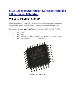
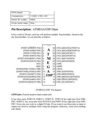
https://technoelectronics44.blogspot.com/202
0/08/atmega-328p.html
What is ATMEGA-328P
The ATmega328 is a single-chip microcontroller created by Atmel with inside
the megaAVR family, later Microchip Technology acquired Atmel in 2016.
The alternative to the ATMEGA328 is “Pico power” MCU (ATMEGA328P)
 ATMEGAp-328
 ATMEGA-328p
 ATMEGA-328PB, ATMEGA-328PB(AUTOMOTIVE)-advance to the
ATMEGA-328P(more UART, SPI, Memory...)
ATMEGA-328P-TQFP
ATMEGA-328P-PU DIP
USER MANUAL: User manual
Technical specifications
ATMEGA-328P
Processor 8-Bit AVR-RISC
External Oscillator 16Mhz
Architecture Harvard
Flash memory type Enabled
Flash memory 32kb
EEPROM 1Kb
SRAM 2kb
ADC 10-bit (6 channels)
Performance 1 MIPS per 1 MHZ
Write/erase cycles flash =10,000
EEPROM=100,000
Timers 2-8bit, 1-16bit Timers
Pins 28(DIP),32(TQFP)
Operating voltage 2.7v to 5.5v
Operating
temperature
-40 ͦC to +125 ͦC.
PWM channels 6
Communication 1-UART, 2-SPI, 1-I2C
Internal RC oscillator 8MHZ
I/O pin current ratings 40ma
Pin Description: ATMEGA328P-28pin
It has a total of 28 pins, each pin will perform multiple functionalities, based on the
pin functionalities we can describe as follows.
ATMEGA-328P Pin diagram
GPIO pins: General purpose input-output pins
It has three ports PORT-B, PORT-C, PORT-D. PORT-B has eight pins from PB0-
PB7, PORT-C has seven pins from PC0-PC6 and PORT-D has eight pins from PD0-
PD7. Every pin can work as a digital I/O pin. If you want to use these pins as input or
output you need to configure them using the program, otherwise, some error readings
will obtain.
PORT-B =PB0, PB1, PB2,PB3, PB4,PB5,PB6,PB7.
PORT-C =PC0, PC1, PC2,PC3, PC4,PC5,PC6.
PORT-D =PD0,PD1, PD2,PD3,PD4,PD5,
PD6,PD7.
Communication pins: Serial communication
Serial communication supported by ATMEGA328P: 1-UART, 1-I2C, 2-SPI
UART: Universal asynchronous receiver transmitter
It has one UART communication it has two pins RX, TX
 RX (Receive data) –PD0/2
 TX (Transmit data)-PD1/3
I2C: Inter-Integrated Circuit.
 SCL (Serial Clock) –PC5/28
 SDA (Serial Data)-PC4/27
SPI: serial peripheral interface
 SCK (Clock) –PB5/19
 MISO (Master In Slave Out) –PB4/18
 MOSI (Master Out Slave IN) –PB3/17
 SS (Slave Select) –PB2/16
INTERRUPTS: External interrupts
 Interrupts are use full to execute the high priority task.
 It has two external interrupts
 INT0-External Interrupt Source 0-PD2/4
 INT1- External Interrupt Source 1-PD3/5
ADC: Analog to Digital Converter (10-BIT)
It has six ADC channels
ADC0-PC0/23
ADC1-PC1/24
ADC2-PC2/25
ADC3-PC3/26
ADC4-PC4/27
ADC5-PC5/28
TIMERS: Timer/Counter
It has two 16 bit timers
 T0-Timer/counter 0-PD4/6
 T1- Timer/counter 1-PD5/11
Comparator
 AIN0-Analog comparator positive input, configure as an input pin and disable
the pullup resistor-PD6/12
 AIN1-Analog comparator negative input, configure as an input pin and disable
the pullup resistor-PD7/13
CLOCK
To execute the set of instructions we need to provide the clock source
 XTAL1-External clock source pin 0 (Crystal oscillator) used to all chip clock
source except internal RC oscillator—PB6/9
 XTAL2- External clock source pin 1 (Crystal oscillator)- -PB7/10
 CLK0- divides the system clock-PB0/14
 TOSC1 –Timer oscillator pin1, used only when the internal clock frequency as
chip clock source-PB6/9
 TOSC2 –Timer oscillator pin2, used only when the internal clock frequency as
chip clock source-PB7/10
PCINT: Pin change Interrupt (PCINT0-PCINT23)
Its interesting feature is any of the pins we can configure as an interrupt pin, So we set the
functionality of the pin as an interrupt.
Capture and PWM channel (OC (Output compare),IC(Input compare))
OC: Output compare match, it provides the external output to the Timer/Counter match output.
IC: Input compare pin, it acts as an input capture pin for the corresponding pin.
 OC0A-PD6/12
 OC0B-PD5/11
 OC1A-PB1/15
 OC1B-PB2/16
 OC2A-PB3/17
 OC2B-PD3/5
 ICP1-PB0/14
RESET: Reset pin-PC6/1
It is an active LOW state pin, it acts as an input pin when it is programmed it depends on power-
on reset and brown-out reset functions. When it is unprogrammed it depends on the
input reset circuitry.
AREF: Analog reference voltage--21
ARef is the external power supply to the ADC module, by default ADC takes the Vcc (5V) of the
controller.
If you want to set any customized voltage to ADC module you have to use the ARef pin.
AVcc: Analog power pin-20
It is used to activate the ADC operation.
POWER: Power supply pins
 VCC – 7
 GND- 8, 22
HOW TO USE ATMEGA328P
If you want to work with any microcontroller you need to remember two things
 Hardware setup
 Software setup
Hardware setup
Microcontroller the developing board needs minimum hardware configuration, those are
power supply the unit, operating frequency (crystal unit), Reset circuitry and finally, you
need to set up a boot loader for the flash program.
Software setup
To develop any application program you have a compiler or IDE. Download the compiler
and install it from core foundry website (MICROCHIP). For ATMEGA328 u have to prefer -
ATMEL-STUDIO IDE
Download link: CLICK HERE
NOTE: For easy purpose go to ARDUINO(ATMEGA 328P) controller.
Applications
 Embedded products design.
 Voltage controller unit
 Digital Energy meters
 Familiar with the Arduino family.
Reference links:
https://www.microchip.com/wwwproducts/en/atmega328p
http://ww1.microchip.com/downloads/en/DeviceDoc/Atmel-7810-Automotive-Microcontrollers-
ATmega328P_Datasheet.pdf
https://en.wikipedia.org/wiki/ATmega328.

ATmega328p

  • 1.
    https://technoelectronics44.blogspot.com/202 0/08/atmega-328p.html What is ATMEGA-328P TheATmega328 is a single-chip microcontroller created by Atmel with inside the megaAVR family, later Microchip Technology acquired Atmel in 2016. The alternative to the ATMEGA328 is “Pico power” MCU (ATMEGA328P)  ATMEGAp-328  ATMEGA-328p  ATMEGA-328PB, ATMEGA-328PB(AUTOMOTIVE)-advance to the ATMEGA-328P(more UART, SPI, Memory...) ATMEGA-328P-TQFP
  • 2.
    ATMEGA-328P-PU DIP USER MANUAL:User manual Technical specifications ATMEGA-328P Processor 8-Bit AVR-RISC External Oscillator 16Mhz Architecture Harvard Flash memory type Enabled Flash memory 32kb EEPROM 1Kb SRAM 2kb ADC 10-bit (6 channels) Performance 1 MIPS per 1 MHZ Write/erase cycles flash =10,000 EEPROM=100,000 Timers 2-8bit, 1-16bit Timers Pins 28(DIP),32(TQFP) Operating voltage 2.7v to 5.5v Operating temperature -40 ͦC to +125 ͦC.
  • 3.
    PWM channels 6 Communication1-UART, 2-SPI, 1-I2C Internal RC oscillator 8MHZ I/O pin current ratings 40ma Pin Description: ATMEGA328P-28pin It has a total of 28 pins, each pin will perform multiple functionalities, based on the pin functionalities we can describe as follows. ATMEGA-328P Pin diagram GPIO pins: General purpose input-output pins It has three ports PORT-B, PORT-C, PORT-D. PORT-B has eight pins from PB0- PB7, PORT-C has seven pins from PC0-PC6 and PORT-D has eight pins from PD0- PD7. Every pin can work as a digital I/O pin. If you want to use these pins as input or output you need to configure them using the program, otherwise, some error readings will obtain.
  • 4.
    PORT-B =PB0, PB1,PB2,PB3, PB4,PB5,PB6,PB7. PORT-C =PC0, PC1, PC2,PC3, PC4,PC5,PC6. PORT-D =PD0,PD1, PD2,PD3,PD4,PD5, PD6,PD7. Communication pins: Serial communication Serial communication supported by ATMEGA328P: 1-UART, 1-I2C, 2-SPI UART: Universal asynchronous receiver transmitter It has one UART communication it has two pins RX, TX  RX (Receive data) –PD0/2  TX (Transmit data)-PD1/3 I2C: Inter-Integrated Circuit.  SCL (Serial Clock) –PC5/28  SDA (Serial Data)-PC4/27
  • 5.
    SPI: serial peripheralinterface  SCK (Clock) –PB5/19  MISO (Master In Slave Out) –PB4/18  MOSI (Master Out Slave IN) –PB3/17  SS (Slave Select) –PB2/16 INTERRUPTS: External interrupts  Interrupts are use full to execute the high priority task.  It has two external interrupts  INT0-External Interrupt Source 0-PD2/4  INT1- External Interrupt Source 1-PD3/5 ADC: Analog to Digital Converter (10-BIT) It has six ADC channels ADC0-PC0/23 ADC1-PC1/24 ADC2-PC2/25 ADC3-PC3/26 ADC4-PC4/27 ADC5-PC5/28 TIMERS: Timer/Counter It has two 16 bit timers  T0-Timer/counter 0-PD4/6  T1- Timer/counter 1-PD5/11 Comparator  AIN0-Analog comparator positive input, configure as an input pin and disable the pullup resistor-PD6/12  AIN1-Analog comparator negative input, configure as an input pin and disable the pullup resistor-PD7/13
  • 6.
    CLOCK To execute theset of instructions we need to provide the clock source  XTAL1-External clock source pin 0 (Crystal oscillator) used to all chip clock source except internal RC oscillator—PB6/9  XTAL2- External clock source pin 1 (Crystal oscillator)- -PB7/10  CLK0- divides the system clock-PB0/14  TOSC1 –Timer oscillator pin1, used only when the internal clock frequency as chip clock source-PB6/9  TOSC2 –Timer oscillator pin2, used only when the internal clock frequency as chip clock source-PB7/10 PCINT: Pin change Interrupt (PCINT0-PCINT23) Its interesting feature is any of the pins we can configure as an interrupt pin, So we set the functionality of the pin as an interrupt. Capture and PWM channel (OC (Output compare),IC(Input compare)) OC: Output compare match, it provides the external output to the Timer/Counter match output. IC: Input compare pin, it acts as an input capture pin for the corresponding pin.  OC0A-PD6/12  OC0B-PD5/11  OC1A-PB1/15  OC1B-PB2/16  OC2A-PB3/17  OC2B-PD3/5  ICP1-PB0/14 RESET: Reset pin-PC6/1 It is an active LOW state pin, it acts as an input pin when it is programmed it depends on power- on reset and brown-out reset functions. When it is unprogrammed it depends on the input reset circuitry. AREF: Analog reference voltage--21 ARef is the external power supply to the ADC module, by default ADC takes the Vcc (5V) of the controller. If you want to set any customized voltage to ADC module you have to use the ARef pin.
  • 7.
    AVcc: Analog powerpin-20 It is used to activate the ADC operation. POWER: Power supply pins  VCC – 7  GND- 8, 22 HOW TO USE ATMEGA328P If you want to work with any microcontroller you need to remember two things  Hardware setup  Software setup Hardware setup Microcontroller the developing board needs minimum hardware configuration, those are power supply the unit, operating frequency (crystal unit), Reset circuitry and finally, you need to set up a boot loader for the flash program. Software setup To develop any application program you have a compiler or IDE. Download the compiler and install it from core foundry website (MICROCHIP). For ATMEGA328 u have to prefer - ATMEL-STUDIO IDE Download link: CLICK HERE NOTE: For easy purpose go to ARDUINO(ATMEGA 328P) controller. Applications  Embedded products design.  Voltage controller unit  Digital Energy meters  Familiar with the Arduino family. Reference links:
  • 8.