

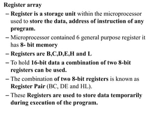


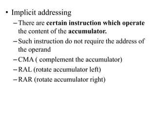


![Stack ,I/O and Machine control
Group
• PUSH rp [push the content of register pair to stack)
• PUSH PSW [push the program status to word]
• POP rp [pop the content of register pair which
was saved from the stack]
• IN PORT
• OUT PORT
• EI (enable interrupts)](https://image.slidesharecdn.com/unit2-230816093951-5415d103/85/MECHATRONICS-UNIT-2-8085-MICROPROCESSOR-AND-8051-MICROCONTROLLER-pptx-44-320.jpg)


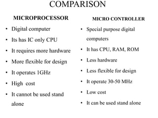

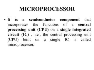
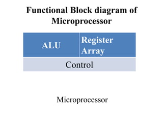
The document provides information on microprocessors and microcontrollers. It discusses the 8085 microprocessor, including its architecture, registers, addressing modes, instruction sets and timing diagrams. It also covers the 8051 microcontroller, describing its features such as RAM, ROM, timers/counters, serial ports, I/O ports and interrupts. A comparison of microprocessors and microcontrollers is given, noting microcontrollers are specialized computers that integrate CPU, memory and I/O components.