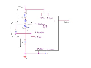
Inv Amp.
Trigger
input
(1/3)Vcc
Vref
Reset3
2
74
6
1
5
+
-
V+V-
OUT
OS1
OS2
U3
3
2
74 6
1
5
+
-
V+V-OUT
OS1
OS2
1
4
13
3
2
12
J
K
CLR
Q
Q
CLK
5k
5k
5k
VCC
6
5
2
7
1
8
4
3
Threshold
Control
Discharge output
(2/3)Vcc
(1/3)Vcc
Q1
Q2
V
• Initially The o/p Q is HIGH
• Therefore o/p of 555(3 pin) is LOW
• The –Ve going input at pin 2(Trigger) is less than Vcc/3, the
output of Lower comparator goes to HIGH and sets the FF i.e.
Q=1
• If The voltage at pin 6(Threshold) is greater than 2Vcc/3
then the upper comparator goes high and resets the FF i.e.
Q=0
• The reset is effective when the i/p is less than 0.4 V.
• The Q2 serves as a buffer to isolate the reset input from The
FF and Q1.
3
2
74
6
1
5
+
-
V+V-
OUT
OS1
OS2
U3
3
2
74 6
1
5
+
-
V+V-OUT
OS1
OS2
1
4
13
3
2
12
J
K
CLR
Q
Q
CLK
5k
5k
5k
V9
R17
C1
6
5
2
7
1
8
4
3
Trigger
I/P
(1/3)Vcc
Reset
Inv. Amp
Output
Vref
• In stand by state FF holds Q1 on, Thus clamping the
external Capacitor to GND, i.e O/p =0.
• The –Ve going input at pin 2(Trigger) is less than Vcc/3,
the output of Lower comparator goes to HIGH and sets the
FF i.e. Q=1. Therefore Q1 is off, o/p is ON(1) and C is
unclamped
• The voltage across C rises exponentially through R
towards Vcc with the time constant of RC (T).
• The Voltage across C increases more than (2/3)Vcc the
upper comparator resets the FF i.e Q1 is on
• The C discharges to GND potential.
Vc=Vcc(1-e-t/RC)
At t=T Vc= (2/3)Vcc
Therefore (2/3)Vcc =Vcc(1-e-T/RC) OR T=RC ln(1/3)
OR T= 1.1 RC Sec therefore the timing interval is
independent of supply voltage.
• Once triggered, the output is remains high until T elapses (RC)
• If a –Ve going reset pulse applied at Pin-4 during the timing
cycle, Q2 and Q1 are On and C is immediately discharged.
• even if the reset is released, o/p remains LOW until a –Ve
going trigger is applied at pin-2.
0
0
0
1
2
34
5
6
7
8
GND
TRIGGER
OUTPUTRESET
CONTROL
THRESHOLD
DISCHARGE
VCC
0.01micro
1k
1n
R
C
Trigger
i/p
Output
Missing Pulse Detector Mono-stable Circuit
0
00
1n
C6
1n
1
2
34
5
6
7
8
GND
TRIGGER
OUTPUTRESET
CONTROL
THRESHOLD
DISCHARGE
VCC
Re
C
Trigger
output
R2
R1
Linear Ramp Generator

t
c idt
c
v
0
1
  EEcEBEBBEcc iRRIRIRIVV
RR
R


 1
21
1
)(
)(
21
211
RRR
RRVVR
i
E
BEcc



t
RRCR
RRVVR
V
E
BEcc
c 



)(
)(
21
211
T
RRCR
RRVVR
V
E
BEcc
cc 



)(
)(
3
2
21
211
)(
)(
3
2
211
21
RRVVR
RRCRV
T
BEcc
Ecc



0
1n
1
2
34
5
6
7
8
GND
TRIGGER
OUTPUTRESET
CONTROL
THRESHOLD
DISCHARGE
VCC
C
Trigger
output
Modulating
i/p
Pulse width Modulator
3
2
74
6
1
5
+
-
V+V-
OUT
OS1
OS2
U3
3
2
74
6
1
5
+
-
V+V-
OUT
OS1
OS2
1
4
13
3
2
12
J
K
CLR
Q
Q
CLK
5k
5k
R17
R17
5k
Ra
Rb
Vcc
C
0.01 Micro F
Vref
Power Amp
1
3
4
5
6
7
7
8
Output
2
Astable Operation
0
100
12
1
555
2 Trigger
6 Threshold
7 Discharge
8 Vcc 4 Reset
1 GND 5 Control
Output
RA
RB
C
+Vcc
0
100
R11
1k
R12
1k
555
2 Trigger
6 Threshold
7 Discharge
8 Vcc 4 Reset
1 GND 5 Control
Output
0.01μF
0.01μF
RA (50k)
RB(47k)
Rc (10k)
5v
FSK Generator
555
2 Trigger
6 Threshold
7 Discharge
8 Vcc 4 Reset
1 GND 5 Control
Output
0
100
RA
RB
Modulating
signal
Pulse Position
Modulator
U5
555alt
1
2
3
4
5
6
7
8
GND
TRIGGER
OUTPUT
RESET
CONTROL
THRESHOLD
DISCHARGE
VCC
Output
Input Vi
Vcc
R1(100k)
R2(100k)
Vcc/2
Schmitt Trigger
555
2 Trigger
6 Threshold
7 Discharge
8 Vcc 4 Reset
1 GND 5 Control
Output

555 timer