SlideShare a Scribd company logo
July 1998
®
N
DIP8
(Plastic Package)
D
SO8
(Plastic Micropackage)
1
2
3
4 5
6
7
8 1 - GND
2 - Trigger
3 - Output
4 - Reset
5 - Control voltage
6 - Threshold
7 - Discharge
8 - VCC
PIN CONNECTIONS (top view)
.LOW TURN OFF TIME
.MAXIMUM OPERATING FREQUENCY
GREATER THAN 500kHz
.TIMING FROM MICROSECONDS TO HOURS
.OPERATES IN BOTH ASTABLE AND
MONOSTABLE MODES
.HIGH OUTPUT CURRENT CAN SOURCE OR
SINK 200mA
.ADJUSTABLE DUTY CYCLE
.TTL COMPATIBLE
.TEMPERATURE STABILITY OF 0.005%
PERo
C
ORDER CODES
Part
Number
Temperature
Range
Package
N D
NE555 0o
C, 70o
C • •
SA555 –40o
C, 105o
C • •
SE555 –55
o
C, 125
o
C • •
DESCRIPTION
The NE555monolithictiming circuitisa highlystable
controllercapableofproducingaccuratetime delays
or oscillation. In the time delay mode of operation,
the time is precisely controlled by one external re-
sistorandcapacitor.Forastableoperationasanos-
cillator, the free running frequency and the duty cy-
cle are both accurately controlled with two external
resistors and one capacitor.The circuit may be trig-
gered and reset on falling waveforms, and the out-
put structure can source or sink up to 200mA. The
NE555 is available in plastic and ceramic minidip
packageand in a 8-lead micropackage and inmetal
can package version.
NE555
SA555 - SE555
GENERAL PURPOSE SINGLE BIPOLAR TIMERS
1/10
THRESHOLD
COMP
5kΩ
5kΩ
5kΩ
TRIGGER
R
FLIP-FLOP
S
Q
DISCHARGE
OUT
INHIBIT/
RESET
RESET
COMP
S - 8086
S
+
CONTROL VOLTAGE
VCC
BLOCK DIAGRAM
OUTPUT
CONTROL
VOLTAGE
THRESHOLD
COMPARATOR
VCC
R1
4.7kΩ
R2
830Ω
Q5 Q6 Q7 Q8 Q9
R3
4.7kΩ
R4
1kΩ
R8
5kΩ
Q1
Q2 Q3
Q4
Q10
Q11 Q12
Q13
THRESHOLD
TRIGGER
RES ET
DISCHARGE
G N D
2
4
7
1
Q14
Q15
R5
10kΩ
R6
100kΩ
R7
100kΩ
R10
5kΩ
Q17
Q16 Q18
R9
5kΩ D2
R16
100Ω
R15
4.7kΩ
R14
220Ω
Q24
Q23
R17
4.7kΩ
3
Q22
Ρ13
D1
Q19
Q20
Q21
R12
6.8kΩ
5
TRIGGER COMPARATOR FLIP FLOP
R11
5kΩ
3.9kΩ
SCHEMATIC DIAGRAM
ABSOLUTE MAXIMUM RATINGS
Symbol Parameter Value Unit
Vcc Supply Voltage 18 V
Toper Operating Free Air Temperature Range for NE555
for SA555
for SE555
0 to 70
–40 to 105
–55 to 125
o
C
Tj Junction Temperature 150
o
C
Tstg Storage Temperature Range –65 to 150
o
C
NE555/SA555/SE555
2/10
ELECTRICAL CHARACTERISTICS
Tamb = +25o
C, VCC = +5V to +15V (unless otherwise specified)
Symbol Parameter
SE555 NE555 - SA555
Unit
Min. Typ. Max. Min. Typ. Max.
ICC Supply Current (RL ∞) (- note 1)
Low State VCC = +5V
VCC = +15V
High State VCC = 5V
3
10
2
5
12
3
10
2
6
15
mA
Timing Error (monostable)
(RA = 2k to 100kΩ, C = 0.1µF)
Initial Accuracy - (note 2)
Drift with Temperature
Drift with Supply Voltage
0.5
30
0.05
2
100
0.2
1
50
0.1
3
0.5
%
ppm/°C
%/V
Timing Error (astable)
(RA, RB = 1kΩ to 100kΩ, C = 0.1µF,
VCC = +15V)
Initial Accuracy - (note 2)
Drift with Temperature
Drift with Supply Voltage
1.5
90
0.15
2.25
150
0.3
%
ppm/°C
%/V
VCL Control Voltage level
VCC = +15V
VCC = +5V
9.6
2.9
10
3.33
10.4
3.8
9
2.6
10
3.33
11
4
V
Vth Threshold Voltage
VCC = +15V
VCC = +5V
9.4
2.7
10
3.33
10.6
4
8.8
2.4
10
3.33
11.2
4.2
V
Ith Threshold Current - (note 3) 0.1 0.25 0.1 0.25 µA
Vtrig Trigger Voltage
VCC = +15V
VCC = +5V
4.8
1.45
5
1.67
5.2
1.9
4.5
1.1
5
1.67
5.6
2.2
V
Itrig Trigger Current (Vtrig = 0V) 0.5 0.9 0.5 2.0 µA
Vreset Reset Voltage - (note 4) 0.4 0.7 1 0.4 0.7 1 V
Ireset Reset Current
Vreset = +0.4V
Vreset = 0V
0.1
0.4
0.4
1
0.1
0.4
0.4
1.5
mA
VOL Low Level Output Voltage
VCC = +15V, IO(sink) = 10mA
IO(sink) = 50mA
IO(sink) = 100mA
IO(sink) = 200mA
VCC = +5V, IO(sink) = 8mA
IO(sink) = 5mA
0.1
0.4
2
2.5
0.1
0.05
0.15
0.5
2.2
0.25
0.2
0.1
0.4
2
2.5
0.3
0.25
0.25
0.75
2.5
0.4
0.35
V
VOH High Level Output Voltage
VCC = +15V, IO(source) = 200mA
IO(source) = 100mA
VCC = +5V, IO(source) = 100mA
13
3
12.5
13.3
3.3
12.75
2.75
12.5
13.3
3.3
V
Notes : 1. Supply current when output is high is typically 1mA less.
2. Tested at VCC = +5V and VCC = +15V.
3. This will determine the maximum value of RA + RB for +15V operation the max total is R = 20MΩ and for 5V operation
the max total R = 3.5MΩ.
OPERATING CONDITIONS
Symbol Parameter SE555 NE555 - SA555 Unit
VCC Supply Voltage 4.5 to 18 4.5 to 18 V
Vth, Vtrig, Vcl, Vreset Maximum Input Voltage VCC VCC V
NE555/SA555/SE555
3/10
ELECTRICAL CHARACTERISTICS (continued)
Symbol Parameter
SE555 NE555 - SA555
Unit
Min. Typ. Max. Min. Typ. Max.
Idis(off) Discharge Pin Leakage Current
(output high) (Vdis = 10V)
20 100 20 100 nA
Vdis(sat) Discharge pin Saturation Voltage
(output low) - (note 5)
VCC = +15V, Idis = 15mA
VCC = +5V, Idis = 4.5mA
180
80
480
200
180
80
480
200
mV
tr
tf
Output Rise Time
Output Fall Time
100
100
200
200
100
100
300
300
ns
toff Turn off Time - (note 6) (Vreset = VCC) 0.5 0.5 µs
Notes : 5. No protection against excessive Pin 7 current is necessary, providing the package dissipation rating will not be exceeded.
6. Time mesaured from a positive going input pulse from 0 to 0.8x VCC into the threshold to the drop from high to low of the
output trigger is tied to treshold.
Figure 1 : Minimum Pulse Width Required for
Trigering
Figure 2 : Supply Current versus SupplyVoltage
Figure 3 : Delay Time versus Temperature Figure 4 : Low Output Voltage versus Output
Sink Current
NE555/SA555/SE555
4/10
Figure 5 : Low Output Voltage versus Output
Sink Current
Figure 6 : Low Output Voltage versus Output
Sink Current
Figure 7 : High Output Voltage Drop versus
Output
Figure 8 : Delay Time versus Supply Voltage
Figure 9 : PropagationDelay versus Voltage
Level of Trigger Value
NE555/SA555/SE555
5/10
CAPACITOR VOLTAGE = 2.0V/div
t = 0.1 ms / div
INPUT = 2.0V/div
OUTPUT VOLTAGE = 5.0V/div
R1 = 9.1kΩ, C1 = 0.01µF, R = 1kΩL
Figure 11
Reset
Trigger
Output
R1
C1
Control Voltage
0.01µF
NE555
= 5 to 15VVCC
4
2
3
1
5
6
7
8
Figure 10
C
(µF)
10
1.0
0.1
0.01
0.001
10 100 1.0 10 100 10 (t )d
µs µs ms ms ms s
10M
Ω
1M
Ω
100kΩ
10kΩ
R
1=
1kΩ
Figure 12
APPLICATION INFORMATION
MONOSTABLE OPERATION
In the monostable mode, the timer functions as a
one-shot.Referring to figure 10 the external capaci-
tor is initially held discharged by a transistorinside
the timer.
The circuit triggers on a negative-goinginput signal
when thelevel reaches1/3 Vcc. Once triggered,the
circuit remains in this state until the set time has
elapsed, even if it is triggered again during this in-
terval.The durationof theoutputHIGHstateisgiven
by t = 1.1 R1C1 and is easily determined by
figure 12.
Notice that since the charge rate and the threshold
levelof the comparatorarebothdirectlyproportional
to supply voltage, the timing intervalis independent
of supply. Applying a negativepulse simultaneously
to the reset terminal (pin 4) and the trigger terminal
(pin 2) during the timing cycle discharges the exter-
nalcapacitorand causesthe cycleto start over.The
timing cycle now starts on the positive edge of the
reset pulse. During the time the reset pulse in ap-
plied, the output is driven to its LOW state.
When a negativetriggerpulse is appliedtopin 2, the
flip-flop is set, releasing the short circuit across the
externalcapacitor anddriving the outputHIGH. The
voltage across the capacitor increases exponen-
tially with the time constantτ =R1C1. When the volt-
ageacross the capacitorequals2/3 Vcc, the compa-
ratorresetsthe flip-flop which thendischargethe ca-
pacitor rapidly and drivers the output to its LOW
state.
Figure 11shows theactual waveforms generatedin
this mode of operation.
When Reset is not used, it should be tied high to
avoid any possibly or false triggering.
ASTABLE OPERATION
When the circuit is connected as shown in figure 13
(pin 2and 6 connected)ittriggersitself andfreeruns
as a multivibrator. The external capacitor charges
through R1 and R2 and discharges through R2 only.
Thus the dutycycle may beprecisely set bythe ratio
of these two resistors.
In the astable mode of operation, C1 charges and
dischargesbetween 1/3 Vcc and 2/3 Vcc. As in the
triggeredmode,thechargeanddischarge timesand
therefore frequency are independentof the supply
voltage.
NE555/SA555/SE555
6/10
t = 0.5 ms / div
OUTPUT VOLTAGE = 5.0V/div
CAPACITOR VOLTAGE = 1.0V/div
R1 = R2 = 4.8kΩ, C1= 0.1µF, R = 1kΩL
Figure 14
C
(µF)
10
1.0
0.1
0.01
0.001
0.1 1 10 100 1k 10k f (Hz)o
1M
Ω
R1
+
R2
=
10M
Ω
100kΩ
10kΩ
1kΩ
Figure 15 : Free Running Frequency versus R1,
R2 and C1
Figure 14showsactualwaveformsgeneratedin this
mode of operation.
The charge time (output HIGH) is given by :
t1 = 0.693 (R1 + R2) C1
and the discharge time (outputLOW) by :
t2 = 0.693 (R2) C1
Thus the total period T is given by :
T = t1 + t2 = 0.693 (R1 + 2R2) C1
The frequency ofoscillation is them :
f =
1
T
=
1.44
(R1 + 2R2) C1
and may be easily found by figure 15.
The duty cycle is given by :
D =
R2
R1 + 2R2
Output 3
4 8
7
5
1
R1
C12
6
R2
Control
Voltage
NE555
VCC = 5 to 15V
0.01µF
Figure 13
PULSE WIDTH MODULATOR
When the timer is connected in the monostable
mode and triggered with a continuous pulse train,
theoutputpulse width can be modulatedby a signal
applied to pin 5. Figure 16 shows the circuit.
Trigger
Output
R
C
NE555
2
4
3
1
5
6
7
Modulation
Input
8
A
VCC
Figure 16 : Pulse Width Modulator.
NE555/SA555/SE555
7/10
LINEAR RAMP
When the pullup resistor, RA, in the monostablecir-
cuitis replacedbya constantcurrentsource,alinear
ramp is generated. Figure 17 shows a circuit con-
figuration that will perform this function.
Trigger
Output
C
NE555
2
4
3
1
5
6
7
8
E
VCC
0.01µF
R2
R1R
2N4250
or equiv.
Figure 17.
Out
RA
C
NE55
2
4
3
1
5
6
7
8
VCC
51kΩ
RB
22kΩ
0.01µF
VCC
0.01µF
Figure 19 : 50%Duty Cycle Oscillator.
Figure 18 shows waveformsgeneratorby the linear
ramp.
The time interval is given by :
T =
(2/3 VCC RE (R1+ R2) C
R1 VCC − VBE (R1+ R2)
VBE = 0.6V
Figure 18 : Linear Ramp.
VCC = 5V Top trace : input 3V/DIV
Time = 20µs/DIV Middle trace : output 5V/DIV
R1 = 47kΩ Bottom trace : output 5V/DIV
R2 = 100kΩ Bottom trace : capacitor voltage
RE = 2.7kΩ 1V/DIV
C = 0.01µF
50% DUTY CYCLE OSCILLATOR
For a 50% duty cycle the resistors RA and RE may
beconnectedasin figure19.Thetime preriodforthe
output high is the same as previous,
t1 = 0.693 RA C.
For the output low it is t2 =
[(RARB) ⁄ (RA + RB)] CLn



RB − 2RA
2RB − RA



Thus the frequencyof oscillation is f =
1
t1 + t2
Note that this circuit will not oscillate if RB is greater
than 1/2 RA because the junction of RA and RB can-
notbring pin2 down to 1/3 VCC andtriggerthelower
comparator.
ADDITIONAL INFORMATION
Adequate power supply bypassing is necessary to
protect associated circuitry. Minimum recom-
mended is 0.1µF in parallel with 1µF electrolytic.
NE555/SA555/SE555
8/10
PM-DIP8.EPS
PACKAGE MECHANICAL DATA
8 PINS - PLASTIC DIP
Dimensions
Millimeters Inches
Min. Typ. Max. Min. Typ. Max.
A 3.32 0.131
a1 0.51 0.020
B 1.15 1.65 0.045 0.065
b 0.356 0.55 0.014 0.022
b1 0.204 0.304 0.008 0.012
D 10.92 0.430
E 7.95 9.75 0.313 0.384
e 2.54 0.100
e3 7.62 0.300
e4 7.62 0.300
F 6.6 0260
i 5.08 0.200
L 3.18 3.81 0.125 0.150
Z 1.52 0.060
DIP8.TBL
NE555/SA555/SE555
9/10
PM-SO8.EPS
PACKAGE MECHANICAL DATA
8 PINS - PLASTIC MICROPACKAGE (SO)
Dimensions
Millimeters Inches
Min. Typ. Max. Min. Typ. Max.
A 1.75 0.069
a1 0.1 0.25 0.004 0.010
a2 1.65 0.065
a3 0.65 0.85 0.026 0.033
b 0.35 0.48 0.014 0.019
b1 0.19 0.25 0.007 0.010
C 0.25 0.5 0.010 0.020
c1 45
o
(typ.)
D 4.8 5.0 0.189 0.197
E 5.8 6.2 0.228 0.244
e 1.27 0.050
e3 3.81 0.150
F 3.8 4.0 0.150 0.157
L 0.4 1.27 0.016 0.050
M 0.6 0.024
S 8
o
(max.)
SO8.TBL
Information furnished is believed to be accurate and reliable. However, STMicroelectronics assumes no responsibility for the
consequences of use of such information nor for any infringement of patents or other rights of third parties which may result
from its use. No license is granted by implication or otherwise under any patent or patent rights of STMicroelectronics. Specifi-
cations mentioned in this publication are subject to change without notice. This publication supersedes and replaces all infor-
mation previously supplied. STMicroelectronics products are not authorized for use as critical components in life support
devices or systems without express written approval of STMicroelectronics.
© The ST logo is a trademark of STMicroelectronics
© 1998 STMicroelectronics – Printed in Italy – All Rights Reserved
STMicroelectronics GROUP OF COMPANIES
Australia - Brazil - Canada - China - France - Germany - Italy - Japan - Korea - Malaysia - Malta - Mexico - Morocco
The Netherlands - Singapore - Spain - Sweden - Switzerland - Taiwan - Thailand - United Kingdo m- U.S.A.
ORDERCODE:
NE555/SA555/SE555
10/10

More Related Content

What's hot

38 hc43ym
38 hc43ym38 hc43ym
38 hc43ym
Quang Hoàng
 
Analog Electronics TIMER IC 555
Analog Electronics TIMER IC 555Analog Electronics TIMER IC 555
Analog Electronics TIMER IC 555
Prabhat Matang
 
Datasheet lm358
Datasheet lm358Datasheet lm358
Datasheet lm358
Domingo Cordova
 
Ciclotron pwp8000 4 ab
Ciclotron   pwp8000 4 abCiclotron   pwp8000 4 ab
Ciclotron pwp8000 4 ab
Muniz Rodrigues
 
Digital timer
Digital timerDigital timer
Digital timer
PrasadPurohit1988
 
HA17741 General Purpose Operational Amplifier
HA17741 General Purpose Operational AmplifierHA17741 General Purpose Operational Amplifier
HA17741 General Purpose Operational Amplifier
Yong Heui Cho
 
Lm358
Lm358Lm358
Ciclotron tip3000 2h ii
Ciclotron   tip3000 2h iiCiclotron   tip3000 2h ii
Ciclotron tip3000 2h ii
Muniz Rodrigues
 
Catalogo 2010
Catalogo 2010Catalogo 2010
Catalogo 2010
Lenin Illich
 
Original Digital Transistor KRC105 C105M C105 100mA 50V TO-92 New
Original Digital Transistor KRC105 C105M C105 100mA 50V TO-92 NewOriginal Digital Transistor KRC105 C105M C105 100mA 50V TO-92 New
Original Digital Transistor KRC105 C105M C105 100mA 50V TO-92 New
AUTHELECTRONIC
 
Data Sheet IC KIA6040
Data Sheet IC KIA6040Data Sheet IC KIA6040
Data Sheet IC KIA6040
arwicaksono
 
Transformer vector group_test_conditions
Transformer vector group_test_conditionsTransformer vector group_test_conditions
Transformer vector group_test_conditions
SARAVANAN A
 
Ciclotron tip3000 2 ab ii
Ciclotron   tip3000 2 ab iiCiclotron   tip3000 2 ab ii
Ciclotron tip3000 2 ab ii
Muniz Rodrigues
 
System Block Diagram 2-9-16
System Block Diagram 2-9-16System Block Diagram 2-9-16
System Block Diagram 2-9-16
Brendan Moon
 
Ciclotron pwp12000 2 h
Ciclotron   pwp12000 2 hCiclotron   pwp12000 2 h
Ciclotron pwp12000 2 h
Muniz Rodrigues
 
Ciclotron pwp20000 2 h
Ciclotron   pwp20000 2 hCiclotron   pwp20000 2 h
Ciclotron pwp20000 2 h
Muniz Rodrigues
 
Ciclotron pwp16000 2 h
Ciclotron   pwp16000 2 hCiclotron   pwp16000 2 h
Ciclotron pwp16000 2 h
Muniz Rodrigues
 

What's hot (17)

38 hc43ym
38 hc43ym38 hc43ym
38 hc43ym
 
Analog Electronics TIMER IC 555
Analog Electronics TIMER IC 555Analog Electronics TIMER IC 555
Analog Electronics TIMER IC 555
 
Datasheet lm358
Datasheet lm358Datasheet lm358
Datasheet lm358
 
Ciclotron pwp8000 4 ab
Ciclotron   pwp8000 4 abCiclotron   pwp8000 4 ab
Ciclotron pwp8000 4 ab
 
Digital timer
Digital timerDigital timer
Digital timer
 
HA17741 General Purpose Operational Amplifier
HA17741 General Purpose Operational AmplifierHA17741 General Purpose Operational Amplifier
HA17741 General Purpose Operational Amplifier
 
Lm358
Lm358Lm358
Lm358
 
Ciclotron tip3000 2h ii
Ciclotron   tip3000 2h iiCiclotron   tip3000 2h ii
Ciclotron tip3000 2h ii
 
Catalogo 2010
Catalogo 2010Catalogo 2010
Catalogo 2010
 
Original Digital Transistor KRC105 C105M C105 100mA 50V TO-92 New
Original Digital Transistor KRC105 C105M C105 100mA 50V TO-92 NewOriginal Digital Transistor KRC105 C105M C105 100mA 50V TO-92 New
Original Digital Transistor KRC105 C105M C105 100mA 50V TO-92 New
 
Data Sheet IC KIA6040
Data Sheet IC KIA6040Data Sheet IC KIA6040
Data Sheet IC KIA6040
 
Transformer vector group_test_conditions
Transformer vector group_test_conditionsTransformer vector group_test_conditions
Transformer vector group_test_conditions
 
Ciclotron tip3000 2 ab ii
Ciclotron   tip3000 2 ab iiCiclotron   tip3000 2 ab ii
Ciclotron tip3000 2 ab ii
 
System Block Diagram 2-9-16
System Block Diagram 2-9-16System Block Diagram 2-9-16
System Block Diagram 2-9-16
 
Ciclotron pwp12000 2 h
Ciclotron   pwp12000 2 hCiclotron   pwp12000 2 h
Ciclotron pwp12000 2 h
 
Ciclotron pwp20000 2 h
Ciclotron   pwp20000 2 hCiclotron   pwp20000 2 h
Ciclotron pwp20000 2 h
 
Ciclotron pwp16000 2 h
Ciclotron   pwp16000 2 hCiclotron   pwp16000 2 h
Ciclotron pwp16000 2 h
 

Similar to Ne 555

Lm555
Lm555Lm555
Lm555
roman
 
Lm555
Lm555Lm555
Lm555
negroalex
 
LM555.PDF. usos variables como para prender luces secuenciales usando también...
LM555.PDF. usos variables como para prender luces secuenciales usando también...LM555.PDF. usos variables como para prender luces secuenciales usando también...
LM555.PDF. usos variables como para prender luces secuenciales usando también...
juanantonio513729
 
Uc3845
Uc3845Uc3845
Original Analog Switch IC CD74HC4066PWR SN74HC4066DR 4066DR 4066PWR 4066 SOP...
Original Analog Switch IC CD74HC4066PWR  SN74HC4066DR 4066DR 4066PWR 4066 SOP...Original Analog Switch IC CD74HC4066PWR  SN74HC4066DR 4066DR 4066PWR 4066 SOP...
Original Analog Switch IC CD74HC4066PWR SN74HC4066DR 4066DR 4066PWR 4066 SOP...
AUTHELECTRONIC
 
Uc3842 b d fuente 24vdc stacotec
Uc3842 b d  fuente 24vdc stacotecUc3842 b d  fuente 24vdc stacotec
Uc3842 b d fuente 24vdc stacotec
tavobecker
 
Lm555
Lm555Lm555
Original Transistor NPN MJE13003 KSE13003 E13003 13003 1.5A 400V TO-126 New
Original Transistor NPN MJE13003 KSE13003 E13003 13003 1.5A 400V TO-126 NewOriginal Transistor NPN MJE13003 KSE13003 E13003 13003 1.5A 400V TO-126 New
Original Transistor NPN MJE13003 KSE13003 E13003 13003 1.5A 400V TO-126 New
AUTHELECTRONIC
 
Max 232
Max 232Max 232
Max 232
Samarth
 
Ucc 3895 dw
Ucc 3895 dwUcc 3895 dw
Ucc 3895 dw
nguyensun
 
Original IGBT N-CHANNEL STGP7NC60HD GP7NC60HD 7NC60 14A 600V TO-220 New
Original IGBT N-CHANNEL STGP7NC60HD GP7NC60HD 7NC60 14A 600V TO-220 NewOriginal IGBT N-CHANNEL STGP7NC60HD GP7NC60HD 7NC60 14A 600V TO-220 New
Original IGBT N-CHANNEL STGP7NC60HD GP7NC60HD 7NC60 14A 600V TO-220 New
authelectroniccom
 
RT7257E Datasheet PDF
RT7257E Datasheet PDFRT7257E Datasheet PDF
RT7257E Datasheet PDF
Datasheet Bank
 
Datasheet
DatasheetDatasheet
Datasheet
Gavril Giurgi
 
Original IGBT N-CHANNEL IRG7IC28U IRG71C28U G7IC28U G71C28U 71C28 225A 600V T...
Original IGBT N-CHANNEL IRG7IC28U IRG71C28U G7IC28U G71C28U 71C28 225A 600V T...Original IGBT N-CHANNEL IRG7IC28U IRG71C28U G7IC28U G71C28U 71C28 225A 600V T...
Original IGBT N-CHANNEL IRG7IC28U IRG71C28U G7IC28U G71C28U 71C28 225A 600V T...
authelectroniccom
 
Pbl report kkkl 2174 electric analogue
Pbl report kkkl 2174 electric analoguePbl report kkkl 2174 electric analogue
Pbl report kkkl 2174 electric analogue
Hakim Futra
 
Sn5414 7414
Sn5414 7414Sn5414 7414
Sn5414 7414
Souvik Das
 
Original N-CHANNEL IGBT GB10NC60KD STGB10NC60KDT4 10A 600V TO-263 New STMicro...
Original N-CHANNEL IGBT GB10NC60KD STGB10NC60KDT4 10A 600V TO-263 New STMicro...Original N-CHANNEL IGBT GB10NC60KD STGB10NC60KDT4 10A 600V TO-263 New STMicro...
Original N-CHANNEL IGBT GB10NC60KD STGB10NC60KDT4 10A 600V TO-263 New STMicro...
authelectroniccom
 
Original Opto PC853H P853 853H 853 DIP-4 New SHARP
Original Opto PC853H P853 853H 853 DIP-4 New SHARPOriginal Opto PC853H P853 853H 853 DIP-4 New SHARP
Original Opto PC853H P853 853H 853 DIP-4 New SHARP
authelectroniccom
 
Timer IC-555.pptx
Timer IC-555.pptxTimer IC-555.pptx
Timer IC-555.pptx
ProfVilasShamraoPati
 
Original Gate Driver IC TD62083APG 62083APG 62083 DIP-18 New Toshiba
Original Gate Driver IC TD62083APG  62083APG 62083 DIP-18 New ToshibaOriginal Gate Driver IC TD62083APG  62083APG 62083 DIP-18 New Toshiba
Original Gate Driver IC TD62083APG 62083APG 62083 DIP-18 New Toshiba
AUTHELECTRONIC
 

Similar to Ne 555 (20)

Lm555
Lm555Lm555
Lm555
 
Lm555
Lm555Lm555
Lm555
 
LM555.PDF. usos variables como para prender luces secuenciales usando también...
LM555.PDF. usos variables como para prender luces secuenciales usando también...LM555.PDF. usos variables como para prender luces secuenciales usando también...
LM555.PDF. usos variables como para prender luces secuenciales usando también...
 
Uc3845
Uc3845Uc3845
Uc3845
 
Original Analog Switch IC CD74HC4066PWR SN74HC4066DR 4066DR 4066PWR 4066 SOP...
Original Analog Switch IC CD74HC4066PWR  SN74HC4066DR 4066DR 4066PWR 4066 SOP...Original Analog Switch IC CD74HC4066PWR  SN74HC4066DR 4066DR 4066PWR 4066 SOP...
Original Analog Switch IC CD74HC4066PWR SN74HC4066DR 4066DR 4066PWR 4066 SOP...
 
Uc3842 b d fuente 24vdc stacotec
Uc3842 b d  fuente 24vdc stacotecUc3842 b d  fuente 24vdc stacotec
Uc3842 b d fuente 24vdc stacotec
 
Lm555
Lm555Lm555
Lm555
 
Original Transistor NPN MJE13003 KSE13003 E13003 13003 1.5A 400V TO-126 New
Original Transistor NPN MJE13003 KSE13003 E13003 13003 1.5A 400V TO-126 NewOriginal Transistor NPN MJE13003 KSE13003 E13003 13003 1.5A 400V TO-126 New
Original Transistor NPN MJE13003 KSE13003 E13003 13003 1.5A 400V TO-126 New
 
Max 232
Max 232Max 232
Max 232
 
Ucc 3895 dw
Ucc 3895 dwUcc 3895 dw
Ucc 3895 dw
 
Original IGBT N-CHANNEL STGP7NC60HD GP7NC60HD 7NC60 14A 600V TO-220 New
Original IGBT N-CHANNEL STGP7NC60HD GP7NC60HD 7NC60 14A 600V TO-220 NewOriginal IGBT N-CHANNEL STGP7NC60HD GP7NC60HD 7NC60 14A 600V TO-220 New
Original IGBT N-CHANNEL STGP7NC60HD GP7NC60HD 7NC60 14A 600V TO-220 New
 
RT7257E Datasheet PDF
RT7257E Datasheet PDFRT7257E Datasheet PDF
RT7257E Datasheet PDF
 
Datasheet
DatasheetDatasheet
Datasheet
 
Original IGBT N-CHANNEL IRG7IC28U IRG71C28U G7IC28U G71C28U 71C28 225A 600V T...
Original IGBT N-CHANNEL IRG7IC28U IRG71C28U G7IC28U G71C28U 71C28 225A 600V T...Original IGBT N-CHANNEL IRG7IC28U IRG71C28U G7IC28U G71C28U 71C28 225A 600V T...
Original IGBT N-CHANNEL IRG7IC28U IRG71C28U G7IC28U G71C28U 71C28 225A 600V T...
 
Pbl report kkkl 2174 electric analogue
Pbl report kkkl 2174 electric analoguePbl report kkkl 2174 electric analogue
Pbl report kkkl 2174 electric analogue
 
Sn5414 7414
Sn5414 7414Sn5414 7414
Sn5414 7414
 
Original N-CHANNEL IGBT GB10NC60KD STGB10NC60KDT4 10A 600V TO-263 New STMicro...
Original N-CHANNEL IGBT GB10NC60KD STGB10NC60KDT4 10A 600V TO-263 New STMicro...Original N-CHANNEL IGBT GB10NC60KD STGB10NC60KDT4 10A 600V TO-263 New STMicro...
Original N-CHANNEL IGBT GB10NC60KD STGB10NC60KDT4 10A 600V TO-263 New STMicro...
 
Original Opto PC853H P853 853H 853 DIP-4 New SHARP
Original Opto PC853H P853 853H 853 DIP-4 New SHARPOriginal Opto PC853H P853 853H 853 DIP-4 New SHARP
Original Opto PC853H P853 853H 853 DIP-4 New SHARP
 
Timer IC-555.pptx
Timer IC-555.pptxTimer IC-555.pptx
Timer IC-555.pptx
 
Original Gate Driver IC TD62083APG 62083APG 62083 DIP-18 New Toshiba
Original Gate Driver IC TD62083APG  62083APG 62083 DIP-18 New ToshibaOriginal Gate Driver IC TD62083APG  62083APG 62083 DIP-18 New Toshiba
Original Gate Driver IC TD62083APG 62083APG 62083 DIP-18 New Toshiba
 

More from Mr Giap

Viết Ngôn Ngữ Lập Trình 8051 PIC AVR
Viết Ngôn Ngữ Lập Trình 8051 PIC AVRViết Ngôn Ngữ Lập Trình 8051 PIC AVR
Viết Ngôn Ngữ Lập Trình 8051 PIC AVR
Mr Giap
 
Vi Điều Khiển Ứng Dụng AT89s52
Vi Điều Khiển Ứng Dụng AT89s52Vi Điều Khiển Ứng Dụng AT89s52
Vi Điều Khiển Ứng Dụng AT89s52
Mr Giap
 
Tài Liệu Điều Khiển Từ Xa Bằng Hồng Ngoại
Tài Liệu Điều Khiển Từ Xa Bằng Hồng NgoạiTài Liệu Điều Khiển Từ Xa Bằng Hồng Ngoại
Tài Liệu Điều Khiển Từ Xa Bằng Hồng Ngoại
Mr Giap
 
LED Vu-Metter LM3915 and LM386
LED Vu-Metter LM3915 and LM386LED Vu-Metter LM3915 and LM386
LED Vu-Metter LM3915 and LM386
Mr Giap
 
1500 Câu Hỏi Về Điện
1500 Câu Hỏi Về Điện1500 Câu Hỏi Về Điện
1500 Câu Hỏi Về Điện
Mr Giap
 
Đồ Án Đo Điện Áp Hiển Thị Trên LCD
Đồ Án Đo Điện Áp Hiển Thị Trên LCDĐồ Án Đo Điện Áp Hiển Thị Trên LCD
Đồ Án Đo Điện Áp Hiển Thị Trên LCD
Mr Giap
 
15 Ghép nối 8255
15 Ghép nối 825515 Ghép nối 8255
15 Ghép nối 8255
Mr Giap
 
13 DC Bước - Bàn phím DAC
13 DC Bước - Bàn phím DAC13 DC Bước - Bàn phím DAC
13 DC Bước - Bàn phím DAC
Mr Giap
 
12 LCD ADC - Cảm biến
12 LCD ADC - Cảm biến12 LCD ADC - Cảm biến
12 LCD ADC - Cảm biến
Mr Giap
 
11 Lập trình ngắt
11 Lập trình ngắt11 Lập trình ngắt
11 Lập trình ngắt
Mr Giap
 
10 Truyền thông nối tiếp
10 Truyền thông nối tiếp10 Truyền thông nối tiếp
10 Truyền thông nối tiếp
Mr Giap
 
09 Bộ đếm và định thời
09 Bộ đếm và định thời09 Bộ đếm và định thời
09 Bộ đếm và định thời
Mr Giap
 
08 Lệnh một Bit
08 Lệnh một Bit08 Lệnh một Bit
08 Lệnh một Bit
Mr Giap
 
07 Lệnh Logic
07 Lệnh Logic07 Lệnh Logic
07 Lệnh Logic
Mr Giap
 
05 Chế độ danh địa chỉ
05 Chế độ danh địa chỉ05 Chế độ danh địa chỉ
05 Chế độ danh địa chỉ
Mr Giap
 
04 Lập trình cổng vào ra
04 Lập trình cổng vào ra04 Lập trình cổng vào ra
04 Lập trình cổng vào ra
Mr Giap
 
03 Các lệnh nháy
03 Các lệnh nháy03 Các lệnh nháy
03 Các lệnh nháy
Mr Giap
 
02 Lập trình hợp ngữ 8051
02 Lập trình hợp ngữ 805102 Lập trình hợp ngữ 8051
02 Lập trình hợp ngữ 8051
Mr Giap
 
01 Các bộ Vi Điều Khiển 8051
01 Các bộ Vi Điều Khiển 805101 Các bộ Vi Điều Khiển 8051
01 Các bộ Vi Điều Khiển 8051
Mr Giap
 
14 Ghép nối bộ nhớ ngoài
14 Ghép nối bộ nhớ ngoài14 Ghép nối bộ nhớ ngoài
14 Ghép nối bộ nhớ ngoài
Mr Giap
 

More from Mr Giap (20)

Viết Ngôn Ngữ Lập Trình 8051 PIC AVR
Viết Ngôn Ngữ Lập Trình 8051 PIC AVRViết Ngôn Ngữ Lập Trình 8051 PIC AVR
Viết Ngôn Ngữ Lập Trình 8051 PIC AVR
 
Vi Điều Khiển Ứng Dụng AT89s52
Vi Điều Khiển Ứng Dụng AT89s52Vi Điều Khiển Ứng Dụng AT89s52
Vi Điều Khiển Ứng Dụng AT89s52
 
Tài Liệu Điều Khiển Từ Xa Bằng Hồng Ngoại
Tài Liệu Điều Khiển Từ Xa Bằng Hồng NgoạiTài Liệu Điều Khiển Từ Xa Bằng Hồng Ngoại
Tài Liệu Điều Khiển Từ Xa Bằng Hồng Ngoại
 
LED Vu-Metter LM3915 and LM386
LED Vu-Metter LM3915 and LM386LED Vu-Metter LM3915 and LM386
LED Vu-Metter LM3915 and LM386
 
1500 Câu Hỏi Về Điện
1500 Câu Hỏi Về Điện1500 Câu Hỏi Về Điện
1500 Câu Hỏi Về Điện
 
Đồ Án Đo Điện Áp Hiển Thị Trên LCD
Đồ Án Đo Điện Áp Hiển Thị Trên LCDĐồ Án Đo Điện Áp Hiển Thị Trên LCD
Đồ Án Đo Điện Áp Hiển Thị Trên LCD
 
15 Ghép nối 8255
15 Ghép nối 825515 Ghép nối 8255
15 Ghép nối 8255
 
13 DC Bước - Bàn phím DAC
13 DC Bước - Bàn phím DAC13 DC Bước - Bàn phím DAC
13 DC Bước - Bàn phím DAC
 
12 LCD ADC - Cảm biến
12 LCD ADC - Cảm biến12 LCD ADC - Cảm biến
12 LCD ADC - Cảm biến
 
11 Lập trình ngắt
11 Lập trình ngắt11 Lập trình ngắt
11 Lập trình ngắt
 
10 Truyền thông nối tiếp
10 Truyền thông nối tiếp10 Truyền thông nối tiếp
10 Truyền thông nối tiếp
 
09 Bộ đếm và định thời
09 Bộ đếm và định thời09 Bộ đếm và định thời
09 Bộ đếm và định thời
 
08 Lệnh một Bit
08 Lệnh một Bit08 Lệnh một Bit
08 Lệnh một Bit
 
07 Lệnh Logic
07 Lệnh Logic07 Lệnh Logic
07 Lệnh Logic
 
05 Chế độ danh địa chỉ
05 Chế độ danh địa chỉ05 Chế độ danh địa chỉ
05 Chế độ danh địa chỉ
 
04 Lập trình cổng vào ra
04 Lập trình cổng vào ra04 Lập trình cổng vào ra
04 Lập trình cổng vào ra
 
03 Các lệnh nháy
03 Các lệnh nháy03 Các lệnh nháy
03 Các lệnh nháy
 
02 Lập trình hợp ngữ 8051
02 Lập trình hợp ngữ 805102 Lập trình hợp ngữ 8051
02 Lập trình hợp ngữ 8051
 
01 Các bộ Vi Điều Khiển 8051
01 Các bộ Vi Điều Khiển 805101 Các bộ Vi Điều Khiển 8051
01 Các bộ Vi Điều Khiển 8051
 
14 Ghép nối bộ nhớ ngoài
14 Ghép nối bộ nhớ ngoài14 Ghép nối bộ nhớ ngoài
14 Ghép nối bộ nhớ ngoài
 

Recently uploaded

Hindi varnamala | hindi alphabet PPT.pdf
Hindi varnamala | hindi alphabet PPT.pdfHindi varnamala | hindi alphabet PPT.pdf
Hindi varnamala | hindi alphabet PPT.pdf
Dr. Mulla Adam Ali
 
math operations ued in python and all used
math operations ued in python and all usedmath operations ued in python and all used
math operations ued in python and all used
ssuser13ffe4
 
คำศัพท์ คำพื้นฐานการอ่าน ภาษาอังกฤษ ระดับชั้น ม.1
คำศัพท์ คำพื้นฐานการอ่าน ภาษาอังกฤษ ระดับชั้น ม.1คำศัพท์ คำพื้นฐานการอ่าน ภาษาอังกฤษ ระดับชั้น ม.1
คำศัพท์ คำพื้นฐานการอ่าน ภาษาอังกฤษ ระดับชั้น ม.1
สมใจ จันสุกสี
 
writing about opinions about Australia the movie
writing about opinions about Australia the moviewriting about opinions about Australia the movie
writing about opinions about Australia the movie
Nicholas Montgomery
 
RHEOLOGY Physical pharmaceutics-II notes for B.pharm 4th sem students
RHEOLOGY Physical pharmaceutics-II notes for B.pharm 4th sem studentsRHEOLOGY Physical pharmaceutics-II notes for B.pharm 4th sem students
RHEOLOGY Physical pharmaceutics-II notes for B.pharm 4th sem students
Himanshu Rai
 
Gender and Mental Health - Counselling and Family Therapy Applications and In...
Gender and Mental Health - Counselling and Family Therapy Applications and In...Gender and Mental Health - Counselling and Family Therapy Applications and In...
Gender and Mental Health - Counselling and Family Therapy Applications and In...
PsychoTech Services
 
Bed Making ( Introduction, Purpose, Types, Articles, Scientific principles, N...
Bed Making ( Introduction, Purpose, Types, Articles, Scientific principles, N...Bed Making ( Introduction, Purpose, Types, Articles, Scientific principles, N...
Bed Making ( Introduction, Purpose, Types, Articles, Scientific principles, N...
Leena Ghag-Sakpal
 
Liberal Approach to the Study of Indian Politics.pdf
Liberal Approach to the Study of Indian Politics.pdfLiberal Approach to the Study of Indian Politics.pdf
Liberal Approach to the Study of Indian Politics.pdf
WaniBasim
 
B. Ed Syllabus for babasaheb ambedkar education university.pdf
B. Ed Syllabus for babasaheb ambedkar education university.pdfB. Ed Syllabus for babasaheb ambedkar education university.pdf
B. Ed Syllabus for babasaheb ambedkar education university.pdf
BoudhayanBhattachari
 
Wound healing PPT
Wound healing PPTWound healing PPT
Wound healing PPT
Jyoti Chand
 
Philippine Edukasyong Pantahanan at Pangkabuhayan (EPP) Curriculum
Philippine Edukasyong Pantahanan at Pangkabuhayan (EPP) CurriculumPhilippine Edukasyong Pantahanan at Pangkabuhayan (EPP) Curriculum
Philippine Edukasyong Pantahanan at Pangkabuhayan (EPP) Curriculum
MJDuyan
 
NEWSPAPERS - QUESTION 1 - REVISION POWERPOINT.pptx
NEWSPAPERS - QUESTION 1 - REVISION POWERPOINT.pptxNEWSPAPERS - QUESTION 1 - REVISION POWERPOINT.pptx
NEWSPAPERS - QUESTION 1 - REVISION POWERPOINT.pptx
iammrhaywood
 
BBR 2024 Summer Sessions Interview Training
BBR  2024 Summer Sessions Interview TrainingBBR  2024 Summer Sessions Interview Training
BBR 2024 Summer Sessions Interview Training
Katrina Pritchard
 
Your Skill Boost Masterclass: Strategies for Effective Upskilling
Your Skill Boost Masterclass: Strategies for Effective UpskillingYour Skill Boost Masterclass: Strategies for Effective Upskilling
Your Skill Boost Masterclass: Strategies for Effective Upskilling
Excellence Foundation for South Sudan
 
Pengantar Penggunaan Flutter - Dart programming language1.pptx
Pengantar Penggunaan Flutter - Dart programming language1.pptxPengantar Penggunaan Flutter - Dart programming language1.pptx
Pengantar Penggunaan Flutter - Dart programming language1.pptx
Fajar Baskoro
 
Présentationvvvvvvvvvvvvvvvvvvvvvvvvvvvv2.pptx
Présentationvvvvvvvvvvvvvvvvvvvvvvvvvvvv2.pptxPrésentationvvvvvvvvvvvvvvvvvvvvvvvvvvvv2.pptx
Présentationvvvvvvvvvvvvvvvvvvvvvvvvvvvv2.pptx
siemaillard
 
How to Make a Field Mandatory in Odoo 17
How to Make a Field Mandatory in Odoo 17How to Make a Field Mandatory in Odoo 17
How to Make a Field Mandatory in Odoo 17
Celine George
 
clinical examination of hip joint (1).pdf
clinical examination of hip joint (1).pdfclinical examination of hip joint (1).pdf
clinical examination of hip joint (1).pdf
Priyankaranawat4
 
Advanced Java[Extra Concepts, Not Difficult].docx
Advanced Java[Extra Concepts, Not Difficult].docxAdvanced Java[Extra Concepts, Not Difficult].docx
Advanced Java[Extra Concepts, Not Difficult].docx
adhitya5119
 
BÀI TẬP DẠY THÊM TIẾNG ANH LỚP 7 CẢ NĂM FRIENDS PLUS SÁCH CHÂN TRỜI SÁNG TẠO ...
BÀI TẬP DẠY THÊM TIẾNG ANH LỚP 7 CẢ NĂM FRIENDS PLUS SÁCH CHÂN TRỜI SÁNG TẠO ...BÀI TẬP DẠY THÊM TIẾNG ANH LỚP 7 CẢ NĂM FRIENDS PLUS SÁCH CHÂN TRỜI SÁNG TẠO ...
BÀI TẬP DẠY THÊM TIẾNG ANH LỚP 7 CẢ NĂM FRIENDS PLUS SÁCH CHÂN TRỜI SÁNG TẠO ...
Nguyen Thanh Tu Collection
 

Recently uploaded (20)

Hindi varnamala | hindi alphabet PPT.pdf
Hindi varnamala | hindi alphabet PPT.pdfHindi varnamala | hindi alphabet PPT.pdf
Hindi varnamala | hindi alphabet PPT.pdf
 
math operations ued in python and all used
math operations ued in python and all usedmath operations ued in python and all used
math operations ued in python and all used
 
คำศัพท์ คำพื้นฐานการอ่าน ภาษาอังกฤษ ระดับชั้น ม.1
คำศัพท์ คำพื้นฐานการอ่าน ภาษาอังกฤษ ระดับชั้น ม.1คำศัพท์ คำพื้นฐานการอ่าน ภาษาอังกฤษ ระดับชั้น ม.1
คำศัพท์ คำพื้นฐานการอ่าน ภาษาอังกฤษ ระดับชั้น ม.1
 
writing about opinions about Australia the movie
writing about opinions about Australia the moviewriting about opinions about Australia the movie
writing about opinions about Australia the movie
 
RHEOLOGY Physical pharmaceutics-II notes for B.pharm 4th sem students
RHEOLOGY Physical pharmaceutics-II notes for B.pharm 4th sem studentsRHEOLOGY Physical pharmaceutics-II notes for B.pharm 4th sem students
RHEOLOGY Physical pharmaceutics-II notes for B.pharm 4th sem students
 
Gender and Mental Health - Counselling and Family Therapy Applications and In...
Gender and Mental Health - Counselling and Family Therapy Applications and In...Gender and Mental Health - Counselling and Family Therapy Applications and In...
Gender and Mental Health - Counselling and Family Therapy Applications and In...
 
Bed Making ( Introduction, Purpose, Types, Articles, Scientific principles, N...
Bed Making ( Introduction, Purpose, Types, Articles, Scientific principles, N...Bed Making ( Introduction, Purpose, Types, Articles, Scientific principles, N...
Bed Making ( Introduction, Purpose, Types, Articles, Scientific principles, N...
 
Liberal Approach to the Study of Indian Politics.pdf
Liberal Approach to the Study of Indian Politics.pdfLiberal Approach to the Study of Indian Politics.pdf
Liberal Approach to the Study of Indian Politics.pdf
 
B. Ed Syllabus for babasaheb ambedkar education university.pdf
B. Ed Syllabus for babasaheb ambedkar education university.pdfB. Ed Syllabus for babasaheb ambedkar education university.pdf
B. Ed Syllabus for babasaheb ambedkar education university.pdf
 
Wound healing PPT
Wound healing PPTWound healing PPT
Wound healing PPT
 
Philippine Edukasyong Pantahanan at Pangkabuhayan (EPP) Curriculum
Philippine Edukasyong Pantahanan at Pangkabuhayan (EPP) CurriculumPhilippine Edukasyong Pantahanan at Pangkabuhayan (EPP) Curriculum
Philippine Edukasyong Pantahanan at Pangkabuhayan (EPP) Curriculum
 
NEWSPAPERS - QUESTION 1 - REVISION POWERPOINT.pptx
NEWSPAPERS - QUESTION 1 - REVISION POWERPOINT.pptxNEWSPAPERS - QUESTION 1 - REVISION POWERPOINT.pptx
NEWSPAPERS - QUESTION 1 - REVISION POWERPOINT.pptx
 
BBR 2024 Summer Sessions Interview Training
BBR  2024 Summer Sessions Interview TrainingBBR  2024 Summer Sessions Interview Training
BBR 2024 Summer Sessions Interview Training
 
Your Skill Boost Masterclass: Strategies for Effective Upskilling
Your Skill Boost Masterclass: Strategies for Effective UpskillingYour Skill Boost Masterclass: Strategies for Effective Upskilling
Your Skill Boost Masterclass: Strategies for Effective Upskilling
 
Pengantar Penggunaan Flutter - Dart programming language1.pptx
Pengantar Penggunaan Flutter - Dart programming language1.pptxPengantar Penggunaan Flutter - Dart programming language1.pptx
Pengantar Penggunaan Flutter - Dart programming language1.pptx
 
Présentationvvvvvvvvvvvvvvvvvvvvvvvvvvvv2.pptx
Présentationvvvvvvvvvvvvvvvvvvvvvvvvvvvv2.pptxPrésentationvvvvvvvvvvvvvvvvvvvvvvvvvvvv2.pptx
Présentationvvvvvvvvvvvvvvvvvvvvvvvvvvvv2.pptx
 
How to Make a Field Mandatory in Odoo 17
How to Make a Field Mandatory in Odoo 17How to Make a Field Mandatory in Odoo 17
How to Make a Field Mandatory in Odoo 17
 
clinical examination of hip joint (1).pdf
clinical examination of hip joint (1).pdfclinical examination of hip joint (1).pdf
clinical examination of hip joint (1).pdf
 
Advanced Java[Extra Concepts, Not Difficult].docx
Advanced Java[Extra Concepts, Not Difficult].docxAdvanced Java[Extra Concepts, Not Difficult].docx
Advanced Java[Extra Concepts, Not Difficult].docx
 
BÀI TẬP DẠY THÊM TIẾNG ANH LỚP 7 CẢ NĂM FRIENDS PLUS SÁCH CHÂN TRỜI SÁNG TẠO ...
BÀI TẬP DẠY THÊM TIẾNG ANH LỚP 7 CẢ NĂM FRIENDS PLUS SÁCH CHÂN TRỜI SÁNG TẠO ...BÀI TẬP DẠY THÊM TIẾNG ANH LỚP 7 CẢ NĂM FRIENDS PLUS SÁCH CHÂN TRỜI SÁNG TẠO ...
BÀI TẬP DẠY THÊM TIẾNG ANH LỚP 7 CẢ NĂM FRIENDS PLUS SÁCH CHÂN TRỜI SÁNG TẠO ...
 

Ne 555

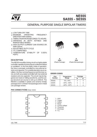
  • 1. July 1998 ® N DIP8 (Plastic Package) D SO8 (Plastic Micropackage) 1 2 3 4 5 6 7 8 1 - GND 2 - Trigger 3 - Output 4 - Reset 5 - Control voltage 6 - Threshold 7 - Discharge 8 - VCC PIN CONNECTIONS (top view) .LOW TURN OFF TIME .MAXIMUM OPERATING FREQUENCY GREATER THAN 500kHz .TIMING FROM MICROSECONDS TO HOURS .OPERATES IN BOTH ASTABLE AND MONOSTABLE MODES .HIGH OUTPUT CURRENT CAN SOURCE OR SINK 200mA .ADJUSTABLE DUTY CYCLE .TTL COMPATIBLE .TEMPERATURE STABILITY OF 0.005% PERo C ORDER CODES Part Number Temperature Range Package N D NE555 0o C, 70o C • • SA555 –40o C, 105o C • • SE555 –55 o C, 125 o C • • DESCRIPTION The NE555monolithictiming circuitisa highlystable controllercapableofproducingaccuratetime delays or oscillation. In the time delay mode of operation, the time is precisely controlled by one external re- sistorandcapacitor.Forastableoperationasanos- cillator, the free running frequency and the duty cy- cle are both accurately controlled with two external resistors and one capacitor.The circuit may be trig- gered and reset on falling waveforms, and the out- put structure can source or sink up to 200mA. The NE555 is available in plastic and ceramic minidip packageand in a 8-lead micropackage and inmetal can package version. NE555 SA555 - SE555 GENERAL PURPOSE SINGLE BIPOLAR TIMERS 1/10
  • 2. THRESHOLD COMP 5kΩ 5kΩ 5kΩ TRIGGER R FLIP-FLOP S Q DISCHARGE OUT INHIBIT/ RESET RESET COMP S - 8086 S + CONTROL VOLTAGE VCC BLOCK DIAGRAM OUTPUT CONTROL VOLTAGE THRESHOLD COMPARATOR VCC R1 4.7kΩ R2 830Ω Q5 Q6 Q7 Q8 Q9 R3 4.7kΩ R4 1kΩ R8 5kΩ Q1 Q2 Q3 Q4 Q10 Q11 Q12 Q13 THRESHOLD TRIGGER RES ET DISCHARGE G N D 2 4 7 1 Q14 Q15 R5 10kΩ R6 100kΩ R7 100kΩ R10 5kΩ Q17 Q16 Q18 R9 5kΩ D2 R16 100Ω R15 4.7kΩ R14 220Ω Q24 Q23 R17 4.7kΩ 3 Q22 Ρ13 D1 Q19 Q20 Q21 R12 6.8kΩ 5 TRIGGER COMPARATOR FLIP FLOP R11 5kΩ 3.9kΩ SCHEMATIC DIAGRAM ABSOLUTE MAXIMUM RATINGS Symbol Parameter Value Unit Vcc Supply Voltage 18 V Toper Operating Free Air Temperature Range for NE555 for SA555 for SE555 0 to 70 –40 to 105 –55 to 125 o C Tj Junction Temperature 150 o C Tstg Storage Temperature Range –65 to 150 o C NE555/SA555/SE555 2/10
  • 3. ELECTRICAL CHARACTERISTICS Tamb = +25o C, VCC = +5V to +15V (unless otherwise specified) Symbol Parameter SE555 NE555 - SA555 Unit Min. Typ. Max. Min. Typ. Max. ICC Supply Current (RL ∞) (- note 1) Low State VCC = +5V VCC = +15V High State VCC = 5V 3 10 2 5 12 3 10 2 6 15 mA Timing Error (monostable) (RA = 2k to 100kΩ, C = 0.1µF) Initial Accuracy - (note 2) Drift with Temperature Drift with Supply Voltage 0.5 30 0.05 2 100 0.2 1 50 0.1 3 0.5 % ppm/°C %/V Timing Error (astable) (RA, RB = 1kΩ to 100kΩ, C = 0.1µF, VCC = +15V) Initial Accuracy - (note 2) Drift with Temperature Drift with Supply Voltage 1.5 90 0.15 2.25 150 0.3 % ppm/°C %/V VCL Control Voltage level VCC = +15V VCC = +5V 9.6 2.9 10 3.33 10.4 3.8 9 2.6 10 3.33 11 4 V Vth Threshold Voltage VCC = +15V VCC = +5V 9.4 2.7 10 3.33 10.6 4 8.8 2.4 10 3.33 11.2 4.2 V Ith Threshold Current - (note 3) 0.1 0.25 0.1 0.25 µA Vtrig Trigger Voltage VCC = +15V VCC = +5V 4.8 1.45 5 1.67 5.2 1.9 4.5 1.1 5 1.67 5.6 2.2 V Itrig Trigger Current (Vtrig = 0V) 0.5 0.9 0.5 2.0 µA Vreset Reset Voltage - (note 4) 0.4 0.7 1 0.4 0.7 1 V Ireset Reset Current Vreset = +0.4V Vreset = 0V 0.1 0.4 0.4 1 0.1 0.4 0.4 1.5 mA VOL Low Level Output Voltage VCC = +15V, IO(sink) = 10mA IO(sink) = 50mA IO(sink) = 100mA IO(sink) = 200mA VCC = +5V, IO(sink) = 8mA IO(sink) = 5mA 0.1 0.4 2 2.5 0.1 0.05 0.15 0.5 2.2 0.25 0.2 0.1 0.4 2 2.5 0.3 0.25 0.25 0.75 2.5 0.4 0.35 V VOH High Level Output Voltage VCC = +15V, IO(source) = 200mA IO(source) = 100mA VCC = +5V, IO(source) = 100mA 13 3 12.5 13.3 3.3 12.75 2.75 12.5 13.3 3.3 V Notes : 1. Supply current when output is high is typically 1mA less. 2. Tested at VCC = +5V and VCC = +15V. 3. This will determine the maximum value of RA + RB for +15V operation the max total is R = 20MΩ and for 5V operation the max total R = 3.5MΩ. OPERATING CONDITIONS Symbol Parameter SE555 NE555 - SA555 Unit VCC Supply Voltage 4.5 to 18 4.5 to 18 V Vth, Vtrig, Vcl, Vreset Maximum Input Voltage VCC VCC V NE555/SA555/SE555 3/10
  • 4. ELECTRICAL CHARACTERISTICS (continued) Symbol Parameter SE555 NE555 - SA555 Unit Min. Typ. Max. Min. Typ. Max. Idis(off) Discharge Pin Leakage Current (output high) (Vdis = 10V) 20 100 20 100 nA Vdis(sat) Discharge pin Saturation Voltage (output low) - (note 5) VCC = +15V, Idis = 15mA VCC = +5V, Idis = 4.5mA 180 80 480 200 180 80 480 200 mV tr tf Output Rise Time Output Fall Time 100 100 200 200 100 100 300 300 ns toff Turn off Time - (note 6) (Vreset = VCC) 0.5 0.5 µs Notes : 5. No protection against excessive Pin 7 current is necessary, providing the package dissipation rating will not be exceeded. 6. Time mesaured from a positive going input pulse from 0 to 0.8x VCC into the threshold to the drop from high to low of the output trigger is tied to treshold. Figure 1 : Minimum Pulse Width Required for Trigering Figure 2 : Supply Current versus SupplyVoltage Figure 3 : Delay Time versus Temperature Figure 4 : Low Output Voltage versus Output Sink Current NE555/SA555/SE555 4/10
  • 5. Figure 5 : Low Output Voltage versus Output Sink Current Figure 6 : Low Output Voltage versus Output Sink Current Figure 7 : High Output Voltage Drop versus Output Figure 8 : Delay Time versus Supply Voltage Figure 9 : PropagationDelay versus Voltage Level of Trigger Value NE555/SA555/SE555 5/10
  • 6. CAPACITOR VOLTAGE = 2.0V/div t = 0.1 ms / div INPUT = 2.0V/div OUTPUT VOLTAGE = 5.0V/div R1 = 9.1kΩ, C1 = 0.01µF, R = 1kΩL Figure 11 Reset Trigger Output R1 C1 Control Voltage 0.01µF NE555 = 5 to 15VVCC 4 2 3 1 5 6 7 8 Figure 10 C (µF) 10 1.0 0.1 0.01 0.001 10 100 1.0 10 100 10 (t )d µs µs ms ms ms s 10M Ω 1M Ω 100kΩ 10kΩ R 1= 1kΩ Figure 12 APPLICATION INFORMATION MONOSTABLE OPERATION In the monostable mode, the timer functions as a one-shot.Referring to figure 10 the external capaci- tor is initially held discharged by a transistorinside the timer. The circuit triggers on a negative-goinginput signal when thelevel reaches1/3 Vcc. Once triggered,the circuit remains in this state until the set time has elapsed, even if it is triggered again during this in- terval.The durationof theoutputHIGHstateisgiven by t = 1.1 R1C1 and is easily determined by figure 12. Notice that since the charge rate and the threshold levelof the comparatorarebothdirectlyproportional to supply voltage, the timing intervalis independent of supply. Applying a negativepulse simultaneously to the reset terminal (pin 4) and the trigger terminal (pin 2) during the timing cycle discharges the exter- nalcapacitorand causesthe cycleto start over.The timing cycle now starts on the positive edge of the reset pulse. During the time the reset pulse in ap- plied, the output is driven to its LOW state. When a negativetriggerpulse is appliedtopin 2, the flip-flop is set, releasing the short circuit across the externalcapacitor anddriving the outputHIGH. The voltage across the capacitor increases exponen- tially with the time constantτ =R1C1. When the volt- ageacross the capacitorequals2/3 Vcc, the compa- ratorresetsthe flip-flop which thendischargethe ca- pacitor rapidly and drivers the output to its LOW state. Figure 11shows theactual waveforms generatedin this mode of operation. When Reset is not used, it should be tied high to avoid any possibly or false triggering. ASTABLE OPERATION When the circuit is connected as shown in figure 13 (pin 2and 6 connected)ittriggersitself andfreeruns as a multivibrator. The external capacitor charges through R1 and R2 and discharges through R2 only. Thus the dutycycle may beprecisely set bythe ratio of these two resistors. In the astable mode of operation, C1 charges and dischargesbetween 1/3 Vcc and 2/3 Vcc. As in the triggeredmode,thechargeanddischarge timesand therefore frequency are independentof the supply voltage. NE555/SA555/SE555 6/10
  • 7. t = 0.5 ms / div OUTPUT VOLTAGE = 5.0V/div CAPACITOR VOLTAGE = 1.0V/div R1 = R2 = 4.8kΩ, C1= 0.1µF, R = 1kΩL Figure 14 C (µF) 10 1.0 0.1 0.01 0.001 0.1 1 10 100 1k 10k f (Hz)o 1M Ω R1 + R2 = 10M Ω 100kΩ 10kΩ 1kΩ Figure 15 : Free Running Frequency versus R1, R2 and C1 Figure 14showsactualwaveformsgeneratedin this mode of operation. The charge time (output HIGH) is given by : t1 = 0.693 (R1 + R2) C1 and the discharge time (outputLOW) by : t2 = 0.693 (R2) C1 Thus the total period T is given by : T = t1 + t2 = 0.693 (R1 + 2R2) C1 The frequency ofoscillation is them : f = 1 T = 1.44 (R1 + 2R2) C1 and may be easily found by figure 15. The duty cycle is given by : D = R2 R1 + 2R2 Output 3 4 8 7 5 1 R1 C12 6 R2 Control Voltage NE555 VCC = 5 to 15V 0.01µF Figure 13 PULSE WIDTH MODULATOR When the timer is connected in the monostable mode and triggered with a continuous pulse train, theoutputpulse width can be modulatedby a signal applied to pin 5. Figure 16 shows the circuit. Trigger Output R C NE555 2 4 3 1 5 6 7 Modulation Input 8 A VCC Figure 16 : Pulse Width Modulator. NE555/SA555/SE555 7/10
  • 8. LINEAR RAMP When the pullup resistor, RA, in the monostablecir- cuitis replacedbya constantcurrentsource,alinear ramp is generated. Figure 17 shows a circuit con- figuration that will perform this function. Trigger Output C NE555 2 4 3 1 5 6 7 8 E VCC 0.01µF R2 R1R 2N4250 or equiv. Figure 17. Out RA C NE55 2 4 3 1 5 6 7 8 VCC 51kΩ RB 22kΩ 0.01µF VCC 0.01µF Figure 19 : 50%Duty Cycle Oscillator. Figure 18 shows waveformsgeneratorby the linear ramp. The time interval is given by : T = (2/3 VCC RE (R1+ R2) C R1 VCC − VBE (R1+ R2) VBE = 0.6V Figure 18 : Linear Ramp. VCC = 5V Top trace : input 3V/DIV Time = 20µs/DIV Middle trace : output 5V/DIV R1 = 47kΩ Bottom trace : output 5V/DIV R2 = 100kΩ Bottom trace : capacitor voltage RE = 2.7kΩ 1V/DIV C = 0.01µF 50% DUTY CYCLE OSCILLATOR For a 50% duty cycle the resistors RA and RE may beconnectedasin figure19.Thetime preriodforthe output high is the same as previous, t1 = 0.693 RA C. For the output low it is t2 = [(RARB) ⁄ (RA + RB)] CLn    RB − 2RA 2RB − RA    Thus the frequencyof oscillation is f = 1 t1 + t2 Note that this circuit will not oscillate if RB is greater than 1/2 RA because the junction of RA and RB can- notbring pin2 down to 1/3 VCC andtriggerthelower comparator. ADDITIONAL INFORMATION Adequate power supply bypassing is necessary to protect associated circuitry. Minimum recom- mended is 0.1µF in parallel with 1µF electrolytic. NE555/SA555/SE555 8/10
  • 9. PM-DIP8.EPS PACKAGE MECHANICAL DATA 8 PINS - PLASTIC DIP Dimensions Millimeters Inches Min. Typ. Max. Min. Typ. Max. A 3.32 0.131 a1 0.51 0.020 B 1.15 1.65 0.045 0.065 b 0.356 0.55 0.014 0.022 b1 0.204 0.304 0.008 0.012 D 10.92 0.430 E 7.95 9.75 0.313 0.384 e 2.54 0.100 e3 7.62 0.300 e4 7.62 0.300 F 6.6 0260 i 5.08 0.200 L 3.18 3.81 0.125 0.150 Z 1.52 0.060 DIP8.TBL NE555/SA555/SE555 9/10
  • 10. PM-SO8.EPS PACKAGE MECHANICAL DATA 8 PINS - PLASTIC MICROPACKAGE (SO) Dimensions Millimeters Inches Min. Typ. Max. Min. Typ. Max. A 1.75 0.069 a1 0.1 0.25 0.004 0.010 a2 1.65 0.065 a3 0.65 0.85 0.026 0.033 b 0.35 0.48 0.014 0.019 b1 0.19 0.25 0.007 0.010 C 0.25 0.5 0.010 0.020 c1 45 o (typ.) D 4.8 5.0 0.189 0.197 E 5.8 6.2 0.228 0.244 e 1.27 0.050 e3 3.81 0.150 F 3.8 4.0 0.150 0.157 L 0.4 1.27 0.016 0.050 M 0.6 0.024 S 8 o (max.) SO8.TBL Information furnished is believed to be accurate and reliable. However, STMicroelectronics assumes no responsibility for the consequences of use of such information nor for any infringement of patents or other rights of third parties which may result from its use. No license is granted by implication or otherwise under any patent or patent rights of STMicroelectronics. Specifi- cations mentioned in this publication are subject to change without notice. This publication supersedes and replaces all infor- mation previously supplied. STMicroelectronics products are not authorized for use as critical components in life support devices or systems without express written approval of STMicroelectronics. © The ST logo is a trademark of STMicroelectronics © 1998 STMicroelectronics – Printed in Italy – All Rights Reserved STMicroelectronics GROUP OF COMPANIES Australia - Brazil - Canada - China - France - Germany - Italy - Japan - Korea - Malaysia - Malta - Mexico - Morocco The Netherlands - Singapore - Spain - Sweden - Switzerland - Taiwan - Thailand - United Kingdo m- U.S.A. ORDERCODE: NE555/SA555/SE555 10/10