Download to read offline
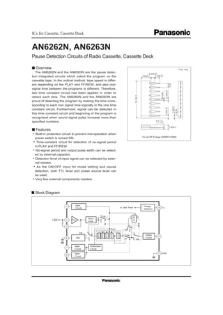

The AN6262N and AN6263N are integrated circuits that detect pauses in cassette tapes during playback and fast forward/rewind modes. They use a single time constant circuit to detect the non-signal time between programs, rather than using different time constants for different tape speeds. The circuits output a detection signal when the non-signal time exceeds a duration determined by an external capacitor. They can detect program signals and ignore noise by counting the number of signal pulses. External components are minimal, with only a capacitor needed to set the non-signal detection time.