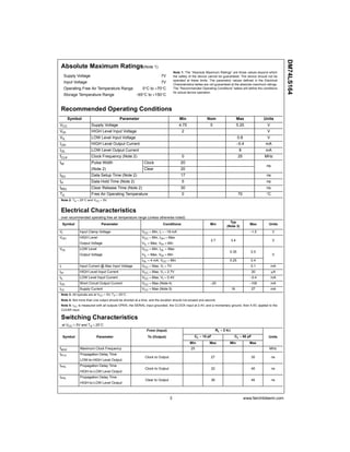
Download to read offline
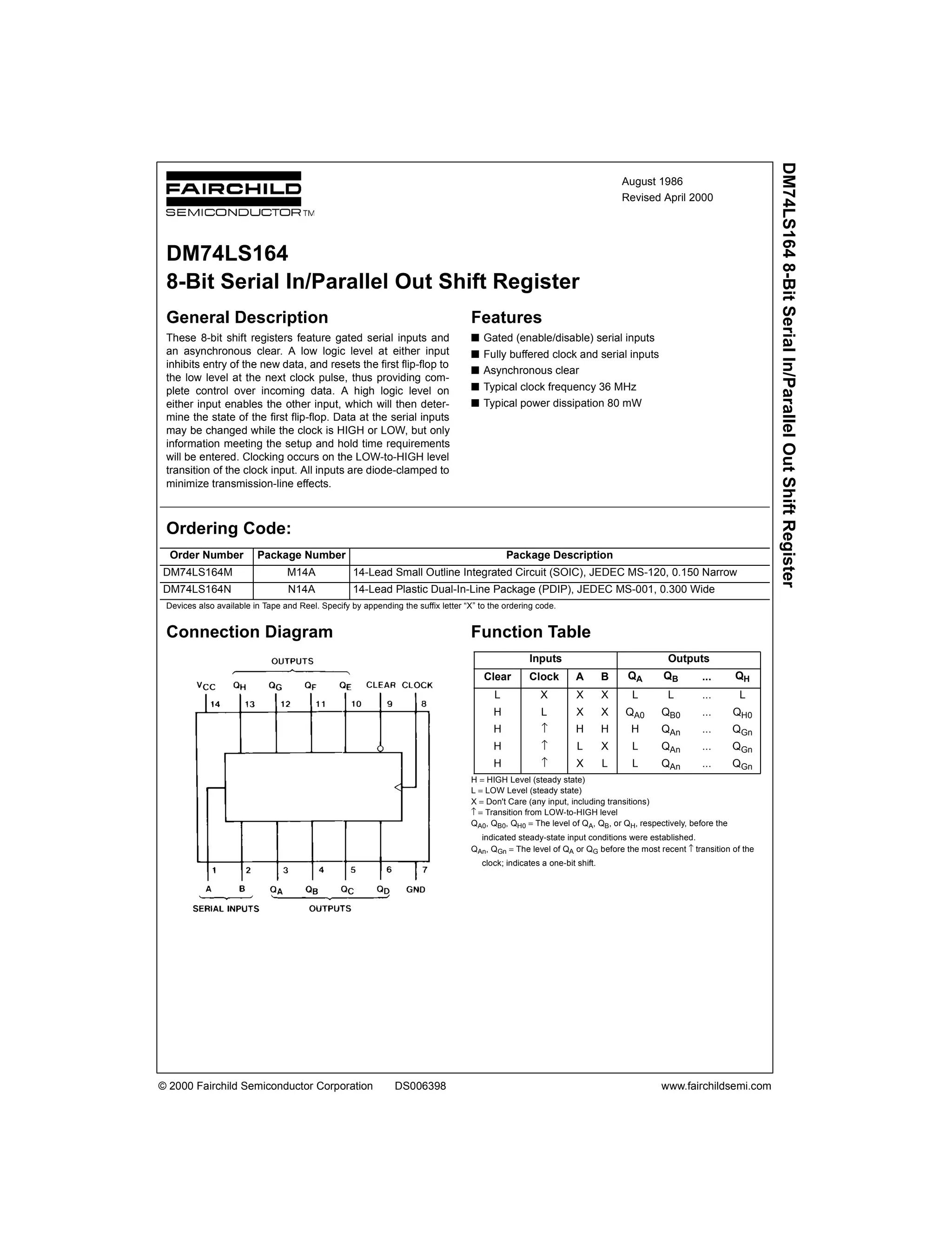
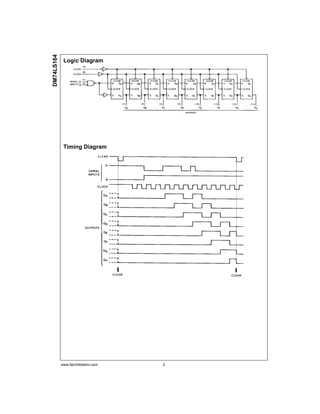
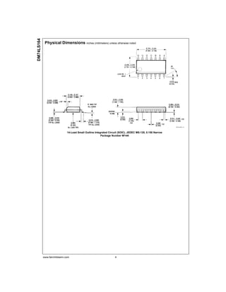
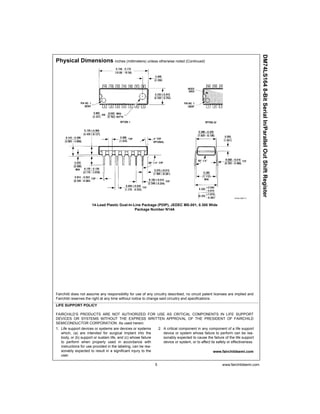
This document provides information on the DM74LS164 8-Bit Serial In/Parallel Out Shift Register integrated circuit from Fairchild Semiconductor. It has gated serial inputs, asynchronous clear, fully buffered clock and inputs, and can operate at clock frequencies up to 36 MHz while dissipating around 80 mW of power. The device is available in either a 14-pin Small Outline Integrated Circuit package or a 14-pin Plastic Dual-In-Line package. Electrical characteristics, switching characteristics, and physical dimension drawings are also included.