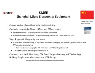
The Semiconductor Industry
Steve Blank
sblank@kandranch.com
V7 092021
Gordian Knot Center for
National Security Innovation
Table of Contents
• Slides 3 -15 Semi Industry Overview
• Slides 16 - 20 Trusted Foundry Program
• Slides 21 - 37 Glossary and Sources
• Slides 38 - 50 China Semi Industry Overview
• Slides 51 - 76 China Foundries
• Slides 7 7- 86 China IDMs
• Slides 87 - 98 China Fabless
• Slides 99 - 114 Fab construction 101
• Slides 115 - 198 Wafer Fab Equipment China
• Slides 199 - 208 China Wafer Fab Equipment Needs
• Slides 209-214 China Semi Acquisitions
• Slides 215 - 226 Power Semiconductors
• Slides 227 – 236 RF semiconductors
• Slides 237-247 TSMC Fabs
Companies and Governments
That Use Chips in Systems
End Products
Semiconductor
Ecosystem
Chip Intellectual Property (IP) Cores
• The design of a chip may be owned by a single company, or…
• Some companies license their chip designs -as building blocks
– called IP Cores - for wide use
Chip IP Cores
Electronic Design Automation (EDA) Tools
Electronic Design
Automation Tools
• Engineers design chips using specialized EDA software
• The industry is dominated by three U.S. vendors
Chip Manufacturing Needs Specialized Materials
Materials and
Subsystems
• Silicon wafers, crystal growing furnaces
• Gases & fluids (Fluorine, Argon, Helium, Arsine, Phosphine, diboron...)
• Photomasks and resists, top coats, CMP slurries
• Wafer handling equipment, dicing
• RF Power equipment
Wafer Fab Equipment (WFE) Make the Chips
Wafer Fab
Equipment
• These are the machines that manufacture the chips
• Five companies dominate the industry - Applied, KLA, LAM, TEL, ASML
• ASML - a Dutch company - supplies the most advanced
lithography (EUV)
“Fabless” Chip Companies
Fabless chip
companies
• They create chip designs and send the designs to
“foundries” (aka “fabs”) that manufacture them
• They do not own Wafer Fab Equipment
• They do use Chip IP and Electronic Design Software
• They may use the chips
exclusively in their own devices
e.g. Apple, Nvidia….
• Or they may sell the chips to
everyone e.g. AMD, Qualcomm…
Integrated Device Manufacturers (IDMs)
Integrated Device
Manufacturers
(IDMs)
• IDMs design, manufacture, and sell chips
• Three categories – Memory (e.g. Micron), Logic (e.g. Intel), Analog (Analog Devices)
• They have their own “fabs” but may also use foundries
Chip Foundries • Foundries make chips for others
• They buy and integrate equipment
from a variety of manufacturers
• They design unique processes using
this equipment to make the chips
• But they don’t design chips
• TSMC in Taiwan is the leader in logic
Think of a Fab as Analogous to a Printing Plant
Foundries and IDMs have Fabs
Book Printing Chip Fabrication
An author writes a book
They use a word processor
An engineer designs a chip
They use EDA Tools
They contract with a publisher who
sends text to the printing plant
It may print novels, tech manuals, histories, etc.
They select a Fab appropriate for their
type of Chip
Memory, logic, RF, analog
The plant buys raw materials
Paper, ink
The fab buys raw materials
Silicon, chemicals, gases
The plant buys printing machinery
printing presses, binding, trimming
The fab buys wafer fab equipment
Etchers, deposition, lithography, testers, packaging
The printing process - offset
lithography
Filming, stripping, blueprints, plate making,
printing, binding, trim
Chip manufacturing process - offset
lithography
Etching, diffusion, lithography, assembly, testing,
packaging
The plant turns out millions of copies The plant turns out millions of copies
(Then think of its complexity as a continuous industrial processes like Oil & Gas, Chemical Reactors, uranium enrichment)
The Flow - From an Idea to Silicon
System
Specification
Architectural
Design
Functional &
Logic Design
Circuit
Design
Physical
Design
Physical
Verification
Layout Data
(GDSII, OASIS)
Mask Data
Prep
Design Engineers at Fabless or IDMs Using Electronic Design Automation Software
Package and
Test Chips
Fabricate
Chips
Mask in Litho
System
Create Mask
Blank
Write Pattern
on Blank
At
Photomask
Maker
Create Mask
Set
Create
Pellicle
In the Fab
Three Types of Chip
Factories (“Fabs”)
Chip
manufacturers
Foundries
IDMs
Air Liquide, Linde, Cabot, JSR, MKS,UCTT,
Ichor, Brooks, Jabil, Celestica, Dow Advanced Energy
Wafers: Shin-Etsu, Sumco, GlobalWafer, Siltronic, SK Siltron
They design the chips into products for
consumers, companies and military systems
Companies buy chips
from Foundries and IDMs
Air Liquide, Linde, Cabot, JSR, MKS,UCTT,
Ichor, Brooks, Jabil, Celestica, Dow Advanced Energy
Wafers: Shin-Etsu, Sumco, GlobalWafer, Siltronic, SK Siltron
Products are Sold to End
Customers – Military and Civilian
End Products
• iPhones
• AI/ML
• Datacenters
• Networking (5G)
• Weapons
• …
DoD Trusted Foundry program
• DMEA is the program manager for the DoD Trusted Foundry program
• Provide an assured "Chain of Custody" for both classified and
unclassified ICs
• Ensure that there will not be any reasonable threats related to
disruption in supply
• Prevent intentional or unintentional modification or tampering of the ICs
• Protect the ICs from unauthorized attempts at reverse engineering,
exposure of functionality or evaluation of their possible vulnerabilities
The Trusted Access Program Office (TAPO)
• Facilitates and administers the contracts and agreements with
industry to provide US Government users with:
• Leading edge foundry services including multi-project wafer runs,
dedicated prototypes, and production in both high- and low-volume
models
• A library of standard IP blocks
• Limited packaging and test services
Trusted Foundries
• BAE Systems
• CREE
• Defense Microelectronics Agency
• Global Foundries
• HRL Labs
• M/A-Com
• MIT Lincoln Labs
• Northrup Grumman
• ON Semiconductor
• Quovro
• Raytheon
• Sandia
• Skywater Technology
• SRI
• TSI Semiconductors
As of May 2021
https://www.dmea.osd.mil/otherdocs/accreditedsuppliers.pdf
Trusted Technology Portfolio
Semi Industry
Extra Info
Steve Blank
sblank@kandranch.com
V3 071121
29 New Fabs Starting Construction in 2021-22
• 15 are foundries with capacities ranging from 30,000 to 220,000 200mm equivalent wafers
per month
• 4 are for memory chips with capacities of 100,000 to 400,000 200mm equivalent wafers per
month
Glossary -1
• APT (assembly, packaging, and test)
• CAPEX (capital equipment expense) dollars spent on new equipment and buildings
• CIS (CMOS image sensor)
• Die unpackaged, bare square of silicon containing an integrated circuit that has been cut
out of the wafer
• EDA (electronic design automation) software tools engineers use to design chips
• Fab is a factory that manufacturers chips
• Fabless companies create chip designs and send them to “foundries” that manufacture
them
• Foundries manufactures (fabs) chips for others
• IDM (integrated device manufacturer) designs, fabs, and sells their own chips (logic,
memory, power, etc.)
• Logic Devices – chips that do computing; microprocessors, microcontrollers, GPU’s,
ASICs,
Glossary - 2
• OSAT (outsourced semiconductor assembly & testing)
• Lithography stencils patterns of integrated circuits onto silicon wafers
• Memory Devices store information – DRAM and Flash memory
• MEMS (micro-electromechanical system) sensors and actuators
• Nanometer (nm) – one billionth of an inch
• Nodes (technology node, process node, process technology) a specific manufacturing
process and its design rules. Nodes 14nm, 10nm, 7nm, 5nm refer to a generation of chips
made in a particular technology. The smaller the node the more transistors can fit on a
wafer.
• Wafer the silicon substrate used to make chips
• Wafer Size: diameter of the silicon wafer used in manufacturing currently modern fabs
are ~8” 200mm or ~12” 300mm
• WPM (wafers per month) a measurement of the output of a fab
Glossary 3– Fab Processes
• Bunny Suit garment worn in a cleanroom to prevent skin and hair from
contaminating the chip process
• Chemical mechanical planarization (CMP) removes excess material on the wafer’s
front surface and flattens the wafer
• Cleanroom -specially constructed, enclosed spaces where chips are made. Classed
by the # of particles per cubic foot
• Diffusion (sometimes referred to as annealing) is a thermal treatment used to
move dopants, or impurities, and make dopants introduced by ion implantation
electrically active
• Doping intentional introduction of impurities to change its electrical, properties
• ion implantation is the most important doping method. Ions (positively or negatively charged
atoms) of dopant chemicals (boron, arsenic, etc.) are accelerated in an electrical field and
impacted into a wafer to penetrate its surface, changing the electrical characteristics of the
material
Glossary 4– Fab Processes
• Epitaxy (deposition) deposits a layer of material (conductor, insulator or
semiconductor) on a silicon wafer. The process can be repeated 40-100 times on a
single wafer. There are different types of deposition processes:
• Atomic Layer Deposition (ALD) layer-by-layer process that results in the deposition of thin
films one atomic layer at a time
• Chemical vapor deposition (CVD): deposits gaseous material onto the wafer in solid form (e.g.,
silicon dioxide, polysilicon) which react and/or decompose on the substrate surface through a
high-temperature (500-900 degrees Celsius) process
• Metal Organic Chemical Vapor Deposition (MOCVD) used in chip production of made from
materials other than silicon (Gallium Nitride and Gallium Arsenide), LEDs, laser diodes,
photonic chips, power/RF devices for radar, electronic warfare, communications and solar cells
• Plasma-enhanced CVD (PECVD): is a variation of CVD using ionizing gases but does not require
a high-temperature environment and is ideal for film deposition after the initial metal
deposition without disturbing the existing metal layer
• Oxidation: converts existing silicon into silicon dioxide (with the help of oxygen) in a furnace.
Silicon dioxide is an insulator
• Physical vapor deposition (PVD): Also called “sputtering”, uses physical/plasma bombardment
of source material that releases atoms for deposit on the wafer surface and usually relates to
metal deposition
Glossary 5– Fab Processes
• Etching A process for removing material
• Dry etching - under vacuum (dry) typically using a plasma to generate gas-
phase reactants.
• liquid-phase (wet) etchants *sulfuric acid, nitric acid, phosphoric acid, or
hydrofluoric acid)
• Low Pressure Chemical Vapor Deposition (LPCVD) is a thermal process
that deposits various films at low pressure
• NA numerical aperture - a number that characterizes the range of
angles over which the system can accept or emit light
• OSAT (outsourced semiconductor assembly & testing)
• Photomask contains the pattern of an integrated circuit
Logic Chips
These do Computing
• High-end CPUs – microprocessors, microcontrollers, e.g. Intel x86
• U.S.: Intel, AMD
• China: Loongson, Zhaoxin, Sunway, Phytium
• GPUs (Graphic Processing Units) – used for AI,/ML, Bitcoin, graphics
• U.S.: Nvidia , AMD
• China: Jingjia Micro
• FPGAs (Field Programable Gate Arrays) – reprogrammable processors
• U.S.: Xilinx, Intel, Lattice, Microchip, Achronix.Flex Logic
• China: Efinix, Gowin, Shenzhen Pango
• AI ASICs (Application Specific ICs) – run specific AI algorithms
• U.S.: Google, Facebook, Cerebras, Tesla (U.S.),
• China: HiSilicon. Cambricon, Horizon Robotics , Intellifusion , …
Memory Chips
These store information
• DRAM Memory chips – requires power to store data
• Samsung (South Korea), SK Hynix (South Korea), Micron (U.S.), Nanya
(Taiwan), Winbond (Taiwan), Powerchip (Taiwan), ChangXin (China)
• NAND Flash – retains data when power is off
• Samsung (South Korea), Toshiba (Japan), Western Digital (U.S.), Micron (U.S.),
Intel (U.S.), SK Hynix (South Korea), YMTC (China)
Who Are IDMs? (1)
• Logic chips – microprocessors, microcontrollers, e.g. Intel x86
• Intel (U.S.), Renesas (Japan), STMicroelectronics (Switzerland), Microchip
(U.S.), NXP (U.S./Netherlands), Toshiba (Japan), …
• Memory Chips – stores data
• SK Hynix (South Korea), Samsung (South Korea), Micron (U.S.), Toshiba
(Japan), Western Digital (U.S.), Intel (U.S.), YMTC (China), ChangXin (China),…
• Analog Chips
• Texas Instruments (U.S.), ON (U.S.), SiEn (China), ASMC (China), Bosch
(Germany), STMicroelectronics (Switzerland), TowerJazz (Japan), ….
| Applied Materials Confidential
19
Semiconductor Ecosystem
Wafer Fab Materials & Subsystems
Wafer Fab Equipment
Who Are IDMs?(2)
• Optoelectronics Chips
• Sony (Japan), Nichia (Japan), Samsung (South Korea), Osram (Germany),
HC SemiTek (China), Epistar (Taiwan), Sanan (China), Aucksun (China),
Changelight (China), …
• Sensors
• Qorvo (U.S.), Broadcom (U.S.), Seagate (U.S.), Texas Instruments (U.S.),
OmniVision (China), SMIC (China),
• Discrete Chips - Infineon (Germany), STMicroelectronics
• (Switzerland), Hangzhou (China), ON (U.S.), Mitsubishi (Japan), AOS (U.S.),
CR (China), Yangzhou (China),
| Applied Materials Confidential
19
Semiconductor Ecosystem
Wafer Fab Materials & Subsystems
Wafer Fab Equipment
IDM/Foundry Logic Node Roadmap
Global
Foundries
Only 2 Foundries Are At the Leading Edge Node
 
2003
17
90nm
2001
17
130nm
2005
14
65nm
2007
12
45nm 2009
9
32nm 2012
6
22nm
2015
4
14nm
2017
3
10nm
2020
2
7nm
Year in Production
# of Companies
Node
Does Node Size Matter?
• While SMIC and HSMC’s 14nm technology lags behind TSMC’s 5nm
capability, there is nothing computationally a 5nm chip can do that a
14nm chip cannot do
• The key difference, is that the 14nm chip is bigger, uses up more
silicon and may consume more power relative to its performance
• In cases where its size is not a major constraint, e.g. data centers,
autonomous vehicles, big data and AI in cloud computing, China has
what it already needs
• However, these foundries won’t be able to deliver high-end, high-
performance chips that will go into, the newest 5G-smartphones or
drone
Shrinking Nodes – Why Is It Important?
cost per die will fall after production yields reach pre-(size)-transition levels.
The figure below illustrates the effects of theoretical wafer linewidth shrinkage.
When linewidth halves from 0.5 microns to 0.25 microns, the wafer can
theoretically hold a quadrupled (22) number of dies. In terms of cost savings, a
quadrupled number of dies would lead to a 75% per-DRAM cost reduction in a
typical 300mm DRAM wafer, excluding additional mask and depreciation costs.
Figure 48: Illustration of wafer linewidth shrinkage
Source: Deutsche Bank
Smaller die sizes also improve production yields (i.e., the number of acceptable,
functional dies as a percentage of total dies on a wafer) as smaller dies
are less susceptible to contaminations during manufacturing (given a static
amount of contamination, the smaller the die size, the lower the probability that
contamination will affect a die). Companies typically reduce contamination and
improve yield through manufacturing environment control, employee training,
• Can put more dies (chips)
on the same size wafer =
lower cost
• Can put more transistors
on one chip = making
them more complex
Readings/Sources
Center For Security and Emerging Technology - read all the semi papers
Semiconductor Manufacturing Handbook - Hwaiyu Geng
Credit Suisse - read all the analyst reports on semiconductors
Goldman Sachs - read all the analyst reports on semiconductors
Financial Times - read all the China articles on semiconductors
Brookings Institute - read semi report
Congressional Research Service - Michaela Platzer, John Sargent
SEMI – Fab Construction Monitor Database
Semi Analysts – Sources
*** Saif M. Khan Director for Tech & National Security at National Security Council. ***
Credit Suisse China Semi Analysts: Randy Abrams, Chaolien Tseng , John W. Pitzer
Goldman Sachs China Semi Analysts: Allen Chang, Jin Guo, Lynn Luo, Verena Jeng
Center For Security and Emerging Technology - James Lewis, Alexander Mann , Dahlia Peterson ,
Carrick Flynn
Bernstein China Semi Analysts: Mark Li, Hanxu Wang, Edward Hou, Power/RF: Stacy A. Rasgon
KKR - Vance Serchuk
Brookings Institute Christopher A. Thomas
Financial Times China Semi Reporters: Cheng Ting-Fang and Lauly Li, Nikkei Staff Writers
Accenture China Semi Analysts: Syed Alam, Sam Baker
Congressional Research Service - Michaela Platzer - John Sargent
Nomura China Semi Analysts: Donnie Teng, Aaron Jeng
Jefferies China Semi Analyst: Mark Lipacis
China’s Chip Ecosystem
Semiconductors Are China’s Biggest Imports
2020 Trade Balance
More Than Oil
China Semi Status
• Success in LEDs, low-power processors, sensors, discrete
semiconductor devices, and in assembly, packaging, and test (APT)
• Behind in multi-core processors and memory devices, semiconductor
design tools and equipment, especially at the smaller, leading-edge
process nodes
• Lags somewhat in analog / mixed signal ICs and RF (radio frequency)
front-end components for cellphones such as power amplifiers and RF
filters
• Full self-sufficiency in all of these will require China to produce even
more advanced semiconductor equipment than what is required at
the 28 nm CMOS node
China National IC Fund Fuels Their Ecosystem
20 January 2021
Figure 47: China IC fund major semiconducto
Source: Company data, Credit Suisse estimates
In addition to the listed companies, the National IC
private companies in China. We believe these highe
strategic sectors including foundry (SMIC fab JVs,
Kingston’s Payton back-end subsidiary), equipmen
Priced 1/13/21 Company
Listed companies Ticker Description 03
NSIG 688126.SS Bare Wafer 5
AMEC 688012.SS Semi equipment
SMIC 0981.HK Foundry 7
JCET 600584.SS Back-end 3
Sanan 600703.SS LED/RF Foundry 4
Naura 002371.SZ Semi Equipment
Hua Hong 1347.HK Foundry 2
Gigadevice 603986.SS MCU/NOR
Tongfu 002156.SZ Back-end 2
CR Micro 688396.SS Analog/Foundry
Goodix 603160.SS Sensor & Touch IC
BDStar Navigation 002151.SZ GPS ICs/Modules 5
Verisilicon 688521.SS IP & Design Service
WLCSP 603005.SS Back-end
Sai Microelectronics 300456.SZ MEMs/GaN Process
Jingjia Micro 300474.SZ GPUs
Anji Micro 688019.SS CMP/Resist
Yoke Technology 002409.SZ Semi/Display Material
Rockchip 603893.SS Consumer/IoT APs
Ingenic 300223.SZ MCU, video, memory
Hangzhou Changchuan 300604.SZ IC Test
Goke Micro 300672.SZ STB, SSD, IoT SOCs 2
Wanye 600641.SS Inv. Fund / Ion Implant
Wuxi Taiji Industry 600667.SS Back-end & Chem fiber 1
Ninestar 002180.SZ Printer/NFC ICs 3
Wuxi Chipown 688508.SS Analog and LED ICs
Wingtech 600745.SS ODM/Nexperia Analog
NavInfo 002405.SZ Auto map, service, ICs 1
3peak Incorporated 688536.SH Analog ICs
Expressif 688018.SS Wifi/Bluetooth ICs
Beken 603068.SS BT/Wifi/Audio ICs
Chipsea 688595.SS MCU, BT/Wifi ICs
Allwinner 300458.SZ Consumer/IoT APs
MEMSensing 688286.SS MEMs devices
20 January 2021
Figure 47: China IC fund major semiconductor holdings o
Source: Company data, Credit Suisse estimates
In addition to the listed companies, the National IC fund is also b
private companies in China. We believe these higher profile com
strategic sectors including foundry (SMIC fab JVs, Huali), memo
Kingston’s Payton back-end subsidiary), equipment (ACM), mob
Priced 1/13/21 Company
Listed companies Ticker Description 03/31/20 06/30/20
NSIG 688126.SS Bare Wafer 567.0 567.0
AMEC 688012.SS Semi equipment 93.3 93.3
SMIC 0981.HK Foundry 797.1 797.1
JCET 600584.SS Back-end 304.5 304.5
Sanan 600703.SS LED/RF Foundry 460.9 460.9
Naura 002371.SZ Semi Equipment 49.2 49.2
Hua Hong 1347.HK Foundry 242.4 242.4
Gigadevice 603986.SS MCU/NOR 30.0 39.2
Tongfu 002156.SZ Back-end 250.6 239.2
CR Micro 688396.SS Analog/Foundry 34.2 78.1
Goodix 603160.SS Sensor & Touch IC 25.6 25.6
BDStar Navigation 002151.SZ GPS ICs/Modules 58.8 58.8
Verisilicon 688521.SS IP & Design Service 34.7 34.7
WLCSP 603005.SS Back-end 21.7 27.1
Sai Microelectronics 300456.SZ MEMs/GaN Process 88.4 88.4
Jingjia Micro 300474.SZ GPUs 27.5 27.5
Anji Micro 688019.SS CMP/Resist 6.1 6.1
Yoke Technology 002409.SZ Semi/Display Material 26.5 26.5
Rockchip 603893.SS Consumer/IoT APs 25.9 25.9
Ingenic 300223.SZ MCU, video, memory 0.0 16.8
Hangzhou Changchuan 300604.SZ IC Test 31.0 31.0
Goke Micro 300672.SZ STB, SSD, IoT SOCs 26.3 26.3
Wanye 600641.SS Inv. Fund / Ion Implant 56.4 56.4
Wuxi Taiji Industry 600667.SS Back-end & Chem fiber 130.0 130.0
Ninestar 002180.SZ Printer/NFC ICs 32.1 32.1
Wuxi Chipown 688508.SS Analog and LED ICs 7.5 7.5
Wingtech 600745.SS ODM/Nexperia Analog 4.0 3.1
NavInfo 002405.SZ Auto map, service, ICs 13.2 13.2
3peak Incorporated 688536.SH Analog ICs 0.3 0.3
Expressif 688018.SS Wifi/Bluetooth ICs 1.2 1.2
Beken 603068.SS BT/Wifi/Audio ICs 1.4 1.4
Chipsea 688595.SS MCU, BT/Wifi ICs 1.2 1.2
Allwinner 300458.SZ Consumer/IoT APs 2.0 2.0
MEMSensing 688286.SS MEMs devices 0.4 0.4
Holding (s
China IC Fund
Public Chip
Companies
• a.k.a. the Big Fund or the China IC
Fund has invested directly or
indirectly in more than 60 China
chip companies
• $20 billion in 2014
• $29 billion in 2019
Global Semiconductors Sector 23
Figure 47: China IC fund major semiconductor holdings of listed companies, holdings trimmed on companies in orange and blue
Source: Company data, Credit Suisse estimates
In addition to the listed companies, the National IC fund is also backing a number of high profile
private companies in China. We believe these higher profile companies span many of the
strategic sectors including foundry (SMIC fab JVs, Huali), memory (YMTC, CXMT, Puya, and
Kingston’s Payton back-end subsidiary), equipment (ACM), mobile (UniSOC), and IoT (ApexMic,
KT, Bestechnic) and display/imaging (Galaxycore).
Figure 48: China IC fund holdings of high profile China private companies
Source: Company data, Credit Suisse
Priced 1/13/21 Company IC Fund Total 2020E Price/
Listed companies Ticker Description 03/31/20 06/30/20 09/30/20 12/04/20 03/31/20 06/30/20 09/30/20 12/04/20 Holding ($) Market cap Sales Sales
NSIG 688126.SS Bare Wafer 567.0 567.0 567.0 567.0 30.5% 22.9% 22.9% 22.9% $2,799 $12,243 $302 40.5
AMEC 688012.SS Semi equipment 93.3 93.3 93.3 93.3 17.5% 17.5% 17.5% 17.5% $2,282 $13,079 $361 36.3
SMIC 0981.HK Foundry 797.1 797.1 797.1 797.1 15.5% 14.0% 10.4% 10.4% $2,081 $20,099 $4,214 4.8
JCET 600584.SS Back-end 304.5 304.5 304.5 288.5 19.0% 19.0% 19.0% 18.0% $2,073 $11,516 $3,873 3.0
Sanan 600703.SS LED/RF Foundry 460.9 460.9 416.1 379.4 11.3% 11.3% 9.3% 8.5% $2,058 $24,297 $1,312 18.5
Naura 002371.SZ Semi Equipment 49.2 49.2 44.3 44.3 9.9% 9.9% 8.9% 8.9% $1,531 $17,168 $853 20.1
Hua Hong 1347.HK Foundry 242.4 242.4 242.4 242.4 18.8% 18.7% 18.7% 18.7% $1,331 $7,114 $951 7.5
Gigadevice 603986.SS MCU/NOR 30.0 39.2 34.5 34.5 9.3% 8.3% 7.3% 7.3% $1,151 $15,719 $708 22.2
Tongfu 002156.SZ Back-end 250.6 239.2 227.7 227.7 21.7% 20.7% 19.7% 17.1% $998 $5,827 $1,596 3.7
CR Micro 688396.SS Analog/Foundry 34.2 78.1 78.1 78.1 2.9% 6.4% 6.4% 6.4% $832 $12,942 $1,046 12.4
Goodix 603160.SS Sensor & Touch IC 25.6 25.6 21.3 21.1 5.6% 5.6% 4.7% 4.6% $517 $11,216 $1,098 10.2
BDStar Navigation 002151.SZ GPS ICs/Modules 58.8 58.8 49.0 49.0 12.0% 12.0% 9.6% 9.6% $401 $4,161 $544 7.7
Verisilicon 688521.SS IP & Design Service 34.7 34.7 34.7 34.7 8.0% 8.0% 7.2% 7.2% $374 $5,218 $252 20.7
WLCSP 603005.SS Back-end 21.7 27.1 27.1 27.1 9.4% 8.4% 8.4% 8.4% $332 $3,931 $188 20.9
Sai Microelectronics 300456.SZ MEMs/GaN Process 88.4 88.4 88.4 88.4 13.8% 13.8% 13.8% 13.8% $314 $2,268 $123 18.4
Jingjia Micro 300474.SZ GPUs 27.5 27.5 27.5 27.5 9.1% 9.1% 9.1% 9.1% $302 $3,306 $120 27.5
Anji Micro 688019.SS CMP/Resist 6.1 6.1 6.1 6.1 11.6% 11.6% 11.6% 11.6% $269 $2,329 $61 38.0
Yoke Technology 002409.SZ Semi/Display Material 26.5 26.5 26.5 26.5 5.7% 5.7% 5.7% 5.7% $267 $4,666 $419 11.1
Rockchip 603893.SS Consumer/IoT APs 25.9 25.9 25.9 25.9 6.3% 6.3% 6.3% 6.3% $252 $4,003 $278 14.4
Ingenic 300223.SZ MCU, video, memory 0.0 16.8 16.8 16.8 0.0% 3.7% 3.6% 3.6% $212 $5,904 $73 80.6
Hangzhou Changchuan 300604.SZ IC Test 31.0 31.0 31.0 31.0 9.9% 9.9% 9.9% 9.9% $180 $1,823 $120 15.2
Goke Micro 300672.SZ STB, SSD, IoT SOCs 26.3 26.3 26.3 26.3 14.6% 14.6% 14.6% 14.6% $177 $1,212 $113 10.7
Wanye 600641.SS Inv. Fund / Ion Implant 56.4 56.4 67.7 67.7 7.0% 7.0% 7.1% 7.1% $167 $2,357 $182 12.9
Wuxi Taiji Industry 600667.SS Back-end & Chem fiber 130.0 130.0 108.9 108.9 6.2% 6.2% 5.2% 5.2% $160 $3,087 $2,588 1.2
Ninestar 002180.SZ Printer/NFC ICs 32.1 32.1 32.1 32.1 3.0% 3.0% 3.0% 3.0% $128 $4,248 $3,120 1.4
Wuxi Chipown 688508.SS Analog and LED ICs 7.5 7.5 7.5 7.5 8.9% 8.9% 6.7% 6.7% $93 $1,400 $64 21.8
Wingtech 600745.SS ODM/Nexperia Analog 4.0 3.1 unknown unknown 0.4% 0.3% unknown unknown $61 $22,255 $9,977 2.2
NavInfo 002405.SZ Auto map, service, ICs 13.2 13.2 11.0 11.0 0.7% 0.7% 0.6% 0.6% $27 $4,758 $372 12.8
3peak Incorporated 688536.SH Analog ICs 0.3 0.3 unknown unknown 0.4% 0.4% unknown unknown $21 $4,893 $93 52.5
Expressif 688018.SS Wifi/Bluetooth ICs 1.2 1.2 0.8 0.8 1.5% 1.5% 1.0% 1.0% $17 $1,685 $128 13.2
Beken 603068.SS BT/Wifi/Audio ICs 1.4 1.4 1.4 1.4 0.7% 0.7% 0.7% 0.7% $15 $1,968 $182 10.8
Chipsea 688595.SS MCU, BT/Wifi ICs 1.2 1.2 1.2 1.2 1.6% 1.6% 1.2% 1.2% $11 $885 $59 15.1
Allwinner 300458.SZ Consumer/IoT APs 2.0 2.0 unknown unknown 0.6% 0.6% unknown unknown $10 $1,704 $250 6.8
MEMSensing 688286.SS MEMs devices 0.4 0.4 0.4 0.4 1.1% 1.1% 0.8% 0.8% $9 $1,097 $55 20.0
8.9% $21,449 $240,378 $35,676 6.7
Holding % (ownership %)
Holding (shares, mn)
As of 12/04 Company
Non-listed companies Status Description 12/31/19 03/31/20 06/30/20 09/30/20 12/04/20
YMTC Private NAND Flash 49.0%
HLMC Private 12" Foundry 39.2%
Payton Memory (JV with Kaifa) Private Memory Back-end 31.1%
SMIC 2020 Beijing JV Private Foundry 24.5%
UniSOC Private, to IPO Mobile AP and RF ICs 15.3% 15.3% 19.4% 19.4% 19.4%
SMIC South JV Private Foundry 14.6% 14.6% 14.6%
Innotron Memory/CXMT Private DRAM 14.1%
SMIC Ningbo JV Private RF SOI/Analog design 13.5%
APEXMIC, subsidiary of Ninestar Private MCU and Printer ICs 7.9%
KT Micro Private, to IPO RF and audio SOCs 1.6% 1.5% 1.5% 1.5% 1.5%
Puya Semiconductor Private, to IPO NOR and EEPROM 0.3% 0.3% 0.3% 0.3% 0.3%
Galaxycore IPO approved Driver IC and CIS 0.3% 0.3% 0.3% 0.3% 0.3%
Bestechnic (Shanghai) IPO approved Bluetooth/Audio SOCs 0.2% 0.2% 0.2% 0.2% 0.2%
ACM Research (shanghai) IPO approved Semi Equipment 0.1% 0.1% 0.1% 0.1% 0.1%
Holding % (ownership %)
China’s IC fund has taken major stakes in
many of China’s leading IC companies
Provided for the exclusive use of Brett Miller at Applied Materials, Inc. on 20-Jan-2021 06:17 PM.
China IC Fund
Private Chip
Companies
Chip IP
Cores
Chinese Chip IP Cores
(Intellectual Property)
• Emerging IP Core market
• Mostly use international cores
Electronic Design
Automation Tools
Chinese EDA Tools
Electronic Design Automation
• Mostly use U.S. vendors; Synopsys, Cadence, Mentor
• Note: Synopsys, is partnered with the Nanjing Semiconductor University
• Hyperform is the Chinese incumbent
• A new generation of Chinese EDA startups
• X-Epic, Hejian Industrial Software, Xpeedic, Semitronix and Amedac
• Synopsys invested in Amedac
Chip IP
Hyperform
Substrates: Access, Fastprint, SCC
Wafers: NSIG, Tainjin Zhonghuan, Hangzhou Lion Grinm, Singui
Photoresists: Kempur, Ruihong Sputtering: KFMI
CMP Slurry: Anji Chemicals: Runma, Jingru, Huayi, Sinyang
Materials and
Subsystems
Electronic Design
Automation Tools
Specialized Materials for Semi Manufacturing
• China has indigenous sources of specialized materials
Hyperform
Air
Materials and
Subsystems
Electronic Design
Automation Tools
Chinese Wafer Fab Equipment (WFE) Suppliers
• China is dependent on foreign WFE for leading edge nodes
• Rapidly trying to build local competency
• Five-10 years behind but catching up is a national effort
Wafer Fab
Equipment
Piotech
Chinese “Fabless” Chip Companies
Electronic Design
Automation Tools
Fabless Chip
Companies
Zhaoxin
Sunway CPUs/
Data Center
AI/ML/Bitcoin
YTMC
Memory
• Fabless semis are a
vibrant, large and well
funded segment in China
• Gov’t is encouraging
them to set up their own
fabs
Chip IP Cores
Chinese Integrated Device Manufacturers (IDMs)
Materials and
Subsystems
Electronic Design
Automation Tools
Wafer Fab
Equipment
Fabless Chip
Companies
Memory and Logic -
Integrated Device
Manufacturers
(IDMs)
SiEn (QingDao)
YTMC
Chinese Chip
Foundries (“Fabs”)
Fabless Chip
Companies
Wafer Fab
Equipment
Memory/Logic -
Integrated Device
Manufacturers
Chip
Foundries
• Foundries are heavily reliant on fab equipment
from the U.S., Japan, and Netherlands
• China’s subsidizes it chip fabs by as much as 40
percent of revenues.
• Hired 1,000’s of engineers from Taiwan’s chip
industry
• Massive IP theft from Taiwan and US semi
industry
Piotech
Zhaoxin
Sunway
YTMC
Huali
SiEn (QingDao)
YTMC
China Self Sufficiency Matrix
SMIC and Hua Hong (which are China’s two big foundries) spent more combined on capex than they gen
in revenues. Government owns 33% of SMIC as example. The epicenter of this Chaebol is the govern
and usually Tsinghua is the visible investing entity. What we are witnessing is a virtual new china c
infrastructure pop up over night with a new local company at almost every single point in the supply cha
China Self Sufficiency Matrix
Chinese Companies on Commerce Dept Entity List
20 January 2021
Figure 65: Timeline of Chinese companies added to the US Commerce Department Entity List
Source: US Commerce Department, Credit Suisse
US now trying to re-build its own supply chain
The US is also now trying to correct years of under-investment in its own semiconductor
fabrication and assembly following the lessons from the pandemic from having over-reliance on
foreign suppliers for key medical gear. With the military rivalry with China growing and economic
Research
institutes,
universities,
and tech
companies:
CASC;
CASIC;
CAEP;
NUDT;
BUAA;
Etc.
5G and
communic
ation tech:
ZTE
(already
removed
from the
list)
5G and
communic
ation tech:
Huawei
Technolog
y and its
68
affiliates
Supercomputer:
Sugon and
affiliates;
Higon;
Wuxi Jiangnan
Institute of
Computing
Tech;
Chengdu
Haiguang IC;
Chengdu
Haiguang
Microelectronics
Added
another 46
affiliates of
Huawei
Technology
28 entities in
surveillance and
AI including:
Hikvision
Dahua
iFlytek
SenseTime
Megvii
Yitu
24 entities
alleged
‘military end-
use’ and 9
alleged human
rights abuses
in XUAR
Qihoo 360;
Cloudwalk;
FiberHome;
NetPosa;
Intellifusion;
HEU
11 entities
alleged
human
rights
abuses in
XUAR:
Nanchang
O-film
Tech;
BGI
Added another
38 affiliates of
Huawei
Technology
24 entities for
building military
islands in the
South China Sea:
China
Communication
Construction
Company;
China
Shipbuilding
Group;
CETC
Apr
2018
May
2019
Jun
2019
Aug
2019
Since
launch
Oct
2019
May
2020
Jul
2020
Aug
2020
Dec
2020
Added 77
entities to the
list including
SMIC and DJI
SMIC & 10
affiliates
AGCU
ScienTech, China
National Scientific
Instruments, DJI,
and Kuang-Chi -
Surveillance
China Comm.
Construction and
4 others for
maritime claims
25 academies
associated with
China State
Shipbuilding
Hangzhou Hualan Microelectronics
Co. Kyland Technology Co., Ltd.;
along with Kyland subsidiaries
Armyfly. Kindroid,Shanghai High-
Performance Integrated Circuit
Design Center. Sunway
Microelectronics,. National
Supercomputing Center Jinan,
National Supercomputing Center
Shenzhen, National
Supercomputing Center Wuxi,
National Supercomputing Center
Zhengzhou
Jul
2021
China’s Chip Foundries
Foundry
• A foundry manufactures (fabs) chips for others based on customer’s
designs
• A foundry does not design its own products
• A foundry focuses its resources on manufacturing process
technologies, and needs to migrate its technologies every few years
• Fabless companies are the main customers for foundries
• Some IDMs also outsource part of their products to foundries
• Key names in China: SMIC, Hua Hong
China Fabs
as of Feb 2021
Source: Semi
Foundries
Comparison of Chinese Foundaries
Jan 2021
China Fab Capacity
wafer demand from unique customers that have qualified product, all subject to having
effective and competitive capacity. SMIC has available government commitments for it to
have another 100k Beijing JV 28/40nm capacity, 70k Shanghai JV 14nm capacity as well
as additional 8” capacity in Tianjin. Our tracker of China capacity shows 540k WPM of
capacity built out by foundries in China, out of the 1.123 mn available capacity planned, a
level that would match TSMC’s capacity if all built out.
Figure 81: China has sizeable committed capacity ramping each year
Source: Company data, Credit Suisse estimates
Technology gap remains high: Technology and scale shows up as a sizeable gap both
on mature and leading nodes. SMIC has done quite well to fully load 8" and its mature 12”
capacity with specialty and second wave applications (fingerprint IC, smart cards, power
management, image sensors, NOR flash, RF transceivers) but is still only 20% of TSMC's
Company Location
Wafer
Size
Node 4Q17 4Q18 4Q19 4Q20
Max
Capacity
Status
SMIC Multiple Sites 8" 350-90nm 101.8 112.6 101.3 110.7 150.0 Mature
SMIC Beijing 12" 90nm-28nm 46.0 42.0 52.0 52.0 52.0 Fully built
SMIC Beijing 2A JV 12" 40nm 29.0 33.0 41.0 56.0 70.0 Ramping
SMIC Beijing New Phase 12" 28nm 0.0 0.0 0.0 0.0 100.0 Announced
SMIC Shanghai JV 12" 14nm 0.0 0.0 3.0 7.0 70.0 Ramping
SMIC capacity build-out in China: 176.8 187.6 197.3 225.7 442.0
ASMC/GTA Shanghai 5/6/8" 500-350nm 16.0 17.0 18.0 19.6 26.7 Mature
ASMC/GTA Shanghai 12" 65nm BCD 0.0 0.0 0.0 3.0 50.0 Planning
CanSemi Guangzhou 8" 180-90nm 0.0 0.0 16.0 20.0 24.0 Started 2019
CR Micro Qongqing 8" 350-180nm 0.0 0.0 0.0 0.0 30.0 Planning
Hua Hong Shanghai F1-F3 8" 350-90nm 74.7 77.3 79.1 80.4 90.0 Mature
Hua Hong Wuxi F7 12" 90-65nm 0.0 0.0 10.0 20.0 80.0 Planning
Huali Shanghai F5 12" 55-40nm 35.0 35.0 35.0 40.0 40.0 Fully built
Huali Shanghai F6 12" 28-14nm 0.0 0.0 0.0 10.0 40.0 Ramping
Powerchip Hefei 12" 90-65nm 0.0 6.0 15.0 25.0 40.0 Started 2018
SiEn Qingdao 8" 350-110nm 0.0 0.0 0.0 0.0 35.6 Planning
SiEn Qingdao 12" 90-28nm 0.0 0.0 0.0 0.0 40.0 Planning
TSMC Nanjing 12" 16nm 0.0 10.0 10.0 20.0 80.0 Started 2Q18
UMC Xiaman: F12X 12" 40-28nm 11.5 17.0 17.0 17.0 25.0 Ramping
XMC Wuhan 12" 90-45nm 30.0 40.0 50.0 60.0 80.0 Ramping
Other foundries capacity build out in China 167.2 202.3 250.1 315.0 681.2
Total capacity build out in China 343.9 389.9 447.4 540.7 1123.2
YoY capacity growth 13% 15% 21%
phases.
Foundries
Source: Company data, Credit Suisse estimates Jan 2021
Chinese Fab Expansion
The fabs are able to be funded despite low returns and along period to break even, prompting
risk of oversupply. We track plans on paper to grow leading China fabs from 700k to 1.8 mn 12”
WPM capacity, the equivalent of adding a TSMC (55% foundry share) to the industry’s capacity
if all is built out. Fortunately, most foundry projects are built in phases to meet coming demand
in the next year rather than speculatively, to sit idle without customers.
Figure 55: China has a number of domestic and foreign owned fabs in planning
Origin
Country
Company Fab Site
Wafer
size
Segment Node (nm)
Installed
(WPM)
Next
phase
Final
Capacity
China Can Semi Guangzhou 8" Foundry 180-90nm 20,000 4,000 24,000
China CR Micro Qongqing 8" IDM 0.35-0.18um 0 30,000 30,000
China CXMT Hefei 12" DRAM 19nm 20,000 30,000 125,000
China Fujian Jinhua Fujian 12" DRAM 25nm On Hold 0 60,000
China GTA Semi/ASMC Shanghai 8" Foundry 0.35-0.18um 10,000 60,000 60,000
China GTA Semi/ASMC Shanghai 12" Foundry 65nm BCD 3,000 47,000 50,000
China Hua Hong JV Wuxi 12" Foundry 90-55nm 20,000 20,000 80,000
China Huali Micro Pudong 12" Foundry 28-14nm 60,000 20,000 80,000
China SiEn Qingdao 8" Foundry 110nm+ 0 0 80,000
China SiEn Qingdao 12" Foundry 55/40nm 0 0 40,000
China SMIC JV Beijing 12" Foundry 40/28nm 56,000 14,000 170,000
China SMIC JV Shanghai 12" Foundry 14nm 7,000 8,000 35,000
China XMC Wuhan 12" Foundry 90-45nm 60,000 20,000 80,000
China YMTC Wuhan 12" 3D NAND 3D NAND 20,000 30,000 300,000
Upcoming fabs by domestic companies 236,000 219,000 1,035,000
US Alpha & Omega Chongqing 8" Discretes 130nm+ 25,000 0 25,000
US Alpha & Omega Chongqing 12" Discretes 130nm+ 10,000 10,000 40,000
Korea Hynix Wuxi C3 12" DRAM 1x nm 140,000 20,000 170,000
US Intel Dalian 12" NAND 3D NAND 85,000 15,000 100,000
Taiwan Powerchip Nexchip Hefei 12" Logic 90nm 25,000 15,000 40,000
Korea Samsung Xian 12" 3D NAND 3D NAND 150,000 110,000 260,000
Taiwan TSMC Nanjing 12" Foundry 16nm 20,000 20,000 80,000
anufacturing
ity through JV fabs
ributes up to half of
reciation burden
eration with the JV
me to assume a
nclude SMIC’s JV 12”
China has over 1mn wafers capacity planned,
similar to TSMC’s capacity base, with further
740k from overseas suppliers—though some,
not all, would get built out in phases.
Jan 2021
China – Aggressive Fab Development
estimates i
 
Aggressive fab expansion plans drive strong SPE demand
Accelerating fab capacity expansion
Chart 12 - China 300mm Wafer Capacity Estimates 2019-2026
.
173 244 309 387 487 597 717 822
30
41
55 70
75
85
105
130
220
290
375
455
530
605
680
715
170
200
230
270
320
390
470
550
593
775
969
1,182
1,412
1,677
1,972
2,217
0
500
1000
1500
2000
2500
2019 2020E 2021E 2022E 2023E 2024E 2025E 2026E
12 Mature 12 Advanced 3D Nand DRAM
(k wpm)
Source: Jefferies estimates
SPE capex
Chart 13 -
.
Source: SEM
 
Foundries: Strong demand for mature nodes driven by connect
Foundries
China Taiwan
TSMC
UMC
Vanguard
South Korea
Samsung
DB HiTech
Other
Global
Foundries
TowerJazz
Intel?
Many China fabless IDMs rely on either Huali or SMIC or both to produce chips
After the US restrictions on SMIC in September 2020, China’s fabless may rely on Huali even more
SMIC
Huali
Hua Hong
XMC
CanSemi
TSMC in China
• TSMC is also building out a 12” fab in Nanjing China in four phases.
• The first of four phases is capable of ramping up to 20k WPM at an initial cost
of US$3 bn
• TSMC will install new 28-nanometer production lines in Nanjing, which are
slated to begin mass-production in 2023
• The company also has a design service center to support local
Chinese IC design companies
• This will allow TSMC to stay competitive addressing local customers for its
16nm FinFET process as SMIC starts its Shanghai line for its 14nm in 4Q19
• TSMC also leverages its design service companies in Taiwan to bring in
China CPU and AI companies to fab on its advanced process
Foundry
SMIC
• Fabs:
• Beijing: a wholly-owned 12-inch fab (0.18μm-55nm), a majority-owned 12-inch fab (65nm-24nm);
• Shanghai: an 8-inch fab (0.35μm-90nm), a 12-inch fab (14nm and below), a majority-owned 12-inch
advanced-nodes fab (14nm and below);
• Tianjin: an 8-inch fab (0.35μm-90nm);
• Shenzhen: an 8-inch fab (0.35μm-0.15μm)
• SMIC is in a high investment phase, migrating its process to 14nm and 7nm
• started mass production of 28nm in 2015 and 14nm in 2019
• Hired Dr. Mong-Song Liang, formerly at TSMC and Samsung and Shang-Yi Chiang ex-TSMC
R&D head (joining) SMIC as Vice-Chairman, to improve foundry and R&D
• Chinese government owns 33% of SMIC
• US placed SMIC on its restricted military use list and also entity list for cooperating with the China
military
• The restrictions are only on a case-by-case basis on mature nodes and only presumption of denial
on tools uniquely used at 10nm and below
Foundry
https://www.smics.com/en/
SMIC and FinFETs
• At 20nm, traditional planar transistors run out of steam
• IoT and automotive applications do not require leading-edge nodes
• FinFETs are faster and use lower power than planar transistors
• they are also harder and more expensive to manufacture
• GlobalFoundries, Samsung, TSMC, Intel and UMC moved to finFETs at
16nm/14nm
• SMIC SMIC, Huawei, Imec and Qualcomm formed a joint R&D chip
technology venture in China with plans to develop a 14nm finFET
process
• SMIC in 2019 shipped China’s first 14nm finFETs
Huali Microelectronics
• Huali operates two 12-inch fabs in Shanghai
• first 12” fab at 40k WPM mostly logic and CIS on 40-55-90nm
• second 12” fab running about 10k-15k WPM shipments with capacity for 40k WPM, covering
28nm-14nm nodes for more advanced logic and development of FinFET transistors.
• Huahong Semi said before it has the right to merge Huali under the major
shareholder approval
• Linde has built a new air separation plant to supply nitrogen, high purity oxygen,
argon, hydrogen and helium to the 12-inch wafer line
Foundry
http://www.hlmc.cn
XMC
• Founded in 2006, an affiliate of Tsinghua Unigroup
• operates two 12-inch fabs in Wuhan with total capacity of 135k WPM
(8” equivalent)
• covering 90nm-45nm nodes,
• NOR flash, CIS (CMOS image sensor), RF (radio frequency) and logic
Foundry
https://www.xmcwh.com/en
Hua Hong
• Focused on mature technology on 8” and 12” wafers
• embedded flash (over 40% of sales) and in supplying Chinese customers (over
50% of sales)
• licensed Super Flash from SST, a Microchip subsidiary, and SONOS from Cypress to develop a
competency in eNVM (embedded Non- Volatile Memory) used in smart cards (SIM cards, bank ICs,
mobile payments, ID cards, social security cards)
• Specialty applications including microcontrollers, power management, RF,
smart cards, discretes and MEMS.
• 40k WPM of its 12” fab
• plans a further 40k fab for production ramp in 2022-23
• sister company Huali also has 40k WPM capacity on 28-55nm
• building a 2nd advanced 12” fab with a capacity for 40k for 28-14nm
Foundry
http://www.huahonggrace.com/html/index.php
Hua Hong Technology Road Map as of July 2020
from larger wafer size (a 12” wafer is 2.25X the size of an 8” wafer), while equipment
cost is only 1.7X that of the 8” wafer fab, and personnel cost is only 0.8X. Hua Hong
plans to migrate power discrete to 12” fab, with SGT MOSFET ready in 3Q20, Super
Junction and IGBT ready in 4Q20. Hua Hong plans to build 10k wafers/months capacity
for Power Discretes at its Wuxi 12” fab in 2H20, with another 10k capacity in 2021-22.
Capacity: Hua Hong has the largest power semi capacity scale compared with domestic
peers
Exhibit 121: Hua Hong technology roadmap - migrating power discrete to 12” fab from 2H20
90nm NORD LP
3Q
2Q
Power Discrete
Logic/MS/Analog
eNVM
Specialty
RF
PMIC
Floating
Gate
SONOS
MOSFET
DT-SJ I/II (600V-900V)
0.18 m~90nm
G/LP/ULL
0.13 m/95nm DG/TG(+HV)
0.18~0.11 m DG/TG
0.11 m CIS
0.18 m SiGe BiCMOS
0.18~90nm RF CMOS
IPD
0.2 m /0.13um
RF SOI
1 m~95nm5V~7V 0.35~0.18 m 40V~80V
90nm NORD LP/ULL
2020
1Q
IGBT
MEMS
Accelero/Pressure/Gyro
2021 2022
4Q 4Q
1Q 2Q 3Q 4Q
1Q 2Q 3Q
DT-SJ III (600V)
BCD700V LS G2
Plan to develop
Available Development 12-inch
55nm
55nm RF CMOS 55nm RF SOI
55nm NORD LP
55nm BCD 55nm BCD+eFlash
55nm SiGe BiCMOS
90nm BCD
SFM-IGBT
90nm BCD
DT-SJ IV
DT-SJ III
900V
SJ+IGBT
RC-IGBT
BCD600V HS G2
LV DT-
SJ
0.18 m BCD 60-100V
BCD600V HS G1
MOSFET/SGT
DT-SJ
IGBT
BCD700V LS G3
H+/He Implant
55nm ULP (MCU)
0.11 m BCD+eFlash
40V
0.18 m BCD 40V
0.18 m SiGe BiCMOS
Enhanced
IPD DTC
55nm Biotech Sensor
Silicon Photonics
MEMS
Source: Company data
2357b06457d061
Foundry
ASMC
formerly Shanghai Philips Semiconductor
• Operates three fabs of 5”, 6” and 8”,
• Total 8” equivalent capacities of 3k, 24k and 29k wafers per month
• Its wafer fabrication service only covers 0.5-0.35μm nodes and
power/MEMS products
Foundry
http://www.asmcs.com/en.asp
CanSemi
• founded in December 2017, headquartered in Guangzhou
• started mass production in September 2019
• capacity of 36k wafers per month (8-inch equivalent) for 0.18μm-90nm nodes.
• CanSemi Phase II is expected to launch in 2021, with capacity of 54k wafer per
month (8-inch equivalent) and focussing on 90-65nm nodes.
Foundry
http://www.cansemitech.com/?page_id=394&lang=en
Nexchip
Joint Venture with Powerchip and Hefei
• Nexchip founded in 2015
• Powerchip owns 41%, while Hefei Construction 59%
• Fab N1 expand to 45k WPM end-2021
• 150/110/90/55nm manufacturing service for DDIC (Display Driver IC)
used in smartphones
• building new 40nm N2 fab with 10k capacity 2021, 40k by 2024.
• deliver more diversified foundry service including DDI, MCU, power
• planning a new N3 fab for160k wafer capacity.
IDM/Foundry
https://en.nexchip.com.cn
AMEC
Advanced Micro-Fabrication Equipment China
• Founded in 2004 and headquartered in Shanghai
• develops and manufactures dielectric and TSV etch tools for and
MOCVD (Metal-Organic Chemical Vapor Deposition) tools for LED
makers
• customers include TSMC, SMIC, YMTC, Hynix, UMC, Winbond, and
Sanan
Semi Equip
AMEC Catching Up
Exhibit 9: AMEC is catching up with global technology migration, which is at the 5nm node
1995 1998 1999 2000 2002 2005 2006 2007 2008 2009 2010 2011 2012 2014 2015 2017 2018 2019 2020
Global 0.35um 0.25um 0.18um 0.13um 32nm 28nm 22nm 10nm 5nm
SMIC 55nm
NAURA equipment
AMEC equipment
90nm 16/14nm
100nm 90nm 65nm-40nm 28nm
45nm
90nm 65nm 40nm 28nm
14nm
14nm
65nm
65-16nm 45-7nm 7-5nm
7nm
Source: Company data
Goldman Sachs China Semiconductors
CR Micro
• Is an IDM (integrated device manufacturer), foundry and OSAT (outsourced
semiconductor assembly & testing) services
• 55% of foundry used for its IDM and 45% to the Contract Manufacturing Service
business (for external customers)
• Key foundry customers include China IC design companies:
• MEMSensing, GoerTek, AWINIC, NCE Power, Chipown, and Fuman Electronics
20 January 2021
Figure 92: CR Micro’s wafer fabs in operation
Source: Company data, Credit Suisse
The company offers wafer fabrication service covering 1.0-0.11µm nodes for CMOS
(Complementary Metal Oxide Semiconductor), DMOS (Double-diffused Metal Oxide
Semiconductor), BCD (Bipolar-CMOS-DMOS), mixed-signal, high-voltage CMOS, RF (radio
frequency) CMOS, bipolar, BiCMOS, NVM (Non-Volatile Memory), MOSFET, IGBT, MEMS,
GaN, SiC, etc. As of now, CR Micro allocates roughly 55% of foundry capacity for its IDM
(Integrated Device Manufacturing) business and 45% to the Contract Manufacturing Service
business (for external customers). Key foundry customers include China IC design companies,
like MEMSensing, GoerTek, AWINIC, NCE Power, Chipown, and Fuman Electronics.
We expect future capacity expansion from: (1) Wuxi 8-inch line to added capacity of 16k wafer
per month for BCD and MEMS. CR Micro raised Rmb1.5 bn for this project during IPO and
expects the project to kick off in 2Q 2021. (2) CR Micro is working with a few partners to build
a 12-inch production line in Chongqing for power semiconductor, with capacity of 30k wafers
per month and total capex of Rmb7.5 bn. It expects this new 12-inch line to ramp up production
from end-2021 or 2022. CR Micro will only have minority share of the new Chongqing 12-inch
fab, and the agreement between CR Micro and its partners entitles the former to operate the
12-inch fab and has priority to use the capacity for CR Micro’s chip products. CR Micro may
Location Line Process Total capacity
Wuxi 6" x 3 Analog, BCD, MEMES, DMOS, Power Discrete, etc. 2.48mn wafer per year or 207k wafer per month
Wuxi 8" Advance, BCD, Analog, DMOS, etc. 744k wafer per year or 62k wafer per month
Chongqing 8" Medium- & low-voltage trench gate MOS, shield gate MOS, super junction MOS, SBD, etc. 732k wafer per year or 61k wafer per month
IDM/Foundry
https://www.crmicro.com/Home/
Huawei Fab
• Huawei commissioned the Shanghai IC R&D Center (IRCD) to set up
and run a fab in Wuhan without American technology
• Goal is to produce 45nm chips by Q1 2022 advancing to 28 nm and 20nm by
late 2022.
• initially to produce optical communication chips to gain self-sufficiency
• HiSilcon is Huawei’s fabless design house and can provide designs for:
• smart TVs, IoT devices, 5G telecom, etc.
Tsinghua Unigroup
20 January 2021
Figure 105: Tsinghua Unigroup's group structure––YMTC is one out of many affiliates.
Source: Company data, Credit Suisse
Innotron (CXMT) 19nm DRAM slower progress
Ruili Jicheng’s (Innotron Memory) DRAM project is under CXMT (Changxin Memory
Technology), in which Innotron owns a 100% stake. Founded in May 2016 and headquartered
in Hefei, CXMT’s DRAM development leverages patents licensed from Qimonda. Qimonda is a
previous global leading DRAM tech provider, the inventor of Buried Word Line, and one of the
pioneers of advanced DRAM technology though it went bankrupt during the financial crisis and
also due to challenges scaling the trench capacitor relative to rivals stack capacitor. CXMT said
Tsinghua
Unigroup (TU)
Beijing UNIS
Communications and
Technology (Group)
Beijing UNIS
Spreadtrum Inv
Tibet UNIS New Micro Inv
100%
100%
63.6% 30%
TU directly
holds 0.1%
UNISOC
38.56%
Intel
12.99%
The Big Fund I & II
19.37%
100%
Tibet UNIS
Communication Inv
Unisplendour Corp.
(000938.SZ)
52.13%
Tsinghua Holdings Beijing Jiankun Inv Group
51% 49%
Tibet Linzhi
Qingchuang AMC
3.24% 100%
Tsinghua Unigroup
Asset Management
Tibet UNIS Chunhua
Inv
100%
32.71%
Guoxin Micro
(002049.SZ)
Tibet UNIS Daqi Inv
100%
100%
Beijing Zixin Weihua
Venture
51%
49%
Citic Trust
99.98%
Tibet Jiankun
VC
0.02%
Hubei Zixin Guoqi Tech Inv
51%
The Big Fund
I
49%
Hubei Zixin Tech
Inv
YMTC
Holdings
Hubei UNIS Guoqi Tech Inv
100%
The Big Fund I
24%
51%
YMTC
Hubei Tech Inv
13%
Hubei National Chip
12%
Wuhan Xinxin
Semiconductor
Manufacturing Co. (XMC)
100%
UniMOS (Shanghai)
51%
ChipMOS Technologies
(8150.TW)
45%
Xiamen
Unigroup Xue
Co. (000526.SZ)
2.18%
Tibet UNIS Zhuoyuan
Venture
100%
15.6%
5.15% Beijing UNIS
Communications and
Technology (Group)
H3P Group
51%
Hewlett Packard
Enterprise
49%
Tibet UNIS Changqing
Communication Inv
100%
Tianjin UNIS Haihe
Cloud Fund
46.7%
49.99%
UNIS Cloud
Technology
33.33%
UNIS Western Digital
Western
Digital
49%
47.11%
UNIS Software (Wuxi)
Group
3.89%
51%
Zhongqing Xintou Holdings
100%
49%
Zhongqing Xinxin AMC
50.1%
Shanghai Qingxin
Management
100%
Sino Xin Ding Limited
67.85%
Sino ICT Holdings
(0365.HK)
Beijing UNIS
Storage
Technology
100%
Beijing UNIS
Smart Automotive
Technology
Limited
100%
Xinjiang Gas
Group
56.53%
UNIS Financial
Information
Service Limited
95%
100%
CXMT commercialising 19nm DRAM, though
has lagged a bit relative to YMTC’s progress on
NAND flash
• Chinese semiconductor
conglomerate
• owns chipmakers such as
Yangtze Memory Technologies
Co. (YMTC) and chip designer
Unisoc (Shanghai) Technologies
• 51% owned by Tsinghua
University
• Tried to buy Micron in 2015
• Bankrupt in 2021 and
restructuring
Conglomerate
Wuhan Hongxin Semiconductor Manufacturing Company
(HSMC)
• Foundry HSMC, founded in 2017, which just like SMIC had plans to
start making 7nm chips, has been taken over by local authorities
following construction delays and funding shortages
• HSMC raised high expectations after hiring former top TSMC
executive Chiang Shang-yi as CEO and attracting 19 billion dollars in
funding and subsidies
• Chiang resigned in June 2020, describing the experience as a “nightmare” to
the South China Morning Post
• Beijing Guangliang Lantu Technology owned 90% of HSMC, with the
remaining stake held by the Dongxihu District Government
New Foundry and IDM Spending $156 Billion
IDM/Foundry
Technology, product comparison between China and global peers
We analyze the bridge between Chinese semis and their global peers in terms of (1)
technology, (2) SKUs and product portfolio, and (3) key financial data, such as size of
revenues, R&D spending, and ROE.
Exhibit 5: We break down SPE demand into specific equipment category by each technology generation (more details in the SPE section of
this report)
12 matured nodes 2019 2020E 2021E 2022E 2023E 2024E 2025E 2026E
Capacity addition (k wpm)
Total 32 63 84 84 114 89 93 101
Equipment demand (# units)
Furnaces 71 139 185 185 252 197 205 222
Etcher 80 158 210 210 286 224 233 252
Photoresist coater 23 45 59 59 80 63 66 71
Lithography 26 51 68 68 92 72 75 81
Photoresist remover 26 51 68 68 92 72 75 81
CVD 135 265 353 353 480 376 391 423
PVD 77 152 202 202 274 215 224 242
Ion implanter 42 82 110 110 149 117 121 131
CMP 39 76 101 101 137 108 112 121
Cleaning tool 55 108 143 143 195 152 159 171
Source: Goldman Sachs Global Investment Research, Gao Hua Securities Research
Exhibit 6: We look at capex budgets by each project and their capacity targets to arrive at their annual SPE demand
New 12-inch projects capex total US$160bn
Source: Company data, Goldman Sachs Global Investment Research, Gao Hua Securities Research
Goldman Sachs China Semiconductors
For
the
exclusive
use
of
BRETT_MILLER@AMAT.COM
1bb2357b06457d061
New 12” 300mm Fab Capex (Equipment and Buildings)
As of July 2020
Key drivers are foundry technology migration (e.g., SMIC) and the ramp-up of China’s memory capacity
(e.g., at YMTC, CXMT, and Unigroup).
In 3D NAND, YMTC has upgraded its 3D NAND products from 32-layer in 2018 to
64-layer in 2019 and 128-layer in 2020. The company announced in April (report link) that
it has successfully developed a QLC-based 128-layer 3D NAND flash (X2-6070) and
Exhibit 239: China’s new 12’’ fabs: Capex exceeding US$156bn
Company / project name Ticker Type Capex (USD) Products
Construction
start
Equipment
move in
SMIC 981.HK Foundry 10.5bn 14nm and above advanced nodes - Aug-2019
Hua Hong (Wuxi) 1347.HK Foundry 10bn (Phase 1: 2.5bn) 90nm, 65/55nm Mar-2018 May-2019
Huali (Fab 6) Private Foundry 5.5bn 28nm/14nm Dec-2016 May-2018
GTA Semiconductors Private Foundry 4bn (Phase 2) Power discretes, PMIC, CIS Aug-2018 -
Wuhan HSMC* Private Foundry 20bn 14nm/7nm logic Mar-2019 Nov-2019
Hefei Nexchip Private Foundry 1.8bn Touch/Display driver IC Oct-2015 Apr-2017
Silan Microelectronics (Xiamen) 600460.SS IDM 2.3bn (Phase 1: 1bn) MEMS, power discretes Oct-2018 2Q20
Jiangsu AMS Private IDM 1.8bn EEPROM Aug-2017 Mar-2018
CR Microelectronics 688396.SS IDM 1.4bn Power discretes, PMIC 2019 2021
Cansemi Private IDM 1bn MCU, PMIC, analog, power discretes Mar-2018 Mar-2019
Yangtze Memory (YMTC) Private Memory 24bn 3D NAND Flash Dec-2016 Apr-2018
Changxin Memory (CXMT) Private Memory 22bn DRAM Jul-2017 1Q18
Unigroup (Nanjing) Private Memory 30bn (Phase 1: 10bn) 3D NAND Flash/DRAM Sep-2018 -
Unigroup (Chengdu) Private Memory 24bn (Phase 1: 10bn) 3D NAND Flash Aug-2018 1Q21
Unigroup (Chongqing) Private Memory 10bn DRAM 4Q19 2021
Total: US$156bn+
HSMC*: Wuhan Hongxin Semiconductor Manufacturing Corp.
Source: Company data, Goldman Sachs Global Investment Research
Goldman Sachs China Semiconductors
ILLER@AMAT.COM
Semi Incentives by Country
foreign suppliers for key medical gear. With the military rivalry with China growing and economic
performance seeing ongoing sluggish growth in the manufacturing sector, US policy is starting
to shift toward providing more public support. Grants/subsidies and tax incentives have far
lagged other countries that have seen a rapid increase in their tech manufacturing base.
Figure 66: Semiconductor manufacturing incentives gap: US vs ROW
Source: Company data, Credit Suisse estimates
China’s IDMs
IDMs (integrated device manufacturers)
• semiconductor companies who design and manufacture chips with in-
house wafer processing, packaging, and testing capacity
• Some IDMs also outsource part of their products to foundries and
OSATs considering the resources and capex burdens.
• Key names in China: CR Micro, Wingtech (Nexperia), Silan, SiEn,
YMTC, Innotron
CR Micro
• Is an IDM (integrated device manufacturer), foundry and OSAT (outsourced
semiconductor assembly & testing) services
• 55% of foundry used for its IDM and 45% to the Contract Manufacturing Service
business (for external customers)
• Key foundry customers include China IC design companies:
• MEMSensing, GoerTek, AWINIC, NCE Power, Chipown, and Fuman Electronics
20 January 2021
Figure 92: CR Micro’s wafer fabs in operation
Source: Company data, Credit Suisse
The company offers wafer fabrication service covering 1.0-0.11µm nodes for CMOS
(Complementary Metal Oxide Semiconductor), DMOS (Double-diffused Metal Oxide
Semiconductor), BCD (Bipolar-CMOS-DMOS), mixed-signal, high-voltage CMOS, RF (radio
frequency) CMOS, bipolar, BiCMOS, NVM (Non-Volatile Memory), MOSFET, IGBT, MEMS,
GaN, SiC, etc. As of now, CR Micro allocates roughly 55% of foundry capacity for its IDM
(Integrated Device Manufacturing) business and 45% to the Contract Manufacturing Service
business (for external customers). Key foundry customers include China IC design companies,
like MEMSensing, GoerTek, AWINIC, NCE Power, Chipown, and Fuman Electronics.
We expect future capacity expansion from: (1) Wuxi 8-inch line to added capacity of 16k wafer
per month for BCD and MEMS. CR Micro raised Rmb1.5 bn for this project during IPO and
expects the project to kick off in 2Q 2021. (2) CR Micro is working with a few partners to build
a 12-inch production line in Chongqing for power semiconductor, with capacity of 30k wafers
per month and total capex of Rmb7.5 bn. It expects this new 12-inch line to ramp up production
from end-2021 or 2022. CR Micro will only have minority share of the new Chongqing 12-inch
fab, and the agreement between CR Micro and its partners entitles the former to operate the
12-inch fab and has priority to use the capacity for CR Micro’s chip products. CR Micro may
Location Line Process Total capacity
Wuxi 6" x 3 Analog, BCD, MEMES, DMOS, Power Discrete, etc. 2.48mn wafer per year or 207k wafer per month
Wuxi 8" Advance, BCD, Analog, DMOS, etc. 744k wafer per year or 62k wafer per month
Chongqing 8" Medium- & low-voltage trench gate MOS, shield gate MOS, super junction MOS, SBD, etc. 732k wafer per year or 61k wafer per month
IDM/Foundry
https://www.crmicro.com/Home/
CR Micro Subsidaries
Wingtech (Nexperia)
• Ex Philips semiconductor standard products division
• 25,000 customers and more than 15,000 types of products. More than 800 new
products are launched for every year
• largest power semiconductor Company in China
• 100 billion chips/year
• headquartered in Nijmegen, Netherlands, wafer manufacturing located in
Hamburg, Germany and Manchester, the UK,assembly factory in Dongguan,
China, Cabuyao, Philippines and Seremban, Malaysia
http://www.wingtech.com
IDM
Silan Microelectronics
• 6”, 8” and 12-inch lines
• power modules (IPM/PIM), power semiconductors, MEMS sensors,
digital audio and video, general ASIC circuits
• Manufacturing optoelectronic products and LED chips
• located in Hangzhou
IDM
China and Memory Chips
• China has a huge trade gap in DRAM and NAND flash memory in systems,
and storage
• China imports most of its memory
• Intel, Samsung and SK Hynix operate memory fabs in China, which produce chips for
both the domestic and international markets.
• China is developing its domestic memory industry
• YMTC enter the 3D NAND business and nd CXMT is ramping up China’s first home-
grown DRAMs.
• 3D NAND resembles a vertical skyscraper in which horizontal layers of
memory cells are stacked
• manufacturing challenges escalate as you add more layers.
• YMTC shipping 64- and 128 layer 3D NAND devices
• YMTC’s chips are being incorporated in USB cards and SSDs from Chinese companies
NAND and DRAM Fabs
• Yangtze Memory Technologies Co. (YMTC) / ChangXin Memory
Technologies (CXMT) both began mass production of NAND and
DRAM in 2019
• Other memory suppliers include:
• Ingenic/ISSI
• Giantec
• Fujian Jinhua
• Reliance Memory (joint venture of Rambus and Gigadevice
• Unigroup Guox
• Montage Technology (memory interface)
YMTC – Memory Lags by 1 or 2 Years
Exhibit 240: Chinese memory YMTC narrowing the gap
YMTC’s 64L lags behind by 2 years; currently migrating to 128L, lagging behind by 1 year
Companies
Samsung
SK Hynix
Micron
Intel
YMTC
2017 2018 2019 2020 2022
2021
192L
48L 64L 92L 128L 1xxL 2xxL
48L 72L 96L 128L
32L 64L 96L 128L
32L 64L
1xxL
96L 144L 1xxL or 2xxL
32L 64L 128L 1xxL or 2xxL
Source: Company data, Goldman Sachs Global Investment Research
Exhibit 241: Foundries’ technology roadmap: SMIC migrating to 14nm and Hua Hong migrating from 8’’ fab to 12’’ 65nm nodes
1Q14
2Q14
3Q14
4Q14
1Q15
2Q15
3Q15
4Q15
1Q16
2Q16
3Q16
4Q16
1Q17
2Q17
3Q17
4Q17
1Q18
2Q18
3Q18
4Q18
1Q19
2Q19
3Q19
4Q19
1Q20
2Q20
3Q20
4Q20
1Q21
2Q21
3Q21
4Q21
28nm
20nm
16nm
10nm
7nm
7nm+
6nm
5nm
3nm
28nm
14nm
10nm
7nm
5nm
TSMC
Samsung
Goldman Sachs China Semiconductors
China Power Semiconductor Companies
20 January 2021
CR Micro is one of China’s top five power semi suppliers besides Huawei Silicon, Silan, Silergy,
and Yangjie. Also, CR Micro is one of few China suppliers which have established a
comprehensive product portfolio. We believe CR Micro’s established technologies, especially in
MOSFET, should help it to grow with China’s ecosystem in the next few years as technological
moat in power semi is hard to break, and CR Micro is continuously reinforcing its technology
capabilities and that helps create its moat vs many emerging, smaller China suppliers.
Figure 161: China power semiconductor suppliers—CR Micro has the most comprehensive product portfolio
Source: Company data, Credit Suisse estimates
Overseas implications from China’s ramp in power ICs
The Auto and Industrial semiconductor market are two areas where key overseas
semiconductor companies like Infineon and STMicro have higher exposure. Auto
China industrial/auto growing, still outweighing
local China player inroads
• Power Semis switch high voltages
• Used in automotive, industrial and military applications
China’s Fabless Companies
CPU and AI Chips
Fabless (IC design)
• A fabless semiconductor company designs chips that can meet its
customers’ needs, and outsources the making of the chips to
foundries and OSATs.
• The foundries and OSATs do the wafer processing/packaging/testing
• The benefits of the fabless business model is that it can focus on the
design without the capex burden to build its own capacity.
• Key names in China: Goodix, GigaDevice, Maxscend, SG Micro, Will
Semi, StarPower, Montage
Chinese Logic Status
CPUs: dominated by Intel and AMD, and ARM solutions emerging
• Phytium ARM based PC CPU traction at SOEs as Chinse alternative to Intel-AMD based systems
• Zhaoxin licensed the x86 core as a JV with Via and the Shanghai Municipal Govt for Chinese processor
• Loongson is also targeting MIPs 64 bit CPUs for general purpose computing.
FPGAs: Xilinx and Altera/Intel have over 80% market share, followed by Microchip (acquired
Microsemi/Actel) and Lattice
• FPGA market has higher barriers due to the software platforms used to program the FPGAs and
increasing amount of embedded IP
• Chinese players including Gowin, Fudan Micro, Unigroup Guoxin and Huada are developing FPGAs
Analog/discretes: design houses focusing on high volume IT products and discretes.
• in computing, mobile, consumer/IoT, display and LEDs, and later on auto/industrial.
• SG Micro, Jilin Sino-Microelectronics, Silan, and Silergy and ZTE’s Microelectronics (SaneChips)
gaining traction
• In standard products, Wingtech’s purchase of Nexperia’s standard products group also gives it a high
position in discrete.
China Fabless CPU Companies
• China driving for self-sufficiency in processor chips
• Currently are built on ARM, Intel, RISC-V, and MIPS - non-Chinese architectures
• Huawei’s HiSilicon; driven by Huawei’s smartphones and telecom equipment, largest Chinese fabless co.
• Sunway is a Chinese architecture used by their military and supercomputers
They use Chinese foundries to produce these chips
20 January 2021
Figure 166: Other China CPU IC design companies
Source: Company data, cnBeta, Anandtech, HKEPC, Credit Suisse
China CPU fabless Phytium Zhaoxin HiSilicon Hygon Loongson Sunway
飞腾 兆芯 海思 海光 龙芯 申威
Shareholders
China Great
Wall,
CEC Group
Shanghai Zhaoxin
(VIA +
Shanghai
government)
Huawei
Sugon, AMD,
Hygon
Institute of Computing
Technology,
Chinese Academy of
Sciences
Wuxi Jiangnan
Institute of Computing
Technology
Architecture ARM v8 x86 ARM v8 x86 MIPS64 Sunway 64
PC CPU FT2000/4 KX-6000 Kunpeng 920s 3185 3A4000 SW1621
Tech spec
2.0GHz
Quad core
64 bit
2.0GHz
Quad core
64 bit
2.0GHz
Quad / Octa
64 bit
3.2GHz
8 cores
64 bit
2.0GHz
Quad core
64 bit
2.0GHz
16 core
64 bit
Manufacturing node 16nm 16nm 7nm 14nm 28nm 40nm
Server CPU S2500 KH-30000 Kunpeng 920 7185 3B4000 SW26010
Tech spec
2.2GHz
64 cores
64 bit
3.0GHz
Octa cores
64 bit
2.5GHz
64 cores
64 bit
2.0GHz
32 cores
64 bit
2.0GHz
Quad core
64 bit
1.45GHz
260 cores
64 bit
Manufacturing node 16nm 16nm 7nm 14nm 28nm 28nm
IC design partner Alchip, EE2 VIA NA AMD NA NA
Ecosystem support Strong Strong Strong Strong Limited Limited
Security High High High High High High
China technology
control
Medium-High Low Medium-High Low High High
Nuclei
System
Technology
RISC-V
Starfive
RISC-V
CPU Fabless Ecosystem
20 January 2021
Figure 167: China CPU fabless ecosystem partners—all are working closely with Chinese companies across industries to promote
their CPU solutions
Source: Company data, Sina, cnBeta, DSCOM, Sohu, Credit Suisse
Montage: Localised solution for Intel server CPU. Montage has been working with
Tsinghua University and Intel to develop Jintide®
server platform since 2016, consisting of
Jintide®
server CPU and Montage’s memory solution. Jintide®
server CPU is based on Intel’s
latest generation Xeon server CPU die (x86 architecture), with Montage’s security chips
integrated to achieve functions of PrC (Pre-Check) and DSC (Dynamic Security Check,
developed by Tsinghua University).
China CPU fabless Phytium Zhaoxin HiSilicon Hygon Loongson Sunway
飞腾 兆芯 海思 海光 龙芯 申威
Server
Lenovo, Inspur, Unishy, Chaoyue,
Sugon, Tsinghua Tongfang,
Changhong, Power Leader,
Nginetech, Cloud Kirin, Wanfang
Electronics, Bitland, Weibu, LDX,
Great Wall, etc.
Lenovo, Tsinghua Tongfang,
Donghai Computer, Mastor,
Inspur, Power Leader, Ruijie,
etc.
Huawei, Changhong, 100 Trust,
EASTCOM, Unishy, Xiangjiang
Kunpeng, Tsinghua Tongfang,
Power Leader, Huanghe, Hai Xia
Xing Yun, Digital China, etc.
Sugon, Jinpin, etc.
100 Trust, Lenovo, Chaoyue,
Gooxi, Teamsun Info, Inspur,
Sugon, Tsinghua Tongfang,
Super Red, Wuzhou, Zishan
Longlin, Founder, Power
Leader, etc.
Wuzhou, CETC,
CyanCloud, Power
Leader, TTY, CAHD,
Cloud Kirin, etc.
Desktop/Notebook
Great Wall, Lenovo, Inspur,
Chaoyue, Bitland, Haier, Unishy,
Tsinghua Tongfang, Sugon,
Hisense, AOC, IPASON, Embed
Way, Sakway, LDX, etc.
Lenovo, Tsinghua Tongfang,
Donghai Computer, Vention,
IPASON, HP, IP30-
Technology, Biens, etc.
Huawei, 100 Trust, Tsinghua
Tongfang, Power Leader,
Tsinghua Tongfang, Changhong,
Centrium, Huanghe, Xiangjiang
Kunpeng, Digital China, etc.
Tsinghua Tongfang, 100 Trust,
Power Leader, Chaoyue,
Founder, GEIT, Haier, Inspur,
Lenovo, HIK VISION, Ningmei,
IPASON, RUIJIE, 3nod,
Centerm, Sugon, Wuzhou,
Taiji, etc.
CyanCloud, External
Asia, etc.
AI/security/industri
al devices
Caffee, Intellifusion, Baidu,
Cambricon, Tensor Flow, Bitmain,
Venustech, Westone, TOPSEC,
NSFOCUS, Sangfor, HBC,
NEUSOFT, Securityunion, Victory-
idea, TIPTOP, Dahua, HIK
VISION, etc.
Syan, DAS-Security, HICO,
eFound, Learsun, Centerm,
SIXUNITED, Westone,
Hillstone, EISOO, WUZHOU,
CVTE, etc.
Huawei Fusion Storage, Huawei
GaussDB, Huawei CloudLink,
DSCOM, Starwarp, etc.
Maipu, Westone, Bdcom,
Unishy, ZEEGO, AERODEV
Network, EmbedWay,
Shenzhou Huian, Sansec,
Sugon, etc.
Operating system
Kylin, CentOS, Ubuntu, Debian,
Fedora, ReWorks, JARI,
VxWorks, SylixOS, UOS, etc.
Ubuntu, iSoft, NeoKylin, NFS
China, Windows, CentOS,
UOS, etc.
CentOS, Ubuntu, NeoKylin,
Deepin, iSoft, Asianux, BC
Linux, Openeuler, UOS, etc.
Windows, NeoKylin,
UOS, CentOS,
Ubuntu, Deepin, etc.
Loongnix, NeoKylin, Deepin,
iSoft, Kylinsec, UOS, etc.
UOS, iSoft, NeoKylin,
Red Flag, Deepin,
etc.
Software/cloud
service/end user
Foxit, Kingsoft, Thunisoft, Sougou,
Meitu, Tencent, Kingdee, Firefox,
Scutech, Haitai, Pushtiem, HKB,
Weaver, Aliyun, ZTE, UCLOUD,
EASTED, KVM, etc.
Windows Office, WPS,
OpenGL, Direct3D, Foxit,
Lanxum, Haitai, 360, DHC,
Neusoft, Tiduyun, YOZO
Soft, Windows softwares, Big
Data Center of Shanghai
Government, People's Bank
of China, Bank of Shanghai,
China Pacific Insurance,
Shanghai Metro, etc.
Sangfor, Sandstone, Tong Tech,
Asian Info, Chinac.com, Easy
Stack, Tech Education, Beiming
Software, Mixlinker, Chanjet,
Kingdee, Super Map, SIPM,
Paratera, Information2, Joyware,
China Telecom, DCITS,
ThuniSoft, Audaque, NetEase,
Haitong Securities, NC Cloud,
etc.
China Telecom,
Windows softwares,
etc.
WPS, YOZOSOFT, Foxit,
Suwell, Smplayer, Meitu, 360
Security Browser, Tencent,
Alibaba, Kingsoft, Inspur, etc.
Red Flag, Standard
Software, Dameng,
GBASE, Kingbase,
etc.
Phytium CPU Roadmap
Longsoon CPU Roadmap
Zhaoxin CPU Roadmap
Sunway CPU Roadmap
Huawei Chip Roadmap
China AI Chip Companies
20 January 2021
Figure 197: A number of start-ups in China and globally targeting AI chip development, TSMC leading in fabrication
Source: Company data, Credit Suisse estimates
Competitive landscape for Design Services
The design service capability and capacity, IP portfolio, success rate, supply chain relationship,
target applications and technology/IP support are the important factors when customers choose
the service provider. We compare the competiveness for the major companies including Global
Unichip, Alchip and Faraday in Taiwan in China as below.
Start-ups Key focus area Country Foundry Most advanced node Tech investors
AIMotive Semiconductor chipset and software for automated driving Hungary GlobalFoundries 22nm FD-SOI Cisco, Samsung
Blaize Vision processing chips US TSMC 28nm HPC Denso, Samsung
BrainChip Neuromorphic SoC (Akida) that can be function as an SoC or integrated into ASIC Australia TSMC 28nm Listed
Cambricon Device and cloud processors for AI China TSMC 7nm Alibaba, TCL
Cerebras Systems Specialized chip for deep-learning applications US TSMC 16nm NA
Deep Vision Low-power silicon architecture for computer vision US TSMC 28nm HPC NA
DeepcreatIC Heterogeneous neuromorphic chips China SMIC 40nm NA
Deephi Compressed CNN networks and processors China TSMC 7nm Xilinx
DinoPlus High-performance and ultra-low latency AI chipsets for 5G/edge computing US NM NM NA
Enflame Cloud-based deep learning chips for AI training platforms China GlobalFoundries 12nm LP Tencent, SummiView
Esperanto Massive array of RISC-V cores US TSMC 7nm Western Digital
GrAI Matter Labs AI chipsets designed for ultra-low latency and low power processing at the edge France TSMC 28nm NA
Graphcore Graph-oriented processors for deep learning UK TSMC 16nm Dell
Groq Google spinout working on deep learning chip US NM 14nm NA
Habana Labs Programmable deep learning accelerators for data center training and inference Israel TSMC 7nm Intel
Hailo Specialized deep learning microprocessor Israel NM NM NEC
Horizon Robotics Chipsets and solutions for smart Home, automotive and public safety China TSMC 16nm SK Hynix
IntelliGo Hardware and software for image and speech processing China NM NM Mediatek
Intengine Tech AI chips for embedded system for edge computing China NM NM NA
Kneron
NPU that accelerates neural network models making possible applications (e.g. face detection
and gesture control) in embedded devices
US TSMC 16nm Alibaba, Himax, Qualcomm
Lightmatter Programmable photonic to accelerate critical operations in deep neural networks US NM NM Alphabet
Lynxi Brain-like computing chip for high performance computing China NM 28nm NA
Mythic Ultra-low power neural networking inference chips based on flash+analog+digital US Fujitsu 40nm Lam Research, Micron, Softbank
Novumind AI for IoT US TSMC 7nm NA
Preferred Networks Real time data analytics and chipset solutions with deep learning library Japan TSMC 12nm Hitachi, Fanuc
Reduced Energy
Microsystems
Chipset solutions for deep learning and machine vision with low power consumption US GlobalFoundries 22nm FD-SOI NA
SambaNova Reconfigurable Array platform for matrix arithmetic for AI applications US NM NM Google, Intel
SenseTime Chipset solutions for computer vision China NM NM Softbank, Singtel, Qualcomm, Alibaba
SiMA.ai Machine Learning SoC platform for high performance and low power consumption US NM NM Dell
Syntiant Customized analog neural networks US NM 40nm ULP Amazon, Microsoft, Intel
Tenstorrent Deep learning processor for faster training and adaptability to future algorithms Canada GlobalFoundries 12nm NA
Thinkforce AI chips for edge computing China NM NM NA
Tsinghua Thinker Low power AI chips for edge computing China TSMC 65nm LP Tsinghua VC
Unisound Chipsets for AI-based speech and text capability China TSMC 28nm Qihoo
Vathys Chipset design for deep learning supercomputers US NM NM NA
Wave Computing ASIC solutions for deep learning computers US TSMC 7nm Samsung
Xanadu Quantum photonic processors Canada NM NM NA
In 2017, Chinese
investment in 109
AI chip companies
totaled $23.76
billion
China Fabless Leaders
.
Source: CSIA
.
Source: CSIA
Table 14 - China IC Design Market Share
.
Type Category Market Share % China Global
Calculating CPU/MPU <1% Phytium, Loongson, Sunway, zhaoxin,
Hisilicon
Intel, AMD
MCU 5~10% Sino wealth, Gigadevice, Ingenic, Eastsoft,
Belling, CRMicro, HDSC
Renesas, NXP, Freescale, STMicro, Infineon,
Microchip, Cypress
FPGA/CPLD <1% Gowinsemi, Pangomicro, Hercules, Anlogic,
isilicontek, Fudanmicro
Xilinx, Altera, Lattice, Microchip
DSP <1% CETC-14, Loongson TI, ADI
Communication Application
processor
15~20% Hisilicon, UniSoC Qualcomm, Mediatek, Samsung
Communication
processor
20~25% Hisilicon, UniSoC, Espressif, Beken Nufront,
Sino wealth, Allwiner
Broadcom, Qualcomm, Mediatek, TI, Realtek
Memory DRAM 0% CXMT, Uni Group Samsung, SK hynix, Micron
NAND Flash <1% YMTC Samsung, SK hynix, Micron, Toshiba, WD
Nor Flash 5~10% Gigadevice Cypress, Micron, Macronix
Analog IC Analog IC 5~10% SG micro, Will semi, Silergy, Hisilicon TI, ADI, Infineon, STMicro, NXP, Onsemi
Source: Jefferies estimates
How To Build A Fab
Steve Blank
sblank@kandranch.com
Fab Facts - 1
• Whoever has the smallest feature size is wins the tech race
Right now, that’s TSMC at 5nm
• Only three companies have the know-how to make fabs at the leading edge
• Samsung (South Korea), and TSMC (Taiwan), and Intel (US) barely
• Every transition to a smaller feature size is built on highly proprietary know-
how that the chipmaker learned from all the previous transitions
• There’s no way to magically jump the line by throwing money at the problem
• It takes two years to build a fab and ramp production
• Technology transitions happen approximately every 18 months, and
semiconductor sales peak every 24-36 months
• Neither technology roadmaps or market forecasts are reliable two years into the future
• bringing up production of the wrong technology in the middle of a downturn can have
disastrous financial consequences
Fab Facts - 2
• The know-how for fab building resides in the parent company, not in the
fab itself
• you couldn’t take all the employees and equipment at that fab and clone it it if
the parent company didn’t cooperate
• TSMC can’t make new, advanced fabs without equipment from the US
and Europe
• The US can stop TSMC’s ability to advance the state-of-the-art
• Innovation in the fab manufacturing process trumps everything else for
performance and power efficiency
4 Building Fab Layout – Example
1. Fabrication and Process Support Building
The building is divided into two areas:
• a 7,900 square meter process support area dedicated to material storage, testing, and
specialized support functions;
• a 16,100 square meter fabrication area that includes a 7,800 square meter, Class 100
“ballroom” on level two
2. Central Utility Building (CUB )
4,625 square meters building supplies the mechanical and electrical energy to
the entire physical plant.
• The CUB is a two-story structure, separated from the Fab by a service road
• All utilities running over to the Fab are conveyed through an overhead trestle
structure, providing easy access and flexibility for future changes.
4 Building Fab Layout – Example
3. Chemical and Waste Treatment Building
• Contains the process-related chemicals and waste treatment areas
supporting the fab process.
• 4,675-square meter building located adjacent to the Fab for chemical safety
and ease of distribution
• All chemicals are delivered, stored, and dispensed into the Fab from this
building.
• The waste treatment facility ha water recycling while ensuring safe discharge
of process wastes into the municipal systems
• Extensive air abatement systems are located on the roof of this building.
4. Office Building
• Four story 10,500 square meters of administration, engineering, etc.
The Fab Shell
• Lithography equipment requires control of ambient vibration
• Highways, airports and rail can render the site unsuitable or require complex seismic isolation
• Seismic isolation is often the most time-consuming and expensive part of construction
• Fab's power and water consumption place substantial pressure on local supplies
• availability of stable power ~100MW and abundant water will determine what on-site water
purification and power generation facilities are needed
• Construction projects are inherently dirty. Unless construction workers have built
fabs before, they may not be familiar with clean construction protocols.
• Final flooring, painting and landscaping happen earlier in a fab construction
project than in other kinds of construction.
• Materials need to be cleaned before installation and kept clean during construction
• As the fab shell grows and cleanliness becomes more critical
Cross Section of A Fab
The Clean Room
• The heart of the fab is the Clean Room
• This where the wafer fab equipment is
• a sealed environment with less than one
particle of 0.5 micron dust, per cubic foot
of air
• every surface and piece of equipment in the
clean room is freshly scrubbed and maintained
• Workers wear "bunny suits" (i.e., Goretex
jumpsuits, with face masks, hair caps and
rubber gloves) that cover everything but
their safety glasses
The Cleanroom Is the Heart of the Fab
Fab Gas Supply
10 assemblies contribute more than 90 percent
of facility costs
1. Process equipment
2. Structural/building
3. Electrical system
4. Mechanical wet side
5. Mechanical dry side
6. Interior architectural finishes
7. Cleanroom
8. Site development
9. Instrumentation and control
10. Life safety systems
Things That Can Go Wrong In A Fab
• Operational Phase
• Fires
• Fluids
• Contamination
• Electrical breakdown
• Explosion
• Service interruption
• Construction and Erection Phase
• Dropping of equipment
• Fire
• Explosion
Clean Room Hazards
• Ducts and pipes made of combustible material (e.g. pvc)
• High value concentrated in the entire clean room
• toxic and chemically aggressive gases and liquids
• high temperature applications
• high voltage equipment
• shock sensitivity of optoelectronic components
• chemical residue contamination and corrosion particle contamination
of clean room
• highly flammable/explosive gases and liquids
200mm Capacity and # of Fabs
• wafer manufacturers will add 22 new 200mm fabs in the next 4 years
Wafer Fab Equipment
The Fab Process
IDMs and Foundries
Back-end
Processes
Silicon wafers
Power/Water
Front-end Processes
Gases and Chemicals
Chip Designs
Finished
Chips
How Big is It? – Wafer Size
• Current fabs use wafers ~8 inch 200mm or
~12 inch 300mm
• 300mm wafers allow more chips to be made
at the same time
• But require new wafer fab equipment
• Most new fabs are 300mm
Installed Capacity By Wafer Size
As of Dec 2020
~12 inch ~8 inch ~8 inch
300mm ranking includes…
• DRAM and NAND flash memory suppliers
• Samsung, Micron, SK Hynix, and Kioxia/WD;
• Pure-play foundries
• TSMC, GlobalFoundries, UMC, and Powerchip
(including Nexchip)
• Intel, the biggest manufacturer of
microprocessors
• They benefit most from using the largest
wafer size available to amortize the
manufacturing cost per die
U.S. 12” (300mm) Fabs
Source: SEMI 2020 Fab Construction Monitor database
Wafer Fab Process Flow
Thermal process/furnace: An area with relatively
the local leader in this space
Source: Goldman Sachs Global Investment Research
Exhibit 202: Global SPE market by equipment segment: US$61bn in 2019
Equipment segments Lithography Deposition Process control
Thermal
process
Ion implanter
Market size (US$ bn) 11.7 12.0 6.2 1.4 1.2
Mix 19% 20% 10% 2% 2%
Applied Materials SCREEN ASML Applied Materials KLA Tokyo Electron AMAT
LAM Research LAM Research Cannon LAM Research Nanometrics Applied Materials Axcelis
Key suppliers Tokyo Electron Tokyo Electron Nikon TEL Applied Materials Hitachi Nissin
NA RA ACM Research SMEE NA RA Hitachi Hightech NA RA Wanye
AMEC NA RA Sypiotech Raintree Scientific Mattson
15.9
26%
Etch and clean
Green: major suppliers globally; Pink: China local supplier
Source: Goldman Sachs Global Investment Research, Gao Hua Securities Research, Gartner
e:GoldmanSachsGlobalInvestmentResearch
ibit202:GlobalSPEmarketbyequipmentsegment:US$61bnin2019
uipment segments Lithography Deposition Process control
Thermal
process
Ion implanter
Photoresist
processing
rket size (US$ bn) 11.7 12.0 6.2 1.4 1.2 2.1
x 19% 20% 10% 2% 2% 3%
Applied Materials SCREEN ASML Applied Materials KLA Tokyo Electron AMAT TEL
LAM Research LAM Research Cannon LAM Research Nanometrics Applied Materials Axcelis Mattson Tech
y suppliers Tokyo Electron Tokyo Electron Nikon TEL Applied Materials Hitachi Nissin
15.9
26%
Etch and clean
mentResearch
rketbyequipmentsegment:US$61bnin2019
Lithography Deposition Process control
Thermal
process
Ion implanter
Photoresist
processing
Others Test
11.7 12.0 6.2 1.4 1.2 2.1 2.1 5.5
19% 20% 10% 2% 2% 3% 3% 9%
SCREEN ASML Applied Materials KLA Tokyo Electron AMAT TEL Teradyne
LAM Research Cannon LAM Research Nanometrics Applied Materials Axcelis Mattson Tech Advantest
Tokyo Electron Nikon TEL Applied Materials Hitachi Nissin Cohu
9
%
d clean
Others Test Assembly
2.1 5.5 3
3% 9% 5%
Teradyne ASMPT
Advantest DISCO
Cohu BE SEMI
ent:US$61bnin2019
eposition Process control
Thermal
process
Ion implanter
Photoresist
processing
Others Test Assembly
12.0 6.2 1.4 1.2 2.1 2.1 5.5 3
20% 10% 2% 2% 3% 3% 9% 5%
ed Materials KLA Tokyo Electron AMAT TEL Teradyne ASMPT
Research Nanometrics Applied Materials Axcelis Mattson Tech Advantest DISCO
Applied Materials Hitachi Nissin Cohu BE SEMI
implanter
Photoresist
processing
Others Test Assembly
1.2 2.1 2.1 5.5 3
2% 3% 3% 9% 5%
TEL Teradyne ASMPT
s Mattson Tech Advantest DISCO
Cohu BE SEMI
Back-end of the Process
Front-end of the Process
Wafers are
sawed out of
an ingot of
pure crystalline
silicon
Polishing
Material deposition
or modification
The resist is applied
to a spinning wafer
to achieve a
uniform layer
1
2
3
4
Using EUV Lithography the
chip patterns are “burned”
into the resist in an
exposure step
5
6
The print is
developed
through etching
and heating
7
Ion
Implantation
dope exposed
regions
8
The resist is
removed
9
A wafer
processing cycle
is complete, and
one layer has
been fabricated
10
Repeat 40 to
100 times
Cust chips
out of the
wafer and
test
Cut chips
out of the
wafer and
test
Package and
assembly the
chips
11
12
Chip Fabrication Steps
Mature processes
have yields of 30-80%
Wafer Fab Process Flow
Thermal process/furnace: An area with relatively
the local leader in this space
Source: Goldman Sachs Global Investment Research
Exhibit 202: Global SPE market by equipment segment: US$61bn in 2019
Equipment segments Lithography Deposition Process control
Thermal
process
Ion implanter
Market size (US$ bn) 11.7 12.0 6.2 1.4 1.2
Mix 19% 20% 10% 2% 2%
Applied Materials SCREEN ASML Applied Materials KLA Tokyo Electron AMAT
LAM Research LAM Research Cannon LAM Research Nanometrics Applied Materials Axcelis
Key suppliers Tokyo Electron Tokyo Electron Nikon TEL Applied Materials Hitachi Nissin
NA RA ACM Research SMEE NA RA Hitachi Hightech NA RA Wanye
AMEC NA RA Sypiotech Raintree Scientific Mattson
15.9
26%
Etch and clean
Green: major suppliers globally; Pink: China local supplier
Source: Goldman Sachs Global Investment Research, Gao Hua Securities Research, Gartner
e:GoldmanSachsGlobalInvestmentResearch
ibit202:GlobalSPEmarketbyequipmentsegment:US$61bnin2019
uipment segments Lithography Deposition Process control
Thermal
process
Ion implanter
Photoresist
processing
rket size (US$ bn) 11.7 12.0 6.2 1.4 1.2 2.1
x 19% 20% 10% 2% 2% 3%
Applied Materials SCREEN ASML Applied Materials KLA Tokyo Electron AMAT TEL
LAM Research LAM Research Cannon LAM Research Nanometrics Applied Materials Axcelis Mattson Tech
y suppliers Tokyo Electron Tokyo Electron Nikon TEL Applied Materials Hitachi Nissin
15.9
26%
Etch and clean
mentResearch
rketbyequipmentsegment:US$61bnin2019
Lithography Deposition Process control
Thermal
process
Ion implanter
Photoresist
processing
Others Test
11.7 12.0 6.2 1.4 1.2 2.1 2.1 5.5
19% 20% 10% 2% 2% 3% 3% 9%
SCREEN ASML Applied Materials KLA Tokyo Electron AMAT TEL Teradyne
LAM Research Cannon LAM Research Nanometrics Applied Materials Axcelis Mattson Tech Advantest
Tokyo Electron Nikon TEL Applied Materials Hitachi Nissin Cohu
9
%
d clean
Others Test Assembly
2.1 5.5 3
3% 9% 5%
Teradyne ASMPT
Advantest DISCO
Cohu BE SEMI
ent:US$61bnin2019
eposition Process control
Thermal
process
Ion implanter
Photoresist
processing
Others Test Assembly
12.0 6.2 1.4 1.2 2.1 2.1 5.5 3
20% 10% 2% 2% 3% 3% 9% 5%
ed Materials KLA Tokyo Electron AMAT TEL Teradyne ASMPT
Research Nanometrics Applied Materials Axcelis Mattson Tech Advantest DISCO
Applied Materials Hitachi Nissin Cohu BE SEMI
implanter
Photoresist
processing
Others Test Assembly
1.2 2.1 2.1 5.5 3
2% 3% 3% 9% 5%
TEL Teradyne ASMPT
s Mattson Tech Advantest DISCO
Cohu BE SEMI
Back-end of the Process
Front-end of the Process
Wafer Fab Equipment Suppliers Landscape
Thermal process/furnace: An area with relatively
the local leader in this space
Thermal processes are used for a variety of high-
fabrications including dopant diffusion, thermal ox
Exhibit 202: Global SPE market by equipment segment: US$61bn in 2019
Equipment segments Lithography Deposition Process control
Thermal
process
Ion implanter
Market size (US$ bn) 11.7 12.0 6.2 1.4 1.2
Mix 19% 20% 10% 2% 2%
Applied Materials SCREEN ASML Applied Materials KLA Tokyo Electron AMAT
LAM Research LAM Research Cannon LAM Research Nanometrics Applied Materials Axcelis
Key suppliers Tokyo Electron Tokyo Electron Nikon TEL Applied Materials Hitachi Nissin
NA RA ACM Research SMEE NA RA Hitachi Hightech NA RA Wanye
AMEC NA RA Sypiotech Raintree Scientific Mattson
15.9
26%
Etch and clean
Green: major suppliers globally; Pink: China local supplier
Source: Goldman Sachs Global Investment Research, Gao Hua Securities Research, Gartner
Thermal process/furnace: An area with relatively
the local leader in this space
Source: Goldman Sachs Global Investment Research
Exhibit 202: Global SPE market by equipment segment: US$61bn in 2019
Equipment segments Lithography Deposition Process control
Thermal
process
Ion implanter
Market size (US$ bn) 11.7 12.0 6.2 1.4 1.2
Mix 19% 20% 10% 2% 2%
Applied Materials SCREEN ASML Applied Materials KLA Tokyo Electron AMAT
LAM Research LAM Research Cannon LAM Research Nanometrics Applied Materials Axcelis
Key suppliers Tokyo Electron Tokyo Electron Nikon TEL Applied Materials Hitachi Nissin
NA RA ACM Research SMEE NA RA Hitachi Hightech NA RA Wanye
AMEC NA RA Sypiotech Raintree Scientific Mattson
15.9
26%
Etch and clean
Green: major suppliers globally; Pink: China local supplier
Source: Goldman Sachs Global Investment Research, Gao Hua Securities Research, Gartner
Green = global
suppliers
Pink = China
suppliers
ce:GoldmanSachsGlobalInvestmentResearch
hibit202:GlobalSPEmarketbyequipmentsegment:US$61bnin2019
quipment segments Lithography Deposition Process control
Thermal
process
Ion implanter
Photoresist
processing
arket size (US$ bn) 11.7 12.0 6.2 1.4 1.2 2.1
x 19% 20% 10% 2% 2% 3%
Applied Materials SCREEN ASML Applied Materials KLA Tokyo Electron AMAT TEL
LAM Research LAM Research Cannon LAM Research Nanometrics Applied Materials Axcelis Mattson Tech
ey suppliers Tokyo Electron Tokyo Electron Nikon TEL Applied Materials Hitachi Nissin
NA RA ACM Research SMEE NA RA Hitachi Hightech NA RA Wanye Kingsemi
AMEC NA RA Sypiotech Raintree Scientific Mattson
15.9
26%
Etch and clean
n:majorsuppliersglobally;Pink:Chinalocalsupplier
ce:GoldmanSachsGlobalInvestmentResearch,GaoHuaSecuritiesResearch,Gartner
e:GoldmanSachsGlobalInvestmentResearch
bit202:GlobalSPEmarketbyequipmentsegment:US$61bnin2019
ipment segments Lithography Deposition Process control
Thermal
process
Ion implanter
Photoresist
processing
ket size (US$ bn) 11.7 12.0 6.2 1.4 1.2 2.1
19% 20% 10% 2% 2% 3%
Applied Materials SCREEN ASML Applied Materials KLA Tokyo Electron AMAT TEL
LAM Research LAM Research Cannon LAM Research Nanometrics Applied Materials Axcelis Mattson Tech
suppliers Tokyo Electron Tokyo Electron Nikon TEL Applied Materials Hitachi Nissin
NA RA ACM Research SMEE NA RA Hitachi Hightech NA RA Wanye Kingsemi
AMEC NA RA Sypiotech Raintree Scientific Mattson
15.9
26%
Etch and clean
entResearch
ketbyequipmentsegment:US$61bnin2019
Lithography Deposition Process control
Thermal
process
Ion implanter
Photoresist
processing
Others Test
11.7 12.0 6.2 1.4 1.2 2.1 2.1 5.5
19% 20% 10% 2% 2% 3% 3% 9%
SCREEN ASML Applied Materials KLA Tokyo Electron AMAT TEL Teradyne A
LAM Research Cannon LAM Research Nanometrics Applied Materials Axcelis Mattson Tech Advantest D
Tokyo Electron Nikon TEL Applied Materials Hitachi Nissin Cohu B
ACM Research SMEE NA RA Hitachi Hightech NA RA Wanye Kingsemi AccoTest K
NA RA Sypiotech Raintree Scientific Mattson Changchuan C
clean
hinalocalsupplier
entResearch,GaoHuaSecuritiesResearch,Gartner
ntResearch
ketbyequipmentsegment:US$61bnin2019
Lithography Deposition Process control
Thermal
process
Ion implanter
Photoresist
processing
Others Test
11.7 12.0 6.2 1.4 1.2 2.1 2.1 5.5
19% 20% 10% 2% 2% 3% 3% 9%
CREEN ASML Applied Materials KLA Tokyo Electron AMAT TEL Teradyne AS
AM Research Cannon LAM Research Nanometrics Applied Materials Axcelis Mattson Tech Advantest DI
okyo Electron Nikon TEL Applied Materials Hitachi Nissin Cohu BE
CM Research SMEE NA RA Hitachi Hightech NA RA Wanye Kingsemi AccoTest K
A RA Sypiotech Raintree Scientific Mattson Changchuan CE
clean
Others Test Assembly
2.1 5.5 3
3% 9% 5%
Teradyne ASMPT
Advantest DISCO
Cohu BE SEMI
AccoTest K S
Changchuan CEC institute 45
Others Test Assembly
2.1 5.5 3
3% 9% 5%
Teradyne ASMPT
Advantest DISCO
Cohu BE SEMI
AccoTest K S
Changchuan CEC institute 45
ent:US$61bnin2019
position Process control
Thermal
process
Ion implanter
Photoresist
processing
Others Test Assembly
12.0 6.2 1.4 1.2 2.1 2.1 5.5 3
20% 10% 2% 2% 3% 3% 9% 5%
d Materials KLA Tokyo Electron AMAT TEL Teradyne ASMPT
Research Nanometrics Applied Materials Axcelis Mattson Tech Advantest DISCO
Applied Materials Hitachi Nissin Cohu BE SEMI
A Hitachi Hightech NA RA Wanye Kingsemi AccoTest K S
ech Raintree Scientific Mattson Changchuan CEC institute 45
ent:US$61bnin2019
eposition Process control
Thermal
process
Ion implanter
Photoresist
processing
Others Test Assembly
12.0 6.2 1.4 1.2 2.1 2.1 5.5 3
20% 10% 2% 2% 3% 3% 9% 5%
d Materials KLA Tokyo Electron AMAT TEL Teradyne ASMPT
Research Nanometrics Applied Materials Axcelis Mattson Tech Advantest DISCO
Applied Materials Hitachi Nissin Cohu BE SEMI
RA Hitachi Hightech NA RA Wanye Kingsemi AccoTest K S
ech Raintree Scientific Mattson Changchuan CEC institute 45
Research,Gartner
implanter
Photoresist
processing
Others Test Assembly
1.2 2.1 2.1 5.5 3
2% 3% 3% 9% 5%
T TEL Teradyne ASMPT
is Mattson Tech Advantest DISCO
n Cohu BE SEMI
ye Kingsemi AccoTest K S
Changchuan CEC institute 45
n implanter
Photoresist
processing
Others Test Assembly
1.2 2.1 2.1 5.5 3
2% 3% 3% 9% 5%
T TEL Teradyne ASMPT
lis Mattson Tech Advantest DISCO
n Cohu BE SEMI
ye Kingsemi AccoTest K S
Changchuan CEC institute 45
As Transistors Shrink New Fab Equipment
for Logic is Needed
As Transistors Shrink New Fab Equipment
for Memory is Needed
Shrinking DRAMs further is hard
• 2008 – 40nm-class –49nm to 40nm - or 4x
• 2010 – 30nm-class – 39nm – 30nm – or 3x
• 2011 – 20nm-class – 29nm – 20nm – or 2x
• 2016 – 10nm-class – 19nm – 10nm – or 1x
Today, vendors are still shipping at the 1xnm node with
three sub-levels :
• 1xnm – 19nm – 17nm (Gen1)
• 1ynm – 16nm – 14nm (Gen 2)
• 1znm – 13nm – 11nm (Gen 3)
three more scaled generations of DRAM are on the
roadmap, all still at the 1xnm node level
• 1anm (Gen 4)
• 1bnm (Gen 5)
• 1cnm (Gen 6)
Production of 3D NAND memory involves a
stack of over 100 insulator and circuit layers,
creating holes using etching systems, and filling
those holes with doped silicon oxide
Industry Shrink and EUV Insertion
Source: ASML
Figure 18. Industry Shrink Roadmap & EUV insertion
Source: ASML
In logic, EUV is being adopted in 7nm processes, mainly by TSMC and Samsung.
For DRAM, while EUV adoption should begin in earnest from 1znm processes,
Samsung is already using EUV tech for its 1xnm process, which we think is
indicative of earlier-than-expected EUV adoption for memory. On the other hand, for
Prepared
for
Brett
Miller
Fab Process:
Silicon Wafers
How Big Is It? – Wafer Size
• Current fabs use silicon wafers ~8 inch
200mm or ~12 inch 300mm
• 300mm wafers allow more chips to be made
at the same time
• Most new fabs are 300mm
a broad customer base may produce up to several hundred different types of wafers.
The production process of a semiconductor silicon wafer is illustrated in the below
exhibit. Companies generally use in-house monocrystalline pulling equipment in the
ingot manufacturing process. The average production lead time is 2 months. Purchasing
contracts are usually 3-6 months, but could be extended to 12 months or longer,
depending on the supply-demand situation and the customers involved.
The key barriers in silicon wafer production
The quality of silicon wafers can directly impact the yield rate of chip manufacturing. Key
challenges in silicon wafer production are purity (requires 99.999999999% at least),
Exhibit 253: Wafer sizes and their end applications
Wafer size Process node Application
7-10nm High-end smartphone AP, CPU for PC / servers, GPU
14 / 16nm Smartphone AP, CPU, GPU
20-22nm DRAM, NAND, low-end smartphone AP, TV / set-top-box IC
28-32nm Wi-Fi Bluetooth IC, audio processing IC, TV / set-top-box IC
45-65nm CIS, RF IC, GPS / NFC IC, NOR flash
90nm-0.13um IoT IC, automobile MCU, RF IC, base station DSP
0.13-0.15um Fingerprint IC, PMIC, LED driver IC, sensors
0.18-0.25um CIS, eNVM
0.35-0.5um MOSFET, IGBT
0.5-1.2um MOSFET, IGBT, MEMS, diode, triode
12’’
8’’
2’’-6’’
Source: Data compiled by Goldman Sachs Global Investment Research
China Semiconductors
12-18 Months for a Fab to Quality a Wafer Supplier
calibration of the equipment, temperature, ingot pulling speed, and seed spin velocity
could all affect the wafer quality and yield rate.
Secondly, the customers’ qualification process and customer stickiness are additional
entry barriers. New suppliers and new products will need to obtain customers’
qualification before shipments can begin. The process can take 12-18 months, and for
some critical applications such as medical and automotive, the qualification process can
take as long as 5 years. Because of the lengthy process, customers typically do not
switch suppliers frequently.
Exhibit 254: Silicon wafer verification can take 12-18 months
Customer verification steps
Source: NSIG
13 July 2020 1
• Requires Silicon at 99.999999999% purity
• Customers do not switch suppliers frequently
Chinese Wafer Suppliers
Most of the local wafer producers have achieved the ability to mass pro
(or smaller sizes). Efforts have also been made to expand production in
Given 12’’ production is much more challenging than the smaller size, o
are trying to produce 12’’ wafers, with NSIG (or Zing Semi) leading the
NSIG entered mass production of 12’’ wafers in 2018, and had obtained
qualifications as of end-2019, including SMIC, Global Foundries, YMTC,
NSIG’s 12’’ research and development is also supported by the China g
(Very Large Scale Integrated Circuits) research program (also known as
The company’s 12’’ product can cover up to 28nm process node and is
products for 20-14nm as part of the “02 Projects”
. Compared with glob
suppliers’ product offerings are behind in terms of comprehensiveness
Exhibit 263: Local wafer production: progress has been made toward 12’’; most producers can make 8’’ (or below)
Company name Ticker Year established Wafer size Main products Applications
Anhui Yixin Private 2016 12’’ Polished wafers, annealed wafers, epitaxial wafers, test wafers, silicon ingot Integrated circuits
Zing Semi* Private 2014 12’’ Polished wafers, epitaxial wafers, test wafers Power IC (diodes, IGB
Nanjing Guosheng Private 2003 4’’, 5’’, 6’’, 8’’ Epitaxial wafers Power IC (MOSFET, S
Li-On Micro Private 2002 6’’, 8’’,12’’ Polished wafers, epitaxial wafers Power IC (mainly Scho
Shanghai Simgui Tech* Private 2001 4’’, 5’’, 6’’, 8’’ SOI wafers, SOI epitaxial wafers, SIMOX wafers, bonding wafers CMOS, analog IC, MC
GRINM Semi Materials Private 2001 4’’, 5’’, 6’’, 8’’, 12’’ Polished wafers, etching wafers, lapped wafers IC, energy-saving lam
Poshing Private 2000 4’’, 5’’, 6’’, 8’’ Epitaxial wafers, SiC epitaxial wafers CMOS, power IC, disc
Zhonghuan Semi 002129.SZ 1989 8’’ Polished wafers, etching wafers, silicon ingot Power IC, solar cells,
Advanced Silicon Tech Private 2008 8’’, 12’’ Polished wafers, annealed wafers, epitaxial wafers, test wafers Integrated circuits
*Zing Semi and Simgui Tech are subsidiaries of National Silicon Industry Group
Source: Company data, compiled by Goldman Sachs Global Investment Research
Most of the local wafer producers have achieved the ability to mass produce 8’’ wafers
(or smaller sizes). Efforts have also been made to expand production into 12’’ wafers.
Given 12’’ production is much more challenging than the smaller size, only 4 key players
are trying to produce 12’’ wafers, with NSIG (or Zing Semi) leading the progress so far.
NSIG entered mass production of 12’’ wafers in 2018, and had obtained 64 customer
qualifications as of end-2019, including SMIC, Global Foundries, YMTC, CR Micro, etc.
NSIG’s 12’’ research and development is also supported by the China government’s VLSI
(Very Large Scale Integrated Circuits) research program (also known as “02 Project”).
The company’s 12’’ product can cover up to 28nm process node and is developing
products for 20-14nm as part of the “02 Projects”
. Compared with global majors, local
r production: progress has been made toward 12’’; most producers can make 8’’ (or below)
Year established Wafer size Main products Applications
e 2016 12’’ Polished wafers, annealed wafers, epitaxial wafers, test wafers, silicon ingot Integrated circuits
e 2014 12’’ Polished wafers, epitaxial wafers, test wafers Power IC (diodes, IGBT), digital IC, analog IC
e 2003 4’’, 5’’, 6’’, 8’’ Epitaxial wafers Power IC (MOSFET, Schottky diode, IGBT, FRD)
e 2002 6’’, 8’’,12’’ Polished wafers, epitaxial wafers Power IC (mainly Schottky diode)
e 2001 4’’, 5’’, 6’’, 8’’ SOI wafers, SOI epitaxial wafers, SIMOX wafers, bonding wafers CMOS, analog IC, MCU, RF IC, MEMS etc.
e 2001 4’’, 5’’, 6’’, 8’’, 12’’ Polished wafers, etching wafers, lapped wafers IC, energy-saving lamps
e 2000 4’’, 5’’, 6’’, 8’’ Epitaxial wafers, SiC epitaxial wafers CMOS, power IC, discrete components
9.SZ 1989 8’’ Polished wafers, etching wafers, silicon ingot Power IC, solar cells, solar modules
e 2008 8’’, 12’’ Polished wafers, annealed wafers, epitaxial wafers, test wafers Integrated circuits
bsidiaries of National Silicon Industry Group
by Goldman Sachs Global Investment Research
Wafer Fab Equip
China’s wafer producers started late vs. global
China’s wafer producers started late vs. global majors in wafer production. China’s local
8’’ wafer production started 26 years later than global leader and 16 years later in 12’’
wafer. However, breakthroughs have been made over the past few years and a number
of local wafer producers have emerged with NSIG leading the pack (Zing semi in below
exhibit is a subsidiary of NSIG).
Current standing of China’s silicon wafer space: Rising demand from local fab
expansion; local supply capability catching up
12’’ wafer fab capacity poised to grow by c.9x by 2025E
Exhibit 257: Silicon wafer leaders entered the market in the 1950s, Chinese suppliers entered in the 2000s; Large gap but catching up
Source: Company data, Compiled by Goldman Sachs Global Investment Research
2443edbca084db1bb2357b06457d061
NSIG
• 12’’ wafer has qualifications from 64 customers
• YMTC, SMIC, Hua Hong, Huali, and Global Foundries, etc.
• 12’’ wafer shipment is only a fraction of China local fabs’ demand
• 12’’ wafer can be used up to 28nm; 20-14nm wafers are in the
development phase; global majors are at 5nm
Exhibit 264: NSIG silicon wafer products vs peers: major gap in anneal wafer and SOI 12’’ wafer
NSIG’s 12’’ wafer can be used up to 28nm; 20-14nm wafers are in the development phase; global majors are at 5nm
4’’ 5’’ 6’’ 8’’ 12’’ 4’’ 5’’ 6’’ 8’’ 12’’ 6’’ 8’’ 12’’ 4’’ 5’’ 6’’ 8’’ 12’’
Shin Etsu
SUMCO
Siltronic
Globalwafers
SK Siltron
NSIG
Li-On Micro
GRINM Semi
AST
Polished Wafer SOI wafer
Annealed Wafer
Epitaxy Wafer
Source: Company data
Goldman Sachs China Semiconductors
Wafer Fab Equip
Li-On Electronics
• Manufactures 6’’/8’’ silicon wafers, Schottky diodes and MOSFET
• wafers are produced by subsidiary JRH QL Electronics
• Major silicon wafer customers in 2018:
• CR Microelectronics (20%), GTA Semiconductors (7%), Silan (4%), Episil (3%)
Shenzhen SI Semi (3%)
• Plans to build a new 8’’ fab to expand 8’’ wafer capacity to 100k wpm
• Subsidiary JRH QL Electronics building 12’’ wafer lines with capacity
of 150k wpm
Wafer Fab Equip
GRINM Semiconductor Materials
subsidiary of Beijing General Research Institute of Nonferrous Metals
• 5’’-12’’ polished silicon wafers wafers and silicon materials
• Production lines ranging from 4’’ to 12’’
• 4’’/5’’capacity is at 200k wpm; 6’’/8’’ is at 100k wpm; and 12’’ wafer is at 10k
wpm and 12’’ epitaxial wafer is at 5k wpm
• 12’’ capacity expansion with planned capacity of 300k wpm
Wafer Fab Equip
Advanced Silicon Technology (AST)
• 8”/12” polished wafers, epitaxial wafers, annealed wafers, test wafers
and 4-12” silicon ingot
• production sites in Chongqing, Chengdu and Shanghai
• Chongqing 150k 8” silicon wpm
• Shanghai 12’’ wafers, with capacity of 300k wpm 12’’ polished
wafers/ epitaxial wafers and 10k wpm for 18” polished wafers
Wafer Fab Equip
Fab Process:
Chemical Vapor Deposition
(CVD)
Chemical Vapor Deposition (CVD) - key Fab process
• CVD is a vacuum deposition method used to produce thin films in
making semiconductors
• A wafer is exposed to one or more volatile precursors, which react or
decompose on the substrate surface to produce a layer of deposit
• CVD is used to deposit materials in various forms, including
monocrystalline, polycrystalline, amorphous, and epitaxial
• Subtypes LPCVD (low pressure), PECVD (plasma enhanced), and ALD.
• plasma CVD 50% of the CVD market, ALD (19%) and LPCVD (c.14%)
Key Deposition Techniques
Global leaders AMAT, LAM Research and Tokyo Electron have wide offerings of CVD
products ranging from PECVD (Plasma-enhanced Chemical Vapor Deposition),
Electrochemical Deposition (ECD), LPCVD, and ALD (Atomic layer deposition) etc. Local
suppliers such as Piotech and NAURA also have LPCVD, PECVD and ALD products.
Source: Goldman Sachs Global Investment Research Source: Company datra
Exhibit 208: ALD has better uniformity, conformality and precision over other traditional deposition processes
Comparison among key deposition techniques
Source: Company data, Data compiled by Goldman Sachs Global Investment Research
443edbca084db1bb2357b06457d061
LPCVD
• A thermal process that uses heat to initiate a reaction of a precursor
gas on the solid substrate.
• This reaction at the surface forms the solid phase material
• Low pressure (LP) is used to decrease any unwanted gas phase reactions, and
also increases the uniformity across the substrate.
• The LPCVD process can be done in a cold or hot walled quartz tube
reactor.
• Hot walled furnaces allow batch processing and high throughput. They
provide good thermal uniformity, and result in uniform films
• Disadvantage is that deposition also occurs on the furnace walls, requires
more cleaning or eventual replacement to avoid flaking of the deposited
material and subsequent particle contamination
• Cold wall reactors are lower maintenance, there is no film deposition on the
reactor walls
PECVD
• Thin films can be deposited on substrates at lower temperature than that
of standard Chemical Vapor Deposition (CVD)
• In PECVD, deposition is achieved by introducing reactant gases between
parallel electrodes—a grounded electrode and an RF-energized electrode
• The capacitive coupling between the electrodes excites the reactant gases
into a plasma, which induces a chemical reaction and results in the
reaction product being deposited on the wafer.
• The wafer is typically heated to 250°C to 400°C, In contrast to traditional CVD, where
higher temperature (600°C to 800°C) is used to cause reactions
• in PECVD the plasma provides the energy needed to cause the reaction, which
means that it can be done at a lower temperature. The lower deposition
temperatures are critical in many applications where CVD temperatures could
damage the devices being fabricated
ALD – Atomic Level Depostion
• Deposition of thin films one atomic layer at a time
• Layers are formed during reaction cycles by alternately pulsing precursors and
reactants and purging with inert gas in between each pulse
• Each atomic layer formed by this sequential process is a result of saturated
surface-controlled reactions
• Building devices atom by atom gives wafer fabs very precise control
over the process
• results in films with a precise thickness and conformality, even over varied
surface patterns
• It can be applied to produce different oxides, nitrides or other
compounds
CVD Suppliers – Applied Materials
Exhibit 209: CVD global leaders have comprehensive product por
Products Technology Applications Products Techno
CENT RA LTIMA HDPCVD STI, pre-metal dielectric ALT S series CVD/A
CENT RA ISPRINT ALD Tungsten nucleation layer SABRE 3D series ECD
END RA VOLTA CVD Cobalt liners Copper interconnect SPEED series HDPCV
END RA VOLTA W CVD Enhanced version of VOLTA STRIKER series ALD
PROD CER APF PECVD Advanced patterning films for memory VECTOR series PECVD
PROD CER AVILA PECVD TSV Advanced packaging
PROD CER BLOK PECVD ltra low-k copper barrier and etch stop films
PROD CER BLACK PECVD ltra low-k films for 28nm or below
PROD CER CELERA PECVD Tensile high stress silicon nitride films (45nm and below)
PROD CER DARC PECVD Dielectric anti-reflective coating film
PROD CER ETERNA Flowable CVD Transistor isolation
PROD CER INVIA/OPTIVA CVD TSVs
AMAT
Source: Company data
Exhibit 210: Piotech and NAURA are Chinese leaders in CVD equi
Goldman Sachs
Source: Company data
CVD Suppliers – LAM
ehensive product portfolios
Products Technology Applications Pr
ALT S series CVD/ALD Tungsten deposition TE
SABRE 3D series ECD Advanced WLP TSV TE
SPEED series HDPCVD Gap fills STI, pre-metal, inter-layer, inter-metal, passivation TE
STRIKER series ALD Patterning spacers, masks, etch stop layers NT
VECTOR series PECVD Hardmask, anti-reflective layers, patterning layers 3D structures
and below)
LAM
Source: Company data
CVD Suppliers – Tokyo Electron
Products Technology Applications
TELINDY PL S LPCVD Oxidation/Anneal
TELFORM LA LPCVD Oxide, High-k, Nitride
ation TELINDY PL S Irad PEALD SiN, SiO2 films
NT333 ALD SiO2, SiN, High-k films
tructures
TEL
China Semiconductors
Source: Company data
Piotech
• Supplies 8-12 inch PECVD, ALD (atomic layer deposition), and 3D NAND
deposition equipment
• Used in front end and back end processes in IC manufacturing, 3D-TSV, Wave Guide,
LED, 3D NAND flash memory, and OLED display, etc.
• Manufacturing in Shenyang and service centers in Beijing, Tianjin,
Xiamen, Wuhan, Shenzhen, Hefei, Chongqing, etc.
Wafer Fab Equip
Piotech
CVD Suppliers – Piotech
MOCVD: AMEC has em
PROD CER ETERNA Flowable CVD Transistor isolation
PROD CER INVIA/OPTIVA CVD TSVs
Source: Company data
Exhibit 210: Piotech and NAURA are Chinese leaders in CVD
Products Technology Applications
PF-300T PECVD SiO2, SiN, SiON films for 40-28nm TSV
NF-300H PECVD SiO2, SiN films for 3D NAND
FT-300T ALD SiO2, SiN, Al2O3 films for advanced nodes and TSV packaging
Piotech
Source: Company data
Wafer Fab Equip
CVD Suppliers – Naura
C has emerged as a key player globally
al-organic chemical vapor deposition) is technology for depositing atoms
nductor wafer. MOCVD is the core process technology for manufacturing
ers in CVD equipment
Products Technology Applications
HORIS L6371 LPCVD SiO2, SiN, Poly, BSG, BPSG films for IC, MEMS, Power device
SES630A APCVD Silicon epitaxy for 6 /8
packaging THEORIS 302 LPCVD SiO2, SiN, Poly films for 28nm and below, MEMS, Power device
Polaris PE PE ALD Isolation, barrier, hardmask, passivation layers for 28-14nm and 3D NAND
Polaris A ALD High-K dielectric, metal gate, barrier, and passivation layers for 28-14nm and 3D NAND
NAURA
Wafer Fab Equip
MOCVD Supplier - AMEC
metal-organic chemical vapor deposition
• MOCVD is the core process technology for manufacturing LED, compound
semiconductors (e.g., GaN, GaAs, etc.), lasers, transistors, solar cells and other
electronic and opto-electronic devices.
• Nano-layers can be deposited with precision, each layer featuring certain
thickness to create a material with specific optical and electrical properties
• the chemicals are vaporized and transported into the reactor with other gases. Chemical
reacts and turns into compound semiconductors
• thinnest films in an LED structure is <1nm, but the films are usually deposited on 4’’
substrates. A 4’’ wafer can produce 4k-120k LED chips
• AMEC offers three types of MOCVD equipment:
1. MOCVD for LED and power devices (Prismo D-BLUE)
2. MOCVD for high-volume LED production (Prismo A7)
3. MOCVD for deep UV LED production (Prismo HiT3)
Wafer Fab Equip
Fab Process:
Physical Vapor Deposition (PVD)
Physical Vapor Deposition (PVD) Sputtering Process
• Compared with CVD, PVD makes thin films through physical process rather than
chemical reactions like CVD does
• Currently most of PVD uses sputtering process to expose a target material to a
plasma (typically Ar) to bombard the target material and knock off atoms from
the target
• The atoms then fall onto the wafer, forming a thin film
Sputtering PVD is a US$2-3bn market: Our industry checks suggest most of PVD
tools are sputtering/plasma based, which is a US$2-3bn market globally per Gartner. The
PVD/sputtering segment is primarily dominated by Applied Materials globally, which has
a wide product offering across various materials deposition and end-applications. In
China’s local market, NAURA has emerged as the leading local supplier of PVD tools
Exhibit 216: Illustration of PVD process
Source: Goldman Sachs Global Investment Research
Goldman Sachs China Semiconductors
_MILLER@AMAT.COM
Sputtering PVD is a US$2-3bn market: Our industry checks suggest most of PVD
tools are sputtering/plasma based, which is a US$2-3bn market globally per Gartner. The
PVD/sputtering segment is primarily dominated by Applied Materials globally, which has
a wide product offering across various materials deposition and end-applications. In
China’s local market, NAURA has emerged as the leading local supplier of PVD tools
(AMAT still dominates the PVD segment in the China market).
Exhibit 216: Illustration of PVD process
Source: Goldman Sachs Global Investment Research
Goldman Sachs China Semiconductors
Naura
• Largest Chinese supplier of Wafer Fab equipment
• NAURA is the leading local supplier of PVD tools
• Applied Materials still dominates the PVD segment in the China market).
• Products include oxidation and diffusion furnaces, PVD, silicon
etchers, annealing and CVD (chemical vapor deposition)
• Customers include SMIC, Hua Hong, YMTC, GTA Semiconductors, etc.
• Headquartered in Beijing with branches in Shanghai, Taiwan,
Shenzhen, the US and Germany
Wafer Fab Equip
PVD - Naura Versus Applied Materials
Etch systems: Local supplier AMEC showing significant progress in dielectric etch;
NAURA focuses on silicon etch
Etching equipment (or etcher) has high technology barriers due to the complexity and
strict requirement of uniformity in the etching process, and etch is a key process in
Source: Data compiled by Goldman Sachs Global Investment Research Source: Company data
Exhibit 219: PVD: AMAT dominates; NAURA had initial breakthroughs locally
Products Technology Applications Products Technology Applications
END RA IMP LSE Pulsed PCRAM, ReRAM eVictor A 30 Al pad Plasma/Sputter Aluminum pad interconnect
END RA CLOVER Plasma/Sputter MRAM exiTin H630 TiN Metal HardMask Plasma/Sputter Ti/TiN hardmask for 55-28nm
END RA CIRR S HT CO RF-based Plasma DRAM TiN eVictor G 20 Plasma/Sputter
Liner Barrier, Aluminum interconnect Power
Device, MEMS
END RA CIRR S HT RF-based Plasma TiN hardmask beyond 10nm node Polaris G620 Plasma/Sputter 8 wafer Packaging Fan-out, Ti/Cu-copper pillar
Charger BM Plasma/Sputter nderbump metalli ation Flip-Chip package Polaris T Plasma/Sputter
3D WLP TSV barrier Copper, Titanium,
Tantalum, Aluminum
COBALT S ITES PVD/CVD/Anneal Total solution for cobalt Polaris B Plasma/Sputter Advanced WLP underbump metalli ation
END RA ALPS Plasma/Sputter Silicidation for Gate and Contact
END RA AL Plasma/Sputter Aluminum interconnect for logic and DRAM
END RA AMBER Plasma/Sputter Copper interconnect
END RA AVENIR RF-based Plasma
High-k metal gate/logic contact silicidation
(22nm and beyond)
END RA C BS RF Plasma/Sputter Copper seed and barriers 3x/2x node
END RA E TENSA Plasma/Sputter
Barrier deposition for Flash/DRAM
(5xnm/below)
END RA HAR COBALT Plasma/Sputter
Cobalt and TiN cap deposition DRAM
periphery
END RA VENT RA Plasma/Sputter
TSV Tantalum, Titanium barriers, copper
seed deposition
END RA VERSA Plasma/Sputter Tungsten deposition DRAM 1xnm node
END RA ILB PVD/ALD Plasma/Sputter TiN films 32nm logic 4xnm node DRAM
AMAT NAURA
Source: Company data
Fab Process:
Rapid Thermal Processing
Mattson Technology
• Global supplier of plasma, rapid thermal processing, and photoresist
removing equipment
• Founded in the US but acquired in 2016, by Beijing’s E-Town Capital
• Maintains its headquarters in the US.
Wafer Fab Equip
https://mattson.com
Fab Process:
Etching
Etching
• Etching process shape thin films into patterns desired by wafer fabs
• uses chemicals, reaction gases or ion chemical reaction
• two types of etching, wet etching and dry etching.
• Wet etching involves chemical reaction in an acid or alkaline solution
• to produce corrosion and dissolution of the film.
• Dry etching cuts the film using mechanical and chemical reaction,
introducing etching gas (chemical gas) into the plasma and etches the
wafer surface by hitting it with the accelerated ions in the plasma.
• Currently most of the processes are dry etching.
Etching Process in Wafer Fab
Etching process shape thin films into certain patterns desired by wafer fabs by using
chemicals, reaction gases or ion chemical reaction. There are two types of etching, wet
etching and dry etching. Wet etching typically involves chemical reaction in an acid or
alkaline solution to produce corrosion and dissolution of the film. Dry etching cuts the
film using mechanical and chemical reaction, introducing etching gas (chemical gas)
into the plasma and etches the wafer surface by hitting it with the accelerated ions in
the plasma. Currently most of the processes are dry etching. Wet etching is generally
isotropic, which results in the etchant chemicals removing substrate material under the
photoresist material. Wet etching also in general consumes more chemicals than dry
etching does.
In non-EUV, multi-patterning increases lithography and etch/cleaning steps. 14nm
requires double-patterning, with KrF 193nm immersion DUV lithography tool, and 7nm
requires quadruple-patterning. We see a rising number of etch steps as the process
node moves to more advanced nodes, which could drive up etch demand. However, the
use of EUV lithography tool in 7nm+ and 5nm could reduce the need for multi-patterning
and thus reduce etching steps.
Exhibit 220: Double patterning in 14nm fabrication
Illustration of etching process in wafer fabrication
Source: Company data, Data compiled by Goldman Sachs Global Investment Research
Exhibit 221: # of etch steps in leading edge nodes increases
significantly
Exhibit 222: Etcher makes up a larger portion in advanced nodes
equipment
Etch Systems of Global Leaders
NAURA has qualified for SMIC and Huali has qualified for 14nm.
Global leaders have product series suitable for silicon, dielectric and metal etch. NAURA
and AMEC have products specific to either silicon, dielectric or metal etching.
Exhibit 226: Global majors are at the 5nm node; AMEC qualified by TSMC for 5nm; NAURA at 14nm with SMIC/Huali
1995 1998 1999 2000 2002 2005 2006 2007 2008 2009 2010 2011 2012 2014 2015 2017 2018 2019 2020
Global 0.35um 0.25um 0.18um 0.13um 32nm 28nm 22nm 10nm 5nm
SMIC 55nm
NAURA equipment
AMEC equipment
100nm 90nm 65nm-40nm 28nm 14nm
65-16nm 45-7nm 7-5nm
90nm 65nm 45nm 16/14nm 7nm
90nm 65nm 40nm 28nm 14nm
Source: Company data
Exhibit 227: Etch systems: Product families of global leaders
Product series Materials End applications Product Materials End applications Product Materials End applications
DSIE Silicon MEMS, power device, TSV packaging Tactras Vigus Silicon/Dielectric Advanced nodes CENTRIS SYM3 Silicon 1x /10nm/below
FLE Dielectric Advanced memory, Power devices Tactras Vesta Silicon/Dielectric Advanced memory CENTRIS AdvantEdge Silicon 22nm/below
KIYO Silicon/Dielectric/Metal Advanced nodes/memory Tractras RLSA Silicon/Dielectric Leading edge logic CENT RA Avatar Dielectric 3D NAND
RELIANT Silicon/Dielectric/Metal GaN, SiC, AlGaN Certas LEAGA Dielectric Surface etch/cleaning CENT RA Silvia Silicon TSV packaging
SENSE.I Silicon/Dielectric Leading edge logic/memory NITY ME Ox Dielectric 4-8 devices CENT RA TETRA E V Photomask E V process
SYNDION Deep silicon TSV for CIS HAR for CIS, power/MEMS NITY ME Si/SiC Silicon 4-8 , SiC, TSV CENT RA TETRA Photomask 10nm/below (non-E V)
VERSYS Metal TiN hardmask, Al pad CENT RA ETCH 200mm Al metal Metal interconnect
PROD CER ETCH Dielectric 90nm/below
PROD CER SELECTRA Dielectric FinFET/NAND/DRAM
AMAT
LAM TEL
Source: Company data
13 July 2020 174
Etching
• Dominated by LAM Research, Tokyo Electron, and Applied Materials
• AMEC’s dielectric etchers have penetrated into TSMC’s 5nm line
• NAURA’s silicon etchers are in YMTC, Hua Hong, and Huali, etc.
• Given AMEC and NAURA’s progress in etching, expect dielectric etcher
segment to see fast localization
• silicon etcher will be relatively slower
Exhibit 223: Product portfolio of global suppliers vs. Chinese
Etch by materials Category Sub-category Application LAM TEL AMAT NAURA AMEC
Shallow etch Shallow Trench Isolation √ √ √ √
Deep etch Deep trench capacitor √ √ √ √
Gate Polysilicon etch Form gate √ √ √ √
TSV TSV TSV packaging √ √ √ √ √
Via - Metal layer interconnection √ √ √ √
Contact - Metal layer and transistor connection √ √ √ √
Side wall - Multi-patterning √ √ √ √
Metal Etch Planar Metal interconnect √ √ √ √
Trench
Silicon Etch
Dielectric Etch
Source: Company data
cess in dielectric and silicon etch Exhibit 225: Silicon and dielectric etch make up the majority of the
market
China Semiconductors
Etch Systems of Chinese Suppliers
Wafer cleaning tools: ACMR the leading local vendor with its proprietary megasonic
technology
Wafer cleaning tools remove the random particles at microscopic level on silicon wafer
after certain processes such as lithography, etching, deposition and CMP
. Cleaning is the
Exhibit 228: Etch systems: Product families of Chinese suppliers
Product Materials End applications Product Materials End applications
NMC508M Al metal 8 , 0.35-0.11um Primo D-RIE Dielectric 12 , 65-16nm
NMC508C Silicon 8 , 0.35-0.11um Primo AD-RIE Dielectric 12 , 40-7nm
NMC612C Silicon 12 , 90-40nm Primo SSC AD-RIE Dielectric 12 , 16nm
NMC612D Silicon 12 , 28-14nm Primo HD-RIE Dielectric 12 , 3D NAND, DRAM
NMC612M TiN Metal 12 , 40-14nm Primo iDEA Dielectric 12 , etch/photoresist
NMC612G Al metal 12 Al etch, Micro OLED Primo nanova Dielectric 12 , 1x nm memory
HSE200/230 Silicon MEMS, TSV packaging Primo TSV Silicon Advanced packaging
Currently developing silicon etcher, PVD, ALD for 7nm/5nm Advanced logic (7nm and below) Damascene etch
Advanced MEMS etcher and Ether for 128L NAND (high aspect ratio)
NAURA AMEC
Source: Company data
China Semiconductors
AMEC
• Supplier of etching equipment and metal-organic chemical vapor
deposition (MOCVD) equipment
• Specializes in dry etch (plasma) systems that cover 65nm-5nm process
nodes, for foundry/logic and 128-layer 3D NAND.
• Captured 40% global market share in GaN based LED MOCVD systems
• competes with Lam Research and Tokyo Electron
• Headquarters in Shanghai, manufacturing in Shanghai & Nanchang
• Key customers include TSMC, SMIC, Huahong, Huali, and YMTC, etc.
Wafer Fab Equip
PNC Process Systems
• Supplier of wet etching equipment high purity process systems for
semiconductors, photovoltaic, optical fiber, TFT-LCD, and LED
• Ramping up cleaning tools for wafer fabrication with both batch
cleaning and single wafer cleaning tools
• Customers include Huali, CSMC (Central Semiconductor Manuf. Co.),
TSMC, PSMC (Powerchip Semiconductor Manuf. Co), BOE, Everdisplay,
Hengtong, Futong, Tongding, HC SemiTek, Focus Lightings, Epitop,
NationStar, etc.
• headquartered in Shanghai
Wafer Fab Equip
Fab Process:
Lithography
Photolithography Companies at each node
Center for Security and Emerging Technology | 10
This section assesses the width of that gap across different SME
sub-sectors.
It is hard to break into the SME industry. Even firms that have
survived decades of blistering competition in the SME industry are
today being winnowed away at the leading edge. Consider the
photolithography sub-sector: already highly concentrated in 1990
with six leading companies, today just one company—ASML—
leads the industry with a monopoly over the latest EUV technology
(Table 2).
Table 2. Photolithography companies at introduction of each node11
Type
Light
source
Node
(nm)
Year mass
production
ASML
(Nether-
lands)
Nikon
(Japan)
Canon
(Japan)
SVGL
(U.S.)
Ultratech
(U.S.)
Perkin
Elmer
(U.S.)
i-line 365 nm
800 1990
600 1994
Krypton
fluoride
(KrF)
248 nm
350 1995
250 1997
180 1999
130 2001
Argon
fluoride
(ArF)
193 nm
90 2004
65 2006
ArF
immersion
(ArFi)
45/40 2009
32/28 2011
22/20 2014
16/14 2015
10 2017
Center for Security and
Emerging Technology
5 2020
Center for Security and Emerging Technology | 10
Type
Light
source
Node
(nm)
Year mass
production
ASML
(Nether-
lands)
Nikon
(Japan)
Canon
(Japan)
SVGL
(U.S.)
Ultratech
(U.S.)
Perkin
Elmer
(U.S.)
i-line 365 nm
800 1990
600 1994
Krypton
fluoride
(KrF)
248 nm
350 1995
250 1997
180 1999
130 2001
Argon
fluoride
(ArF)
193 nm
90 2004
65 2006
ArF
immersion
(ArFi)
45/40 2009
32/28 2011
22/20 2014
16/14 2015
10 2017
laser-
produced
plasma
13.5 nm
ASML – EUV Lithography at 13.5 nm
ASML – DUV Lithography – Roadmap
Oct 2020
ASML – EUV Lithography – Roadmap
Oct 2020
• 1 EUV logic layer requires 1 EUV system for 45K wafers per month
• 1 EUV DRAM layer requires 1.5 to 2 EUV systems for every 100K
wafers per month
• 2021 making ~45-50 machines, 50-60 in 2022.
• ~$150m each, and can take 4-6 months to install
ASML Lithography
Critical Supply Chain Components
• Masks
• EUV - Veeco in New York, Toppan – Japan (Pellicles: Mitsui – Japan)
• DUV - Hoya, Asahi Glass – Japan
• Complex systems of mirrors
• German optics firm Zeiss
• Laser amplifiers
• German firm Trumpf
• Light source
• American subsidiary of ASML – Cymer
• Japan-based Gigaphoton subsidiary of Komatsu (alternative supplier to Cymer?)
• USHIO
Photolithography Equipment
• The most difficult part of the fab machinery to make
• DUV machines use a argon-fluoride laser to produce 193 nm deep ultraviolet light
• Plus immersion lithography illuminates the wafer while immersed in a transparent fluid to
alter the index of refraction and bring fine lines and features into focus
• EUV machines vaporize 20 micron drops of tin at 50,000 droplets/sec and use the
plasma to produce 13.5 extreme ultraviolet light
• Only ASML makes these
• No domestic Chinese machines capable of lithography for 28 nm CMOS or smaller
• Photolithography machines cost ~$50 million++
• make up about 25 percent to 30 percent of fab equipment costs
• Photolithography ops make up ~50% of semi manufacturing time
• the machines are critical in fab throughput and cost per wafer and per die
Lithography – Part of the 863 Program
• In 2002, a lithography machine technology research project first included in
China's National High-tech R&D Program (863 Program).
• SMEE was founded in the same year. Its research in the area continued in the '02
Special Project' (02专项 – link), published in the National Outlines for Medium
and Long-term Planning for Scientific and Technological Development (2006-
2020)
• in 2006 the 02 Special Project VLSI (Very Large Scale Integrated Circuits)
Fabrication Technology Research Program focused on the extensive circuit
integration and peripheral equipment manufacturing
• developing a home-grown lithography machine supply chain was one of the critical tasks.
• Since the project was launched, SMEE has gradually become the primary designer
and the 'integrator' of a plethora of made-in-China lithography equipment
components.
Wafer Fab Equip
Lithography
SMEE
Shanghai Micro Electronics Equipment
• China’s leading photolithography equipment firm
• Can build chips at the 90nm, 110nm and 280nm nodes
• eight generations (10 years) behind the TSMC 5 nm node
• Will deliver deep ultraviolet (DUV) lithography scanner for 28nm node Q4 2021
• Ships 4 types of lithography machines
• IC front-end manufacturing, IC back-end advanced packaging, LED/ MEMS/power devices and
TFT circuit manufacturing
• back-end advanced packaging has 80% of the China and ~40% of the global market
• LED/MEMS/power devices global share ~20%
• Customers are SMIC, Hua Hong, GTA Semi, Yangtze Memory, ASE Technology
Holding, Tongfu Microelectronics and JCET Group
Wafer Fab Equip
Lithography
http://www.smee.com.cn/eis.pub?service=homepageService&method=indexinfo
SMEE - Supply Chain
• The state required every company in the 02 Special Project to exclusively provide it with
the most advanced technologies and products
• These suppliers shape SMEE's progress
Wafer Fab Equip
Lithography
Source: SMEE, Founders Security, Equal Ocean
Fab Process:
Ion Implanters
Kingstone Semiconductor
• Supplier of ion implanters in China
• High density beam system, beam density 4.0mA/cm, equipment
capacity 3000 WPH
• Using solid phosphorus as dopant source
• Located in Shanghai, subsidiary of Wayne Enterprises (really)
Wafer Fab Equip
Fab Process:
Wafer Cleaning Tools
Wafer Cleaning tools
• Removes the random microscopic particles on silicon waferd after
lithography, etching, deposition and CMP
• Cleaning is the one of the most repeated steps in wafer fabrication
process
• ~5-7% of the total spending in a production line
• Types of wafer cleaning technology:
• soaking/dissolving, scrubbing, ultrasonic, megasonic, and spin/jet spray
• SCREEN, Tokyo Electron and LAM Research are the leaders
• ACM Research, NAURA and PNC are the Chinese suppliers
Cleaning Repeated ~200 Times
in 50 cleaning steps in DRAM manufacturing and c.15 steps in advanced logic
manufacturing. On June 27
, ACMR launched a cleaning tool that could address
high-aspect ratio cleaning for 128-layer 3D NAND. The company targets to cover 90%+
of the cleaning process in the future.
Exhibit 230: Cleaning is the most repeated step in wafer fabrication; cleaning equipment makes up c.5% of
WFE
Source: Company data
ve more comprehensive product offerings; ACM Research can cover 50% of the cleaning processes
Chambers Throughput Product Technology Chambers Throughput Product Technology Chambers Throughput
- 650 CELLESTA Single wafer - 1,000 CORON S Plasma cleaning - -
- - E PEDI S - i Batch wet station - 1,000 DV Prime Spin/ et spray - -
TEL LAM
Cleaning Tech by Supplier
Wafer cleaning is required in several steps of wafer fabrication after etching, deposition,
ion implant, CMP and photoresist as shown in the exhibit below. ACMR’ products can
be used in all of these processes. By technology nodes, ACMR’s products can be used
in 50 cleaning steps in DRAM manufacturing and c.15 steps in advanced logic
manufacturing. On June 27
, ACMR launched a cleaning tool that could address
high-aspect ratio cleaning for 128-layer 3D NAND. The company targets to cover 90%+
Exhibit 229: Product offering by vendors; ACMR emerging as the local leader in cleaning equipment
Cleaning technology SCREEN TEL LAM ACM Research NA RA PNC
Country of origin apan apan S China China China
Soaking/dissolving
Scrubbing
ltrasonic
Megasonic
Spin/ et spray
Source: Company data
China Semiconductors
ACM Research
• Leading Chinese semiconductor cleaning tool maker
• Proprietary megasonic technology
• Also copper plating equipment, and furnaces
• Products used in front-end fabrication and back-end packaging and testing
• SK Hynix, YMTC, Huali, and SMIC key customers
• Based in Shanghai
Wafer Fab Equip
https://www.acmrcsh.com
Global Majors versus Chinese Cleaning Tech
• ACM covers 50% of cleaning needs
ATE (automated testing equipment): AccoTest the local leader
Semiconductor automated testing equipment includes a range of testing equipment for
IC and components, such as analog IC, memory, RF IC, power discrete, SOC, resistors,
capacitors, inductors, etc. ATE systems are designed with probe cards and automatic
Source: Company data
Exhibit 231: Global majors have more comprehensive product offerings; ACM Research can cover 50% of the cleaning processes
Product Technology Chambers Throughput Product Technology Chambers Throughput Product Technology Chambers Throughput
FC-3100 Wet station - 650 CELLESTA Single wafer - 1,000 CORON S Plasma cleaning - -
WS-620C/820L Wet station - - E PEDI S - i Batch wet station - 1,000 DV Prime Spin/ et spray - -
FC-821L Wet station - - E PEDI S Batch wet station - 600 Da Vinci Spin/ et spray - -
CW-1500/2000 Wet station - 150 NS 300 Scrubber - 1,000 EOS Spin/ et spray - -
S -3300/3200/3100 Spin/ et spray 24/12/8 1600/800/300 ANTARES Dry cleaning - -
S -2000 Spin/ et spray (8 ) 4 - ETA 200/300 Batch spray - 450
SS-3200/3100/80E Spin scrubber 8 800 ETA Semi-auto Batch spray - 450
Product Technology Chambers Throughput Product Technology Chambers Throughput Product Technology Chambers Throughput
SAPS Megasonic 8 225 Saqua Spin/Megasonic - - LTRON S2xx/3xx Spin/ et spray 8-12 295-590
TEBO Megasonic 12 330 Saqua Stacked Spin/Megasonic - - LTRON B2xx/3xx Batch cleaning - -
Tahoe SPM/megasonic 8-12 - Bpure Batch cleaning - -
SCREEN TEL LAM
ACM Research NA RA PNC
Source: Company data
Kingsemi
• supplier of semiconductor fabrication equipment covering spin
coater/developer, spray coater, scrubber, wet etcher, single-wafer
cleaner.
• Used in making of IC, MEMS, LED, OLED, 3D-IC TSV, photovoltaics and
advanced packaging.
• had 174 authorized patents as of 2019 and has applied for 300+
patents
Wafer Fab Equip
Fab Process:
CMP (chemical mechanical
planarization) Slurries
CMP (chemical mechanical planarization) Slurries
• Process to get wafer surface flat (planarization)
• Uses a a slurry - combination of chemicals and mechanical grinding
• removal of micro/nano-level materials on the wafer surface to reach the
desired height of the wafer surface
• to ensure a sound wafer surface uniformity, which is critical for improving
wafer fabrication yield rate
of a polishing liquid (i.e. CMP Slurry), the polished wafer moves relative to
the polishing pad (Shown in exhibit below). With the help of nano-mechanical grinding
and the chemical reactions of various chemical reagents, the polished wafer surface
meets the requirements of high planarization, low surface roughness and very few
defects. Based on the requirements of different processes and technology nodes,
each wafer will undergo several or even dozens of CMP polishing process steps in the
production process.
Exhibit 269: CMP process illustration
Source: Goldman Sachs Global Investment Research, Gao Hua Securities Research
Exhibit 270: CMP process illustration, continued
CMP process goal CMP process benefit
Overall planarization of the film plane
Compensate for the insufficient line focal depth
in the large image field of the stepper in
submicron lithography.
Goldman Sachs China Semiconductors
RETT_MILLER@AMAT.COM
CMP By IC Type
Co CMP slurry: in order to further improve the performance of the chip, for the

node of 10nm and below, cobalt will partially replace copper as the wire, requiring
Co CMP slurry to polish it.
Si CMP slurry: Si CMP slurry is used in the preliminary processing of silicon wafer.

CMP slurry competitive landscape
Anji’s product comparison vs. global leaders: less comprehensive offerings but
expanding
Exhibit 272: CMP slurry application by IC types
IC type CMP slurry type Reason
Logic 130nm and below Cu CMP (main), W CMP (minor)
For logic IC, copper replaces aluminum and tungsten as
interconnected metal materials with better conductivity
Logic 10nm and below Co CMP
To further improve chip performance, for 10nm and below,
cobalt will partially replace copper in wire
Memory W CMP (main), Cu CMP (minor) Wire connection of the storage unit is filled with tungsten
Silicon Si CMP Preliminary processing of silicon wafer
Source: Anji, Goldman Sachs Global Investment Research, Gao Hua Securities Research
Anji
• Current products include slurry and photoresist removers
• large-scale sales at 130-14nm technology node, used for 8’’ and 12’’
wafers.
• slurry products at 10-5nm technology node are under development.
• By materials types, Anji provides Copper slurry, Tungsten slurry, and
Silicon/Oxide slurry, etc, with Co (Cobalt) slurry under development
• Copper slurry (for logic IC) makes up 71% of its total slurry sales, tungsten
slurry (for memory) will be the key growth driver.
• For photoresist removers, CMP is used in semiconductor manufacturing,
packaging and LCD/OLED
Wafer Fab Supplies
Anji - CMP Competitors
• Cabot (tungsten, dielectrics, metal interconnect)
• DuPont (dielectrics, barrier metals, TSV [Through Silicon Via])
• Hitachi Chemical (barrier metals, TSV)
• Fujimi (dielectrics, barrier metals)
• Fuji Film (copper, barrier metals)
• Versum (advanced oxide STI barrier, copper strengthening, and tungsten
We estimate China’s CMP slurry consumption to grow by 39% CAGR from 23k tons in
2019 to 234k tons in 2026E, with a market size of US$150mn in 2019 to US$1.6bn in 2026E
Exhibit 274: Anji vs. global peers CMP slurry offerings by logic node and memory
Company 130nm 65nm 45nm 28nm 20nm 16/14 nm 10nm 7nm 5nm 3D NAND 3D DRAM
Anji R&D R&D R&D
Cabot
Hitachi
Fujimi
Source: Company data
China Semiconductor
Wafer Fab Supplies
Hwatsing
• Supplier of CMP (chemical-mechanical polishing) equipment
and CMP foundry services.
• key products include 12’’ and 8’’ CMP equipment, thick film lubrication
and coefficient of friction tester, etc.
• Located in Tianjin and jointly invested by the Tianjin
government and Tsinghua University
Wafer Fab Supplies
Sizone Technology
• Supplier of CMP (chemical-mechanical polishing) equipment for
8” and 12” fab lines
Wafer Fab Supplies
http://www.sizonetech.com
Fab Process:
OSAT (outsourced semiconductor
assembly & testing)
Back-end Wafer Processing
e Attach
Cure
Back End(BE) Process
Back-End(Assembly and Test) Process
Wafer
Back
Grinding
Lead Finish
(Plating)
Wafer
Sawing
Die
Attach
Marking
Wafer
Mounting
Post Mold
Cure
(PMC)
Molding
Trim/Form/S
ingulation
Final Test
Final Visual
Inspection
(FVI)
Packing
Die Attach
Cure
Wire
Bonding
Shipping
Copyright © Infineon Technologies AG 2017. All rights reserved.
OSAT (outsourced semiconductor assembly and testing)
• packaging, assembly, and testing for its customers’ products.
• Fabless firms are the main customers to OSATs, and some IDMs also
outsource part of their products to OSATs
• Compared to foundries, the technology entry barriers of OSATs are
lower
• Key names in China: JCET, Huatian, TongFu, China WLCSP
Fab Process:
Automated Test Equipment
(ATE)
AccoTest
• Automated Test Equipment (ATE) for analog and mix-signal IC
• expanding into SoC testing equipment
• Supplies major OSAT companies in China (including JCET, Tongfu and
Huatian) and IC design companies such as SG Micro and Hisilicon.
• Manufacturing sites in Tianjin, support centers in 6 cities in mainland
China, and sales agents in Taiwan, Singapore, Korea, Japan, US and Italy
Test Equip
Automated Testing Equipment (ATE)
• Used in multiple steps of wafer fabrication, including IC design, IC
manufacturing and assembly/testing.
Teradyne, Advantest, and Cohu are the leaders in the global ATE market. Their products
cover SOC test, memory IC test, RF IC test and analog IC test. In China, local suppliers
of ATE are still in the early stage of development. AccoTest and Changchuan offer analog
IC test equipment only; AccoTest is developing SOC and power IC testing technology.
Exhibit 232: ATE is used in IC design, wafer fabrication, and assembly, with assembly contributing the
majority of the revenues
IC design Fabrication Assembly & testing
Testing
Sorting
Probe station
Design
verification
Testing
Probe station
Wafer sorting test
(CP test)
Testing
Sorting
Aging test, electrical
test (FT test)
Source: Company data
Exhibit 233: Illustration of the testing process
Wafer
fabrication
Assembly &
testing
Oxidation Lithography Etching Ion implantation CMP Metallization Wafer testing
Collect signal output
Transfer wafer Connect pad Input signal Check quality Mark wafer
Probe station Probe station
Testing equipment
Reduce thickness Wafer slicing Patching Wire bonding Molding Trim / form Final Testing
Collect signal output
Transfer wafer Connect pin Input signal Check quality Mark / sort wafer
Sorting equipment Sorting equipment
Testing equipment
Source: Data compiled by Goldman Sachs Global Investment Research
Changchuan
• Supplier of testing equipment, test handlers, probers and taping
equipment
• Acquired Semiconductor Technologies & Instruments (STI) in 2019,
expanding into automatic optical inspection (AOI) systems used in IC
packaging.
• Customers include JCET, Huatian, Silan, etc.
• Headquartered in Hangzhou, with branches in Beijing, Shanghai,
Shenzhen, Changzhou, Taiwan, Japan, and Singapore
Wafer Fab Equip
Global ATE Market
• Teradyne, Advantest, and Cohu are the leaders in the global market
• Their products cover SOC test, memory IC test, RF IC test and analog IC test.
• In China, local suppliers of ATE are still in the early stage of
development.
• AccoTest and Changchuan offer analog IC test equipment only
Teradyne, Advantest, and Cohu are the leaders in the global ATE market. Their products
cover SOC test, memory IC test, RF IC test and analog IC test. In China, local suppliers
of ATE are still in the early stage of development. AccoTest and Changchuan offer analog
IC test equipment only; AccoTest is developing SOC and power IC testing technology.
China’s ATE supply chain started in the 1990s while global peers were established as
early as the 1940s. AccoTest and Changchuan are small in scale compared to global
leaders.
afer
cation
mbly &
sting
Oxidation Lithography Etching Ion implantation CMP Metallization Wafer testing
Collect signal output
Transfer wafer Connect pad Input signal Check quality Mark wafer
Probe station Probe station
Testing equipment
Reduce thickness Wafer slicing Patching Wire bonding Molding Trim / form Final Testing
Collect signal output
Transfer wafer Connect pin Input signal Check quality Mark / sort wafer
Sorting equipment Sorting equipment
Testing equipment
ata compiled by Goldman Sachs Global Investment Research
Exhibit 234: AccoTest is the leading local ATE supplier, focusing on analog IC test
Analog IC Test Teradyne Advantest Cohu AccoTest Changchuan
SoC Test √ √ √ R&D
Memory IC Test √ √
RF Test √ √ √
Analog IC Test √ √ √
Source: Company data
52443edbca084db1bb2357b06457d061
Raintree Scientific Instruments
• Supplier of process technology testing equipment
• Optical measuring equipment, defect inspection equipment
• The optical thin film measurement equipment has been adopted in the 12’’
production line of major foundry and 3D NAND of memory IDM
• Located in Shanghai
Wafer Fab Equip
Fab Process:
China Fab Equipment Needs
Wafer Fab Equipment Needed
For each 10,000 Wafers Per Month of New Capacity
By Equipment type and technology node
ipment needed per 10k wpm of new capacity, by equipment type and technology nodes
emand estimates
8’’ 12’’ 12’’ 12’’ 12’’ 12’’ 12’’
Matured nodes Matured nodes Advanced
nodes (16/14nm)
Advanced nodes
(7nm)
Advanced nodes
(5nm)
Advanced nodes
(3nm)
3D NAND
13 22 42 48 62 68 40
10 25 60 71 100 115 70
r 4 7 5 6 7 8 8
4 8 8 9 11 12 8
ver 4 8 8 9 12 13 8
10 42 31 35 46 50 110
5 24 25 29 37 41 10
3 13 9 10 13 15 10
4 12 18 20 26 29 18
5 17 40 46 60 66 40
s Global Investment Research, Gao Hua Securities Research
nese semiconductor manufacturers’ capacity expansion plans and our forecasts on equipment demand for their production
ment type
hs China Semiconductors
Exhibit 244: Equipment needed per 10k wpm of new capacity, by equipment type and technology nodes
SPE equipment demand estimates
8’’ 12’’ 12’’ 12’’ 12’’ 12’’
Matured nodes Matured nodes Advanced
nodes (16/14nm)
Advanced nodes
(7nm)
Advanced nodes
(5nm)
Advanced nodes
(3nm)
Furnaces 13 22 42 48 62 68
Etcher 10 25 60 71 100 115
Photoresist coater 4 7 5 6 7 8
Lithography 4 8 8 9 11 12
Photoresist remover 4 8 8 9 12 13
CVD 10 42 31 35 46 50
PVD 5 24 25 29 37 41
Ion implanter 3 13 9 10 13 15
CMP 4 12 18 20 26 29
Cleaning tool 5 17 40 46 60 66
Source: Goldman Sachs Global Investment Research, Gao Hua Securities Research
Exhibit 245: Chinese semiconductor manufacturers’ capacity expansion plans and our forecasts on equipment demand for thei
lines, by equipment type
Goldman Sachs China
12” / 300mm Fab Equipment Needs
The exhibit below shows the SPE required for a 12’’ by types of etcher, CVD and PVD.
CVD 10 42 31 35 46 50 110
PVD 5 24 25 29 37 41 10
Ion implanter 3 13 9 10 13 15 10
CMP 4 12 18 20 26 29 18
Cleaning tool 5 17 40 46 60 66 40
Source: Goldman Sachs Global Investment Research, Gao Hua Securities Research
Exhibit 245: Chinese semiconductor manufacturers’ capacity expansion plans and our forecasts on equipment demand for their production
lines, by equipment type
12’’ matured nodes 2019 2020 2021 2022 2023 2024 2025 2026
Capacity addition (k wpm)
SMIC 7 15 39 33 42 40 49 51
Hua Hong (Wuxi) 10 10 10 11 12 14 4 10
Silan - 5 10 10 10 10 10 10
GTA Semiconductors - 3 - - 10 10 15 15
CR Microelectronics - - 5 5 10 10 10 10
Cansemi 5 10 10 15 10 5 5 5
Nexchip 10 20 10 10 20 - - -
Total 32 63 84 84 114 89 93 101
Equipment demand (# units)
Furnaces 71 139 185 185 252 197 205 222
Etcher 80 158 210 210 286 224 233 252
Photoresist coater 23 45 59 59 80 63 66 71
Lithography 26 51 68 68 92 72 75 81
Photoresist remover 26 51 68 68 92 72 75 81
CVD 135 265 353 353 480 376 391 423
PVD 77 152 202 202 274 215 224 242
Ion implanter 42 82 110 110 149 117 121 131
CMP 39 76 101 101 137 108 112 121
Cleaning tool 55 108 143 143 195 152 159 171
Source: Company data, Goldman Sachs Global Investment Research
52443edbca084db1bb2357b06457d061
Demand from 12’’ fab matured nodes
(SMIC’s Tianjin T3 fab)
In the foundry and logic space, key local players include SMIC, Hua Hong, Huali Micro,
and Wuhan Hongxin (HSMC), etc. SMIC remains as the largest spender among foundry
peers given its migration to more advanced nodes (migrating to 14nm currently, to 8nm
Exhibit 246: SPE equipment demand from 12’’ fab matured nodes (SMIC’s Tianjin T3 fab)
Demand breakdown of etcher, CVD, PVD
Protection layer etch 2 TiN 2 Al-pad PVD 1
Dielectric etch 7 Nitride 4 Nickel 1
Contact 1 Nitrogen oxides 1 Titanium/TiN PVD 1
Aluminum 2 Oxides 13 Barrier/seed layer PVD 3
STI 2 Oxyfluoride 6 Copper 18
Gate etch 3 Carbon oxide 3
Hardmask etch 3 STI oxides 1
Nitride etch 1 Carbide 1
Silicon etch 4 Tungsten 1
SiGe 5
Gate oxides 2
Others 3
Matured nodes etchers units by etch
process (per 10k wpm of capacity)
Matured nodes CVD units by layers (per
10k wpm of capacity)
Matured nodes PVD units by layers (per
10k wpm of capacity)
Source: Company data
China Semiconductors
Forecast for Equipment at 14 & 7nm
Exhibit 248: Our forecasts on SPE equipment demand from advanced nodes foundries (14nm, 7nm, 5nm, 3nm)
12’’ Advanced nodes 2019 2020 2021 2022 2023 2024 2025 2026
14nm Equipment demand (# units)
Furnaces 13 92 158 96 - - - -
Etcher 18 131 227 137 - - - -
Photoresist coater 2 11 19 12 - - - -
Lithography 3 17 29 18 - - - -
Photoresist remover 3 18 31 19 - - - -
CVD 10 68 116 71 - - - -
PVD 8 55 95 58 - - - -
Ion implanter 3 20 35 21 - - - -
CMP 6 39 67 41 - - - -
Cleaning tool 12 88 152 92 - - - -
7nm Equipment demand (# units)
Furnaces - - - 29 91 120 - -
Etcher - - - 43 136 179 - -
Photoresist coater - - - 4 11 15 - -
Lithography - - - 6 17 22 - -
Photoresist remover - - - 6 18 23 - -
CVD - - - 22 67 88 - -
PVD - - - 18 55 72 - -
Ion implanter - - - 7 20 26 - -
CMP - - - 13 39 51 - -
Cleaning tool - - - 28 88 115 - -
5nm Equipment demand (# units)
Furnaces - - - - - 38 137 75
Etcher - - - - - 60 220 120
Photoresist coater - - - - - 5 17 9
Lithography - - - - - 7 25 14
Photoresist remover - - - - - 8 27 15
CVD - - - - - 28 101 55
Goldman Sachs China Semiconductors
of
BRETT_MILLER@AMAT.COM
Forecast for Equipment at 5 & 3nm
d (# units)
- - - 29 91 120 - -
- - - 43 136 179 - -
- - - 4 11 15 - -
- - - 6 17 22 - -
- - - 6 18 23 - -
- - - 22 67 88 - -
- - - 18 55 72 - -
- - - 7 20 26 - -
- - - 13 39 51 - -
- - - 28 88 115 - -
d (# units)
- - - - - 38 137 75
- - - - - 60 220 120
- - - - - 5 17 9
- - - - - 7 25 14
- - - - - 8 27 15
- - - - - 28 101 55
- - - - - 23 83 45
- - - - - 9 30 17
- - - - - 16 58 32
- - - - - 36 132 72
d (# units)
- - - - - - - 41
- - - - - - - 69
- - - - - - - 5
- - - - - - - 8
- - - - - - - 8
- - - - - - - 31
- - - - - - - 25
- - - - - - - 9
- - - - - - - 18
- - - - - - - 40
des
13 92 158 125 91 158 137 116
18 131 227 180 136 239 220 189
2 11 19 16 11 20 17 14
3 17 29 24 17 29 25 22
3 18 31 25 18 31 27 23
52443edbca084db1bb2357b06457d061
Exhibit 248: Our forecasts on SPE equipment demand from advanced nodes foundries (14nm, 7nm, 5nm, 3nm)
12’’ Advanced nodes 2019 2020 2021 2022 2023 2024 2025
14nm Equipment demand (# units)
Furnaces 13 92 158 96 - - -
Etcher 18 131 227 137 - - -
Photoresist coater 2 11 19 12 - - -
Lithography 3 17 29 18 - - -
Photoresist remover 3 18 31 19 - - -
CVD 10 68 116 71 - - -
PVD 8 55 95 58 - - -
Ion implanter 3 20 35 21 - - -
CMP 6 39 67 41 - - -
Cleaning tool 12 88 152 92 - - -
7nm Equipment demand (# units)
Furnaces - - - 29 91 120 -
Etcher - - - 43 136 179 -
Photoresist coater - - - 4 11 15 -
Lithography - - - 6 17 22 -
Photoresist remover - - - 6 18 23 -
CVD - - - 22 67 88 -
PVD - - - 18 55 72 -
Ion implanter - - - 7 20 26 -
CMP - - - 13 39 51 -
Cleaning tool - - - 28 88 115 -
5nm Equipment demand (# units)
Furnaces - - - - - 38 137
Etcher - - - - - 60 220
Photoresist coater - - - - - 5 17
Lithography - - - - - 7 25
Photoresist remover - - - - - 8 27
Goldman Sachs
BRETT_MILLER@AMAT.COM
7nm Equipment demand (# units)
Furnaces - - - 29 91 120 -
Etcher - - - 43 136 179 -
Photoresist coater - - - 4 11 15 -
Lithography - - - 6 17 22 -
Photoresist remover - - - 6 18 23 -
CVD - - - 22 67 88 -
PVD - - - 18 55 72 -
Ion implanter - - - 7 20 26 -
CMP - - - 13 39 51 -
Cleaning tool - - - 28 88 115 -
5nm Equipment demand (# units)
Furnaces - - - - - 38 137
Etcher - - - - - 60 220
Photoresist coater - - - - - 5 17
Lithography - - - - - 7 25
Photoresist remover - - - - - 8 27
CVD - - - - - 28 101
PVD - - - - - 23 83
Ion implanter - - - - - 9 30
CMP - - - - - 16 58
Cleaning tool - - - - - 36 132
3nm Equipment demand (# units)
Furnaces - - - - - - -
Etcher - - - - - - -
Photoresist coater - - - - - - -
Lithography - - - - - - -
Photoresist remover - - - - - - -
CVD - - - - - - -
PVD - - - - - - -
Ion implanter - - - - - - -
CMP - - - - - - -
Cleaning tool - - - - - - -
Total 12’’ advanced nodes
Furnaces 13 92 158 125 91 158 137
Etcher 18 131 227 180 136 239 220
Photoresist coater 2 11 19 16 11 20 17
Lithography 3 17 29 24 17 29 25
Photoresist remover 3 18 31 25 18 31 27
For
the
exclusive
use
of
BRETT_MILLER@AMAT.COM
ecasts on SPE equipment demand from advanced nodes foundries (14nm, 7nm, 5nm, 3nm)
2019 2020 2021 2022 2023 2024 2025 2026
nd (# units)
13 92 158 96 - - - -
18 131 227 137 - - - -
2 11 19 12 - - - -
3 17 29 18 - - - -
3 18 31 19 - - - -
10 68 116 71 - - - -
8 55 95 58 - - - -
3 20 35 21 - - - -
6 39 67 41 - - - -
12 88 152 92 - - - -
d (# units)
- - - 29 91 120 - -
- - - 43 136 179 - -
- - - 4 11 15 - -
- - - 6 17 22 - -
- - - 6 18 23 - -
- - - 22 67 88 - -
- - - 18 55 72 - -
- - - 7 20 26 - -
- - - 13 39 51 - -
- - - 28 88 115 - -
d (# units)
- - - - - 38 137 75
- - - - - 60 220 120
- - - - - 5 17 9
- - - - - 7 25 14
- - - - - 8 27 15
China Semiconductors
Forecast for Wafer Fab Equipment in China 12” Nodes
Cleaning tool - - - - - 36 132 72
3nm Equipment demand (# units)
Furnaces - - - - - - - 41
Etcher - - - - - - - 69
Photoresist coater - - - - - - - 5
Lithography - - - - - - - 8
Photoresist remover - - - - - - - 8
CVD - - - - - - - 31
PVD - - - - - - - 25
Ion implanter - - - - - - - 9
CMP - - - - - - - 18
Cleaning tool - - - - - - - 40
Total 12’’ advanced nodes
Furnaces 13 92 158 125 91 158 137 116
Etcher 18 131 227 180 136 239 220 189
Photoresist coater 2 11 19 16 11 20 17 14
Lithography 3 17 29 24 17 29 25 22
Photoresist remover 3 18 31 25 18 31 27 23
CVD 10 68 116 93 67 116 101 86
PVD 8 55 95 76 55 95 83 70
Ion implanter 3 20 35 28 20 35 30 26
CMP 6 39 67 54 39 67 58 50
Cleaning tool 12 88 152 120 88 151 132 112
Source: Goldman Sachs Global Investment Research, Gao Hua Securities Research
13 July 2020
Exhibit 248: Our forecasts on SPE equipment demand from advanced nodes foundries (14nm, 7nm, 5nm, 3nm)
12’’ Advanced nodes 2019 2020 2021 2022 2023 2024 2025 2026
14nm Equipment demand (# units)
Furnaces 13 92 158 96 - - - -
Etcher 18 131 227 137 - - - -
Photoresist coater 2 11 19 12 - - - -
Lithography 3 17 29 18 - - - -
Photoresist remover 3 18 31 19 - - - -
CVD 10 68 116 71 - - - -
PVD 8 55 95 58 - - - -
Ion implanter 3 20 35 21 - - - -
CMP 6 39 67 41 - - - -
Cleaning tool 12 88 152 92 - - - -
7nm Equipment demand (# units)
Furnaces - - - 29 91 120 - -
Etcher - - - 43 136 179 - -
Photoresist coater - - - 4 11 15 - -
Lithography - - - 6 17 22 - -
Photoresist remover - - - 6 18 23 - -
CVD - - - 22 67 88 - -
PVD - - - 18 55 72 - -
Ion implanter - - - 7 20 26 - -
CMP - - - 13 39 51 - -
Cleaning tool - - - 28 88 115 - -
Goldman Sachs China Sem
Source: Goldman Sachs
Forecast for Wafer Fab Equipment in
3D NAND Memory Fabs
Source: Goldman Sachs
The exhibit below shows our forecasts for China memory SPE equipment demand by
fab.
Exhibit 249: China memory SPE equipment demand
3D NAND 2019 2020 2021 2022 2023 2024 2025 2026
Capacity addition (k wpm)
YMTC 15 30 50 50 50 50 50 -
Unigroup (Nanjing) - - - 5 15 40 90 90
Unigroup (Chengdu) - - - 10 30 60 100 100
Total: 15 30 50 65 95 150 240 190
Equipment demand (# units)
Furnaces 60 120 200 260 380 600 960 760
Etcher 105 210 350 455 665 1,050 1,680 1,330
Photoresist coater 12 24 40 52 76 120 192 152
Lithography 12 24 40 52 76 120 192 152
Photoresist remover 12 24 40 52 76 120 192 152
CVD 165 330 550 715 1,045 1,650 2,640 2,090
PVD 15 30 50 65 95 150 240 190
Ion implanter 15 30 50 65 95 150 240 190
CMP 27 53 88 114 167 263 420 333
Cleaning tool 60 120 200 260 380 600 960 760
DRAM 2019 2020 2021 2022 2023 2024 2025 2026
Capacity addition (k wpm)
CXMT 20 20 20 30 40 60 80 90
Unigroup (Chongqing) - - - 10 20 20 50 -
Total 20 20 20 40 60 80 130 90
Equipment demand (# units)
Furnaces 80 80 80 160 240 320 520 360
Etcher 140 140 140 280 420 560 910 630
China Semiconductors
Forecast for Wafer Fab Equipment in
DRAM Memory Fabs
Source: Goldman Sachs
Etcher 105 210 350 455 665 1,050 1,680 1,330
Photoresist coater 12 24 40 52 76 120 192 152
Lithography 12 24 40 52 76 120 192 152
Photoresist remover 12 24 40 52 76 120 192 152
CVD 165 330 550 715 1,045 1,650 2,640 2,090
PVD 15 30 50 65 95 150 240 190
Ion implanter 15 30 50 65 95 150 240 190
CMP 27 53 88 114 167 263 420 333
Cleaning tool 60 120 200 260 380 600 960 760
DRAM 2019 2020 2021 2022 2023 2024 2025 2026
Capacity addition (k wpm)
CXMT 20 20 20 30 40 60 80 90
Unigroup (Chongqing) - - - 10 20 20 50 -
Total 20 20 20 40 60 80 130 90
Equipment demand (# units)
Furnaces 80 80 80 160 240 320 520 360
Etcher 140 140 140 280 420 560 910 630
Photoresist coater 16 16 16 32 48 64 104 72
Lithography 16 16 16 32 48 64 104 72
Photoresist remover 16 16 16 32 48 64 104 72
CVD 220 220 220 440 660 880 1,430 990
PVD 20 20 20 40 60 80 130 90
Ion implanter 20 20 20 40 60 80 130 90
CMP 35 35 35 70 105 140 228 158
Cleaning tool 80 80 80 160 240 320 520 360
Total memory equipment (#units)
Furnaces 140 200 280 420 620 920 1,480 1,120
Etcher 245 350 490 735 1,085 1,610 2,590 1,960
Photoresist coater 28 40 56 84 124 184 296 224
Lithography 28 40 56 84 124 184 296 224
Photoresist remover 28 40 56 84 124 184 296 224
CVD 385 550 770 1,155 1,705 2,530 4,070 3,080
Forecast for Total Memory Fab Equipment Needed
Valuation: China SPE peers have higher valuations and higher growth than global peers
The average 2022E P/E of China SPE names is 39x, above the global peer average of
32x. We believe this higher valuation is supported by a higher growth outlook for China
Unigroup (Chongqing) - - - 10 20 20 50 -
Total 20 20 20 40 60 80 130 90
Equipment demand (# units)
Furnaces 80 80 80 160 240 320 520 360
Etcher 140 140 140 280 420 560 910 630
Photoresist coater 16 16 16 32 48 64 104 72
Lithography 16 16 16 32 48 64 104 72
Photoresist remover 16 16 16 32 48 64 104 72
CVD 220 220 220 440 660 880 1,430 990
PVD 20 20 20 40 60 80 130 90
Ion implanter 20 20 20 40 60 80 130 90
CMP 35 35 35 70 105 140 228 158
Cleaning tool 80 80 80 160 240 320 520 360
Total memory equipment (#units)
Furnaces 140 200 280 420 620 920 1,480 1,120
Etcher 245 350 490 735 1,085 1,610 2,590 1,960
Photoresist coater 28 40 56 84 124 184 296 224
Lithography 28 40 56 84 124 184 296 224
Photoresist remover 28 40 56 84 124 184 296 224
CVD 385 550 770 1,155 1,705 2,530 4,070 3,080
PVD 35 50 70 105 155 230 370 280
Ion implanter 35 50 70 105 155 230 370 280
CMP 62 88 123 184 272 403 648 491
Cleaning tool 140 200 280 420 620 920 1,480 1,120
Total 1,126 1,608 2,251 3,376 4,984 7,395 11,896 9,003
Source: Company data, Goldman Sachs Global Investment Research, Gao Hua Securities Research
Total: 15 30 50 65 95 150 240 190
Equipment demand (# units)
Furnaces 60 120 200 260 380 600 960 760
Etcher 105 210 350 455 665 1,050 1,680 1,330
Photoresist coater 12 24 40 52 76 120 192 152
Lithography 12 24 40 52 76 120 192 152
Photoresist remover 12 24 40 52 76 120 192 152
CVD 165 330 550 715 1,045 1,650 2,640 2,090
PVD 15 30 50 65 95 150 240 190
Ion implanter 15 30 50 65 95 150 240 190
CMP 27 53 88 114 167 263 420 333
Cleaning tool 60 120 200 260 380 600 960 760
DRAM 2019 2020 2021 2022 2023 2024 2025 2026
Capacity addition (k wpm)
CXMT 20 20 20 30 40 60 80 90
Unigroup (Chongqing) - - - 10 20 20 50 -
Total 20 20 20 40 60 80 130 90
Equipment demand (# units)
Furnaces 80 80 80 160 240 320 520 360
Etcher 140 140 140 280 420 560 910 630
Photoresist coater 16 16 16 32 48 64 104 72
Lithography 16 16 16 32 48 64 104 72
Photoresist remover 16 16 16 32 48 64 104 72
CVD 220 220 220 440 660 880 1,430 990
PVD 20 20 20 40 60 80 130 90
Ion implanter 20 20 20 40 60 80 130 90
CMP 35 35 35 70 105 140 228 158
Cleaning tool 80 80 80 160 240 320 520 360
Total memory equipment (#units)
Furnaces 140 200 280 420 620 920 1,480 1,120
Etcher 245 350 490 735 1,085 1,610 2,590 1,960
Global Acquisitions/Investments
Semi Investing in China
• Semi investing frenzy in China
• U.S. Entity list driving internal investment – Huawei was the starting
gun
• 10,000 companies with semi in their name trying to get funded
• Nanjing semiconductor university TSMC and Synopsys is there
• Talent gap super huge – hard to attract grads
• Money has been going into expanding capacity
• Going to foreign Equipment companies
• HSMC – zero semi experience - bought an ASML machine- raised lots
of money. Now collapsed. Built the fab wrong. Ponzi scheme
Wise Road Capital
• Chinese Private Equity firm acquiring global companies in the semiconductor ecosystem
• 2017 acquired the standard products business of NXP for $2.75 billion, renaming it Nexperia
• Sold it to Wingtech Technology, creating China’s largest integrated device manufacturer
• 2020 Huba Control Germany
• Bought from Siemens
• 2020 ASM Materials
• Bought 55.6% ownership for $200M
• 2021 MagnaChip South Korea
• a spin-off from Hynix Semiconductor, fab in South Korea
• owned by Citi Venture and incorporated in Delaware,
• $1.4 billion deal is now under review by Seoul
• CFIUS blocked it June 2021
• 2021 Newport Wafer Fab Britian
• Nexperia buying largest chip foundry in Britain
http://en.wiseroadcapital.com
Beijing E-Town
• economic development agency of the Beijing Government
• Led consortium Uphill Investment in acquiring Integrated Silicon Solution, a
major producer of NOR flash, for US$731 million
• Uphill Investment = eTown MemTek Ltd, Summitview Capital, Beijing Integrated
Circuit Design and Test Fund, and Huaqing Jiye Investment Management Co., Ltd.
• eTown MemTek Ltd is formed by GigaDevice with E-Town
• Led the acquisition of California-based Mattson Technology
• As part of another buyer consortium, this time with Chipone Technology,
acquired Integrated Memory Logic Limited for $136 million
• Bought iML from Exar
• Bought ISSI memory company, a US Nasdaq-listed company
http://www.en.etowncapital.com/index.html
Do Not Underestimate China
• There are Chinese competitors in every stage of the semi value chain
• Chemicals, materials, tools, and manufacturing
• Some/most of their technology lags market leaders
• There is a tidal wave of gov’t and venture capital $’s and engineering talent
• SMIC and Hua Hong (China’s two big foundries) spent more combined on capex (buying
equipment/building new plants) than they generate in revenues.
• In markets with lower technology barriers (e.g. MOCVD tools used for making LEDs,) Chinese
companies have already developed competitive semi manufacturing equipment
• China is actively diversifying their semiconductor supply chains to domestic sources
• This will create new companies and leaders
• Comparing where we are today is like comparing our two Navy’s 20 years ago
The West Is a Key Enabler
• Companies from the U.S. and allies are more than willing to help
• Investment banks, VC’s and private equity all pouring money into public and private deals
• EDA companies still doing joint ventures/training new Chinese engineers
• Wafer equipment manufacturers think of China as the chief source of their profits
• Will fight export controls
• U.S. needs to make up for lost profits
• ASML is a Dutch company
• The harder we squeeze on export controls the more/faster China will innovate,
acquire, copy, and steal
Power Semiconductor Chips
Glossary – Power and RF
• Diode a one-way switch for current
• Driver IC: control other circuits or components. e.g LED driver
• IGBT (Insulated Gate Bipolar Transistor) used in very high current
applications, such as industrial automobile power train
• LNA low noise amplifier
• MOSFET used for switching or amplifying signals
• Power management IC: controls battery charging and management,
power source selection, power rail sequencing, power rail ramp up /
down timing, etc.
• Thyristor high-power switching transistor
Power Semiconductor Ecosystem
Foundry
IDM
Fabless
Power Semiconductor Suppliers
IGBT MOSFET PowerIC Diodes
Hua Hong
SMIC
CR Micro
Silan
Wingtech
Infineon
Mitsubishi
On Semi
Fuji Electric
Semikron
StarPower
Hua Hong
SMIC
CR Micro
CR Micro
Silan
Wingtech
Infineon
On Semi
ST Micro
Renesas
NCE Power
SinoPower
Niko Semi
Excellance
Hua Hong
SMIC
CR Micro
CR Micro
Silan
TI
ADI
ST Micro
ON Semi
SG Micro
Siergy
CR Micro
CR Micro
Silan
Wingtech
Infineon
ON Semi
Rohm
Power Semi Market Share
Chart 93 - Power Semiconductor Supplier Market Share in 2019
.
Infineon,
14.4%
On Semi, 11.9%
STMicro, 9.0%
Mitsubishi Electric,
4.9%
Vishay, 4.9%
Nexperia, 3.5%
ROHM, 3.6%
Renesas, 3.5%
Toshiba, 3.0%
Others, 44.3%
Source: Gartner, Jefferies estimates
Automotive as the biggest segment can contribute roughly 35% in the power semi
market. With strong policy support, China new energy vehicle (NEV) is forecasted
to grow at 10.7% Cagr in 2020E-2025E, according to Alexious Lee, JEF's China Auto
analyst. There are two types of NEV, plug-in hybrid electric vehicle (PHEV) and battery
electric vehicle (BEV), which are expected to have an extra US$300 and US$455
power semiconductor content per vehicle according to Strategy Analysis. Based on our
Automotive co
power semi ma
E
China (PR
Automotive is ~35% in
power semi market
Power Semi Dominated by IDMs
Table 33 - Power Semi Players Dominated by IDMs
.
Region Company IDM IC Fabless Foundry
Non-China Infineon v
ST Micro v
On Semi v
TI v
Renasas v
Fuji Electric v
Mitsubishi v
Vanguard v
TowerJazz v
Dongbu Hitek v
China BYD v
CRRC v
Silan v
CR Micro v v
Yangjie v
Hua Hong v
Sino Micro v
ASMC v
StarPower (IGBT only) v
Source: Jefferies
Overview of key domestic power semiconductor players
• Starpower (603290 CH, Not covered): is the biggest local IGBT module player
and the world's No.8 supplier in 2018 (2.2% market share) according to IHS.
Starpower can provide 600V~3300V IGBT module. Besides sourcing from other
IGBT chipset suppliers, Starpower is also working on their self-designed IGBT
 
EQUITY RESEARCH
China (PRC) | Semiconductors
Chinese Power IC Players
20 January 2021
CR Micro is one of China’s top five power semi suppliers besides Huawei Silicon, Silan, Silergy,
and Yangjie. Also, CR Micro is one of few China suppliers which have established a
comprehensive product portfolio. We believe CR Micro’s established technologies, especially in
MOSFET, should help it to grow with China’s ecosystem in the next few years as technological
moat in power semi is hard to break, and CR Micro is continuously reinforcing its technology
capabilities and that helps create its moat vs many emerging, smaller China suppliers.
Figure 161: China power semiconductor suppliers—CR Micro has the most comprehensive product portfolio
Source: Company data, Credit Suisse estimates
Overseas implications from China’s ramp in power ICs
The Auto and Industrial semiconductor market are two areas where key overseas
semiconductor companies like Infineon and STMicro have higher exposure. Auto
semiconductors globally were a US$41 bn market in 2019, accounting for ~10% of the overall
market, while Industrial semiconductors were around US$45 bn in size.
China industrial/auto growing, still outweighing
local China player inroads
IGBT Power Suppliers
Power Semi supply chain: majors all IDMs
record/brand recognition from customers. In China, the fabless and foundry model has
emerged in the power semiconductor market, with companies such as Hua Hong
(leading power semiconductor foundry in China) and StarPower (leading IGBT design
house in China).
Technology gap between China and global players
Technology gap in IGBT technology generations: Global leaders such as Infineon and
Fuji started production of the first/second generation of IGBT (Non-Punch Through) in the
1990’s, while local suppliers such as StarPower only started NPT in 2011. The global
Exhibit 88: Power Semi supply chain: global majors all tend to be IDMs
Design Die fabrication Discrete Power module
Infineon
ST Micro
On Semi
BYD
CRRC
Silan
CR Micro
Yangjie
Sien
IMECAS
Hua Hong
Sino Micro
ASMC
StarPower (IGBT only)
Source: Company data
CR Micro Power Devices
China Suppliers Closing the IGBT Gap
Field-Stop) in the 2000’s, while StarPower started in 2015 and other local suppliers
started in 2017-19. Global leaders currently have seventh generation IGBT technolo
while StarPower’s is still under R&D and is targeted for launch in 2022E. Despite lo
suppliers still lagging in IGBT technology generations, we see the gap narrowing fr
>10 years in IGBT gen 1-4, to <10 years in IGBT5, and see the gap further shrinkin
<5 years in IGBT 6/7
.
: IGBT technology roadmap
ers shortening tech gap vs. global leaders
ration
IGBT 1/2
Non Punch Through
IGBT3
Trench+Field-Stop
IGBT4
Trench+Field-Stop
IGBT5
Trench+Field-Stop III
IGBT6
TrenchStop
IGBT7
1990-1997 2012
1997 2002 2008 2014 2017
2011
2019
2020
2009-2012 2017
2011 2017
ers gap vs. global 10 years 10 years
2000-2006 2018
2015 2022E
10 years 5 years
any data, Goldman Sachs Global Investment Research, Gao Hua Securities Research
0
Field-Stop) in the 2000’s, while StarPower started in 2015 and other loca
started in 2017-19. Global leaders currently have seventh generation IGB
while StarPower’s is still under R&D and is targeted for launch in 2022E.
suppliers still lagging in IGBT technology generations, we see the gap na
>10 years in IGBT gen 1-4, to <10 years in IGBT5, and see the gap furthe
<5 years in IGBT 6/7
.
Exhibit 89: IGBT technology roadmap
Local players shortening tech gap vs. global leaders
Tech Generation
IGBT 1/2
Non Punch Through
IGBT3
Trench+Field-Stop
IGBT4
Trench+Field-Stop
IGBT5
Trench+Field-Stop III
IGBT6
TrenchStop
IG
Infineon 1990-1997 2012
Fuji 1997 2002 2008 2014
StarPower 2011
CR Micro 2019
Silan 2020
BYDE 2009-2012 2017
CRRC 2011 2017
China players gap vs. global 10 years 10 years
2000-2006 201
2015 2022
10 years 5 ye
Source: Company data, Goldman Sachs Global Investment Research, Gao Hua Securities Research
13 July 2020
1990’s, while local suppliers such as Star
leaders started production of the third an
Field-Stop) in the 2000’s, while StarPowe
started in 2017-19. Global leaders current
while StarPower’s is still under R&D and
suppliers still lagging in IGBT technology
>10 years in IGBT gen 1-4, to <10 years i
<5 years in IGBT 6/7
.
Exhibit 89: IGBT technology roadmap
Local players shortening tech gap vs. global leaders
Tech Generation
IGBT 1/2
Non Punch Through
IGBT3
Trench+Field-Stop
IGBT4
Trench+Field-Stop
Infineon 1990-1997
Fuji 1997 2002 2008
StarPower 2011
CR Micro 2019
Silan
BYDE 2009-2012 2017
CRRC 2011 2017
China players gap vs. global 10 years
2000-2006
2015
10 years
Source: Company data, Goldman Sachs Global Investment Research, Gao Hua Securities Research
13 July 2020
For
the
Field-Stop) in the 2000’s, while StarPower started in 2015 and other local suppliers
started in 2017-19. Global leaders currently have seventh generation IGBT technology,
while StarPower’s is still under R&D and is targeted for launch in 2022E. Despite local
suppliers still lagging in IGBT technology generations, we see the gap narrowing from
>10 years in IGBT gen 1-4, to <10 years in IGBT5, and see the gap further shrinking to
<5 years in IGBT 6/7
.
BT technology roadmap
shortening tech gap vs. global leaders
IGBT 1/2
Non Punch Through
IGBT3
Trench+Field-Stop
IGBT4
Trench+Field-Stop
IGBT5
Trench+Field-Stop III
IGBT6
TrenchStop
IGBT7
1990-1997 2012
1997 2002 2008 2014 2017
2011
2019
2020
2009-2012 2017
2011 2017
p vs. global 10 years 10 years
2000-2006 2018
2015 2022E
10 years 5 years
ata, Goldman Sachs Global Investment Research, Gao Hua Securities Research
Chinese Focused on Low Voltage But Expanding
IGBT on 12” wafer fabs: Global leader, Infineon, started mass production of
IGBT/MOSFET on its 12” wafer fab in 2015, which the company believes can lead to
cost savings of 20-30% compared with devices produced on 8” wafer fabs. In contrast,
Hua Hong (covered by Allen Chang) is the first company in China to produce
IGBT/MOSFET on 12” wafer fabs, which it targets to start in 2H20. Other than Hua
Hong, local names such as Silan and GTA Semiconductor (private, Not Covered) also
Exhibit 91: IGBT suppliers by applications
Local players: centered on low-V applications but expanding
Infrastructure Railway
Market mix 1% 9%
Application Air conditioner Refrigerator
Washing
machine
EV/ HEV/
PHEV
EV charging
piles
Motor drive Robots
Welding
inverter
Solar Wind Grid Traction
Market mix 17% 2% 4% 19% 1% 23% 1% 1% 12% 9% 1% 9%
ST Micro
On Semi
Infineon
ABB
Mistsubishi
StarPower
CR Micro
Silan
BYDE
Sien
CRRC
Home appliance Automotive Industrial control Power generation
21%
25%
20%
23%
Source: Company data, Goldman Sachs Global Investment Research, Gao Hua Securities Research
Goldman Sachs China Semiconductors
Radio Frequency (RF) Chips
RF Power Amplifiers –
Material vs Power vs Frequency
6 May 2019
EXHIBIT 39: Different materials are utilized for RF PA depending on the frequency and output power required.
Source: ADI & Bernstein analysis.
EXHIBIT 40: The choice of materials is critical for RF components. There is not a single material that can meet the
requirements of different devices.
Silicon
LDMOS
SiGe
GaAs
GaN/Si
GaN/SiC
1 GHz 10 GHz 100 GHz
1 W
10 W
100 W
1000 W
Frequency
Power RF PA Material
RF Component Material
6 May 2019
EXHIBIT 39: Different materials are utilized for RF PA depending on the frequency and output power required.
Source: ADI & Bernstein analysis.
EXHIBIT 40: The choice of materials is critical for RF components. There is not a single material that can meet the
requirements of different devices.
Silicon
LDMOS
SiGe
GaAs
GaN/Si
GaN/SiC
1 GHz 10 GHz 100 GHz
1 W
10 W
100 W
1000 W
Frequency
Power
RF PA Material
SiGe
CMOS
Si LDMOS
GaAs
Power
Amplifiers
RF Component Material
RF Materials vs Applications
GLOBAL SEMICONDUCTORS BERNSTEIN 23
Source: ADI & Bernstein analysis.
EXHIBIT 40: The choice of materials is critical for RF components. There is not a single material that can meet the
requirements of different devices.
Source: GlobalFoundries and Bernstein analysis.
SiGe
1 GHz 10 GHz 100 GHz
Frequency
SiGe
CMOS
Si LDMOS
GaAs
SOI
Power
Amplifiers
GaAs
SOI
RF MEMS?
Switches
SOI
RF MEMS?
Tuners
SOI
GaAs
LNA,
LNA+Switch
2010 2012 2014 2016 2018 2020
RF Component Material
Foundry
IDM
Fabless
RF Front-end Suppliers
PA Module Discrete Filter Discrete Switch Receive Module
Duplexers Low Noise Amps Tuner, …
Sanan
Win Semi
Skyworks
Oourvo
Broadcom
Murata
Vanchip
RDA
Lansus
OnMicro
Smarter Micro
SMIC
Hua Hong
Tower Jazz
Murata
TDK
Tayo Yuden
Skyworks
Qorvo
Maxscend
Microgate
Shoulder
SMIC
Hua Hong
Tower Jazz
Murata
TDK
Tayo Yuden
Skyworks
Qorvo
Maxscend
WH Semi
Unisoc
Vanchip
Lansus
TSMC
ST Micro
UMC
Broadcom
On Semi
Infineon
NXP
TI
TSMC
ST Micro
UMC
Broadcom
On Semi
Infineon
NXP
TI
Same
RF Supplier By Product LIne
6 May 2019
EXHIBIT 41: After consolidation, the top four players and Qualcomm all have broad product portfolios.
Source: Yole and Bernstein analysis.
EXHIBIT 42: RF companies work together in a "coopetition" manner in a complex supply chain web. They use
components and manufacturing services from rivals & dedicated contract manufacturing service providers.
RF Supplier Technology Portfolio Summary
Filter PA LNA Switch & Tuner
FBAR
SMR
BAW
SAW
TC
SAW
CMOS GaAs SiGe SOI
SOI
Switch
CMOS
Switch
Tuner
Broadcom x x x ?
Qorvo x x x x x x x x
Skyworks x x x x x x x x
Murata ? ? x x x x x x x x
RF360 (QCOM & TDK) x x x x x ? x x
Taiyo Yuden x x
Kyocera x
Infineon x x x
Company
Supply Chain Strategies & Suppliers of RF Companies
SAW BAW
S I I, C C C, S S I, C
Qorvo N/A WIN Semi WIN Semi
Silicon Mfg
Partners, Sony ASE, Inari
Packaging &
Test
Filter
PA LNA Switch Tuner
Broadcom
RF Chips - Supply Chain
GLOBAL SEMICONDUCTORS BERNSTEIN 25
Source: Yole and Bernstein analysis.
EXHIBIT 42: RF companies work together in a "coopetition" manner in a complex supply chain web. They use
components and manufacturing services from rivals & dedicated contract manufacturing service providers.
Source: Yole, Navian & Bernstein analysis.
Qorvo x x x x x x x x
Skyworks x x x x x x x x
Murata ? ? x x x x x x x x
RF360 (QCOM & TDK) x x x x x ? x x
Taiyo Yuden x x
Kyocera x
Infineon x x x
Supply Chain Strategies & Suppliers of RF Companies
SAW BAW
S I I, C C C, S S I, C
Qorvo N/A WIN Semi WIN Semi
Silicon Mfg
Partners,
Sony
Sony ASE, Inari
I / S I / S I I, C C C I
TDK Taiyo Yuden N/A
GF, UMC,
TowerJazz
UMC, SMIC,
GF,
TowerJazz
GF N/A
I S I, C I, C I, C, S I, C I, C
N/A Taiyo Yuden AWSC ? STMicro, Sony ? ?
I S C, S C, S C, S C, S I
N/A
Broadcom,
Qorvo
GF, Skyworks Skyworks
GF, Sony,
TowerJazz,
Toshiba,
Infineon,
Qualcomm
GF, NXP,
TowerJazz
N/A
I I C C C, S C C
N/A N/A WIN Semi GF, UMC
GF, UMC,
Sony, Qorvo
TSMC,
SMIC
ASE, Amkor,
JCET
Legend
I, C, S I = Internal design and production, C = Internal design, but outsource manufacturing, S = Source from Others
Supplier
Packaging &
Test
Filter
RF360 (JV of
Qualcomm &
TDK)
PA LNA Switch Tuner
Broadcom
Qorvo
Skyworks
Murata
GLOBAL SEMICONDUCTORS
Source: Yole, Navian & Bernstein analysis.
I / S I / S I I, C C C
TDK Taiyo Yuden N/A
GF, UMC,
TowerJazz
UMC, SMIC,
GF,
TowerJazz
GF
I S I, C I, C I, C, S I, C
N/A Taiyo Yuden AWSC ? STMicro, Sony ?
I S C, S C, S C, S C, S
N/A
Broadcom,
Qorvo
GF, Skyworks Skyworks
GF, Sony,
TowerJazz,
Toshiba,
Infineon,
Qualcomm
GF, NX
TowerJa
I I C C C, S C
N/A N/A WIN Semi GF, UMC
GF, UMC,
Sony, Qorvo
TSMC
SMIC
Legend
I, C, S I = Internal design and production, C = Internal design, but outsource manufacturing, S =
Supplier
RF360 (JV of
Qualcomm &
TDK)
Qorvo
Skyworks
Murata
GLOBAL SEMICONDUCTORS
Source: Yole, Navian & Bernstein analysis.
N/A Taiyo Yuden
I S
N/A
Broadcom,
Qorvo
G
I I
N/A N/A
Legend
I, C, S I = Internal design and productio
Supplier
RF360 (JV of
Qualcomm &
TDK)
Skyworks
Murata
GLOBAL SEMICONDUCTORS
Source: Yole, Navian & Bernstein analysis.
TDK Taiyo Yuden N/A
GF,
Towe
I S I, C I
N/A Taiyo Yuden AWSC
I S C, S C
N/A
Broadcom,
Qorvo
GF, Skyworks Sky
I I C
N/A N/A WIN Semi GF,
Legend
I, C, S I = Internal design and production, C = Internal desig
Supplier
RF360 (JV of
Qualcomm &
TDK)
Qorvo
Skyworks
Murata
GLOBAL SEMICONDUCTORS BERNSTEIN 25
Source: Yole, Navian & Bernstein analysis.
Sony
I / S I / S I I, C C C I
TDK Taiyo Yuden N/A
GF, UMC,
TowerJazz
UMC, SMIC,
GF,
TowerJazz
GF N/A
I S I, C I, C I, C, S I, C I, C
N/A Taiyo Yuden AWSC ? STMicro, Sony ? ?
I S C, S C, S C, S C, S I
N/A
Broadcom,
Qorvo
GF, Skyworks Skyworks
GF, Sony,
TowerJazz,
Toshiba,
Infineon,
Qualcomm
GF, NXP,
TowerJazz
N/A
I I C C C, S C C
N/A N/A WIN Semi GF, UMC
GF, UMC,
Sony, Qorvo
TSMC,
SMIC
ASE, Amkor,
JCET
Legend
I, C, S I = Internal design and production, C = Internal design, but outsource manufacturing, S = Source from Others
Supplier
RF360 (JV of
Qualcomm &
TDK)
Qorvo
Skyworks
Murata
RF Products Supply Chain
GLOBAL SEMICONDUCTORS BERNSTEIN 25
Source: Yole and Bernstein analysis.
EXHIBIT 42: RF companies work together in a "coopetition" manner in a complex supply chain web. They use
components and manufacturing services from rivals & dedicated contract manufacturing service providers.
Source: Yole, Navian & Bernstein analysis.
Broadcom x x x ?
Qorvo x x x x x x x x
Skyworks x x x x x x x x
Murata ? ? x x x x x x x x
RF360 (QCOM & TDK) x x x x x ? x x
Taiyo Yuden x x
Kyocera x
Infineon x x x
Supply Chain Strategies & Suppliers of RF Companies
SAW BAW
S I I, C C C, S S I, C
Qorvo N/A WIN Semi WIN Semi
Silicon Mfg
Partners,
Sony
Sony ASE, Inari
I / S I / S I I, C C C I
TDK Taiyo Yuden N/A
GF, UMC,
TowerJazz
UMC, SMIC,
GF,
TowerJazz
GF N/A
I S I, C I, C I, C, S I, C I, C
N/A Taiyo Yuden AWSC ? STMicro, Sony ? ?
I S C, S C, S C, S C, S I
N/A
Broadcom,
Qorvo
GF, Skyworks Skyworks
GF, Sony,
TowerJazz,
Toshiba,
Infineon,
Qualcomm
GF, NXP,
TowerJazz
N/A
I I C C C, S C C
N/A N/A WIN Semi GF, UMC
GF, UMC,
Sony, Qorvo
TSMC,
SMIC
ASE, Amkor,
JCET
Legend
I, C, S I = Internal design and production, C = Internal design, but outsource manufacturing, S = Source from Others
Supplier
Packaging &
Test
Filter
RF360 (JV of
Qualcomm &
TDK)
PA LNA Switch Tuner
Broadcom
Qorvo
Skyworks
Murata
GLOBAL SEMICONDUCTORS BERNSTEIN 25
Source: Yole and Bernstein analysis.
EXHIBIT 42: RF companies work together in a "coopetition" manner in a complex supply chain web. They use
components and manufacturing services from rivals & dedicated contract manufacturing service providers.
Source: Yole, Navian & Bernstein analysis.
FBAR
SMR
BAW
SAW
TC
SAW
CMOS GaAs SiGe SOI
SOI
Switch
CMOS
Switch
Tuner
Broadcom x x x ?
Qorvo x x x x x x x x
Skyworks x x x x x x x x
Murata ? ? x x x x x x x x
RF360 (QCOM & TDK) x x x x x ? x x
Taiyo Yuden x x
Kyocera x
Infineon x x x
Company
Supply Chain Strategies & Suppliers of RF Companies
SAW BAW
S I I, C C C, S S I, C
Qorvo N/A WIN Semi WIN Semi
Silicon Mfg
Partners,
Sony
Sony ASE, Inari
I / S I / S I I, C C C I
TDK Taiyo Yuden N/A
GF, UMC,
TowerJazz
UMC, SMIC,
GF,
TowerJazz
GF N/A
I S I, C I, C I, C, S I, C I, C
N/A Taiyo Yuden AWSC ? STMicro, Sony ? ?
I S C, S C, S C, S C, S I
N/A
Broadcom,
Qorvo
GF, Skyworks Skyworks
GF, Sony,
TowerJazz,
Toshiba,
Infineon,
Qualcomm
GF, NXP,
TowerJazz
N/A
I I C C C, S C C
N/A N/A WIN Semi GF, UMC
GF, UMC,
Sony, Qorvo
TSMC,
SMIC
ASE, Amkor,
JCET
Legend
I, C, S I = Internal design and production, C = Internal design, but outsource manufacturing, S = Source from Others
Supplier
Packaging &
Test
Filter
RF360 (JV of
Qualcomm &
TDK)
PA LNA Switch Tuner
Broadcom
Qorvo
Skyworks
Murata
GLOBAL SEMICONDUCTORS BERNSTEIN 25
Source: Yole and Bernstein analysis.
EXHIBIT 42: RF companies work together in a "coopetition" manner in a complex supply chain web. They use
components and manufacturing services from rivals & dedicated contract manufacturing service providers.
Source: Yole, Navian & Bernstein analysis.
BAW SAW Switch Switch
Broadcom x x x ?
Qorvo x x x x x x x x
Skyworks x x x x x x x x
Murata ? ? x x x x x x x x
RF360 (QCOM & TDK) x x x x x ? x x
Taiyo Yuden x x
Kyocera x
Infineon x x x
Supply Chain Strategies & Suppliers of RF Companies
SAW BAW
S I I, C C C, S S I, C
Qorvo N/A WIN Semi WIN Semi
Silicon Mfg
Partners,
Sony
Sony ASE, Inari
I / S I / S I I, C C C I
TDK Taiyo Yuden N/A
GF, UMC,
TowerJazz
UMC, SMIC,
GF,
TowerJazz
GF N/A
I S I, C I, C I, C, S I, C I, C
N/A Taiyo Yuden AWSC ? STMicro, Sony ? ?
I S C, S C, S C, S C, S I
N/A
Broadcom,
Qorvo
GF, Skyworks Skyworks
GF, Sony,
TowerJazz,
Toshiba,
Infineon,
Qualcomm
GF, NXP,
TowerJazz
N/A
I I C C C, S C C
N/A N/A WIN Semi GF, UMC
GF, UMC,
Sony, Qorvo
TSMC,
SMIC
ASE, Amkor,
JCET
Legend
I, C, S I = Internal design and production, C = Internal design, but outsource manufacturing, S = Source from Others
Supplier
Packaging &
Test
Filter
RF360 (JV of
Qualcomm &
TDK)
PA LNA Switch Tuner
Broadcom
Qorvo
Skyworks
Murata
RF Supply Chain - Companies
6 May 2019
NOTABLE SPECIALIZED PLAYERS
As the RF market expands, specialized suppliers emerge in the upstream of the supply chain, and present
investment opportunities too.
In parallel to consolidation, specialization also gathers steam as the RF market expands and a supply chain specialized for RF
components develops in the upstream. Exhibit 43 summarizes the supply chain and the notable players in it. It starts from raw
wafer producers, epitaxy wafer suppliers, foundries, as well as OSATs (outsource semiconductor assembly and test). Below we
focus on GaAs and SOI as the two materials and associated companies present most notable investment opportunities.
EXHIBIT 43: Though the industry consolidates into 4 large players in the downstream, many specialized
companies emerge in the RF supply chain as the industry grows.
Raw wafer Epitaxy wafer Foundry OSAT
Design
IDM
Handset OEM
Raw wafer
GaAs
• Sumitomo Electric (5804.JP)
• Freiberger Compound
Materials
• AXT (AXTI)
SOI
• Soitec (SOI.EN)
• Shin-Etsu Handotai (division
of Shin-Etsu (4073.JP))
• SunEdison (acquired by
Foundry
GaAs
• WIN Semi (3105.TT)
• AWSC (8086.TT)
• GCS (4991.TT)
• Wavetek (3550.TT)
Others
• TSMC (2330.TT)
• TowerJazz (TSEM.IT)
• GlobalFoundries
• UMC (2303.TT)
Epitaxy wafer
• IQE (IQE.LN)
• VPEC (2455.TT)
• SCIOCS (subsidiary of
Sumitomo Chemical
(4005.JP))
• IntelliEPI (4971.TT)
• Hitachi Cable
OSAT
Packaging
• Inari Amertron (INRI.MK)
• ASE (3711.TT)
• USI (601231.CH)
• Amkor (AMKR)
• JCET (600584.CH)
• Lingsen (2369.TT)
• Tong Hsing (6271.TT)
• TSHT (002185.CH)
Testing
IDM
• Broadcom (BRCM)
• Qorvo (QRVO)
• Skyworks (SWKS)
• Murata (6981.JP)
• Taiyo Yuden (6976.JP)
• Kyocera (6971.JP)
• Infineon (IFX.GR)
Design
RF Supply Chain Companies
Source: Bernstein Research.
Raw wafer Epitaxy wafer Foundry OSAT
Design
Handset OEM
Raw wafer
GaAs
• Sumitomo Electric (5804.JP)
• Freiberger Compound
Materials
• AXT (AXTI)
SOI
• Soitec (SOI.EN)
• Shin-Etsu Handotai (division
of Shin-Etsu (4073.JP))
• SunEdison (acquired by
GlobalWafers (6488.TT))
• Simgui
Foundry
GaAs
• WIN Semi (3105.TT)
• AWSC (8086.TT)
• GCS (4991.TT)
• Wavetek (3550.TT)
Others
• TSMC (2330.TT)
• TowerJazz (TSEM.IT)
• GlobalFoundries
• UMC (2303.TT)
• SMIC (981.HK)
• Silicon Manufacturing
Partners Pte Ltd
Epitaxy wafer
• IQE (IQE.LN)
• VPEC (2455.TT)
• SCIOCS (subsidiary of
Sumitomo Chemical
(4005.JP))
• IntelliEPI (4971.TT)
• Hitachi Cable
OSAT
Packaging
• Inari Amertron (INRI.MK)
• ASE (3711.TT)
• USI (601231.CH)
• Amkor (AMKR)
• JCET (600584.CH)
• Lingsen (2369.TT)
• Tong Hsing (6271.TT)
• TSHT (002185.CH)
Testing
• Giga Solutions
• Sigurd (6257.TT)
• KYEC (2449.TT)
IDM
• Broadcom (BRCM)
• Qorvo (QRVO)
• Skyworks (SWKS)
• Murata (6981.JP)
• Taiyo Yuden (6976.JP)
• Kyocera (6971.JP)
• Infineon (IFX.GR)
Design
• RF360 (JV of
Qualcomm & TDK)
Chinese Player
PA
• San’an (600703.CH)
• HAITE High-tech
(002023.CH)
• RDA
• Vanchip
• SmarterMicro
• Huntersun
• Lansus
• EtraSemi
• China Unichip Technologies
Filter
• Sunway (300136.CH)
• Microgate (300319.CH)
• ROFS Microsystem
• SHOULDER
Electronics
BAW and SAW Filters
Power Amplifiers
EXHIBIT 36: Skyworks, Broadcom and Qorvo together dominate the RF PA market.
Source: Bernstein estimates and analysis
DIFFERENTIATION WITHOUT MOORE'S LAW
Skyw orks,
30-40%
Broadcom,
25-35%
Qorvo, 20-
30%
Murata,
5-10%
Others,
5-10%
PA Market Share
TSMC Fabs
Top 2 Spending Leaders in Building New Fabs
1994-2021
• Top 2 % share spent on buying new equipment
• They account for 43% of $’s spent
TSMC – Logic Nodes
TSMC – June 2021
• N5 is in volume production in fab 18 with excellent yield
• More than half a million N5 wafers have been produced
• N5 to be a long-lasting node with high demand, and will fab 21, TSMC's Arizona fab, as one of
N5's production facilities scheduled for volume production in 2024.
• N4 is a shrink of N5. It has performance, power, and density improvements (and a
reduction in mask count)
• Risk production is 4Q 2021 with volume production in 2022
• N3 is is still a FinFET process.
• 10-15% speed improvement vs N), 25-30% power reduction, 1.7X increase in logic density,
1.2X increase in SRAM density, and 1.1X increase in analog density
• Risk production is planned for 2021 and volume production in the second half of 2022 in fab
18
• beyond N3 - new transistor structure - nanosheet - and new materials such as
MoS2 (molybdenum disulfide)
• high mobility channel, 2D, carbon nanotube (CNT).
• Working with ASML (the only supplier of EUV equipment) on High-NA EUV
TSMC – Packaging Future
• Improvements in interconnect RC with:
• Low-C air spacer (can reduce gate-drain capacitance by 10% or more)
• New low-R material
• Novel barrier process
• the barrier is really important since it runs across the bottom of the
vias and so the current has to go through it, plus it tends to take up
too much space and make the connection material (copper, cobalt,
ruthenium..) too thin
TSMC Fabs
12-inch GIGAFABs
Hsinchu - corporate headquarters Fab 12A
Hsinchu - R&D Center Fab 12B
Taichung - Fab 15
Nanjing, China - Fab 16
Tainan - Fab 14, 18
8-inch Fabs
Hsinchu - Fab 3, 5 & 8
Tainan - Fab 6
Shanghai - Fab 10
Camas WA USA - Fab 11
6-inch Fabs
Hsinchu - Fab 2
Backend Fabs
Hsinchu - Advanced Backend Fab 1
Tainan - Advanced Backend Fab 2
Taoyuan City - Advanced Backend Fab 3
Taichung - Advanced Backend Fab 5
TSMC – Tainan Gigafab
• F18 phase 1 and phase 2 are
in volume production
• P3 and P4 under construction
• F14 P8 to be built
• Fab AP2C for advanced
packaging
TSMC – Hsinchu Gigafab
• new office and research fabs R1 and R2 in
the middle (R1 is under construction, R2 is
planned).
• in the lower left, four phases of a new fab
planned for N2
Where Does TSMC 8 vs 12 inch Processes?
April 2021
Embedded
Flash
Image
Sensor
High
Voltage
Power
IC
Where Does TSMC Use 8 vs 12 inch Wafers?
8 inch wafers
12 inch wafers
TBD
Embedded
Flash
Image
Sensor
High
Voltage
Power
IC
TSMC Spending on Capital Equipment

Semiconductor Industry Tutorial

  • 1.
    The Semiconductor Industry SteveBlank sblank@kandranch.com V7 092021 Gordian Knot Center for National Security Innovation
  • 2.
    Table of Contents •Slides 3 -15 Semi Industry Overview • Slides 16 - 20 Trusted Foundry Program • Slides 21 - 37 Glossary and Sources • Slides 38 - 50 China Semi Industry Overview • Slides 51 - 76 China Foundries • Slides 7 7- 86 China IDMs • Slides 87 - 98 China Fabless • Slides 99 - 114 Fab construction 101 • Slides 115 - 198 Wafer Fab Equipment China • Slides 199 - 208 China Wafer Fab Equipment Needs • Slides 209-214 China Semi Acquisitions • Slides 215 - 226 Power Semiconductors • Slides 227 – 236 RF semiconductors • Slides 237-247 TSMC Fabs
  • 3.
    Companies and Governments ThatUse Chips in Systems End Products Semiconductor Ecosystem
  • 4.
    Chip Intellectual Property(IP) Cores • The design of a chip may be owned by a single company, or… • Some companies license their chip designs -as building blocks – called IP Cores - for wide use Chip IP Cores
  • 5.
    Electronic Design Automation(EDA) Tools Electronic Design Automation Tools • Engineers design chips using specialized EDA software • The industry is dominated by three U.S. vendors
  • 6.
    Chip Manufacturing NeedsSpecialized Materials Materials and Subsystems • Silicon wafers, crystal growing furnaces • Gases & fluids (Fluorine, Argon, Helium, Arsine, Phosphine, diboron...) • Photomasks and resists, top coats, CMP slurries • Wafer handling equipment, dicing • RF Power equipment
  • 7.
    Wafer Fab Equipment(WFE) Make the Chips Wafer Fab Equipment • These are the machines that manufacture the chips • Five companies dominate the industry - Applied, KLA, LAM, TEL, ASML • ASML - a Dutch company - supplies the most advanced lithography (EUV)
  • 8.
    “Fabless” Chip Companies Fablesschip companies • They create chip designs and send the designs to “foundries” (aka “fabs”) that manufacture them • They do not own Wafer Fab Equipment • They do use Chip IP and Electronic Design Software • They may use the chips exclusively in their own devices e.g. Apple, Nvidia…. • Or they may sell the chips to everyone e.g. AMD, Qualcomm…
  • 9.
    Integrated Device Manufacturers(IDMs) Integrated Device Manufacturers (IDMs) • IDMs design, manufacture, and sell chips • Three categories – Memory (e.g. Micron), Logic (e.g. Intel), Analog (Analog Devices) • They have their own “fabs” but may also use foundries
  • 10.
    Chip Foundries •Foundries make chips for others • They buy and integrate equipment from a variety of manufacturers • They design unique processes using this equipment to make the chips • But they don’t design chips • TSMC in Taiwan is the leader in logic
  • 11.
    Think of aFab as Analogous to a Printing Plant Foundries and IDMs have Fabs Book Printing Chip Fabrication An author writes a book They use a word processor An engineer designs a chip They use EDA Tools They contract with a publisher who sends text to the printing plant It may print novels, tech manuals, histories, etc. They select a Fab appropriate for their type of Chip Memory, logic, RF, analog The plant buys raw materials Paper, ink The fab buys raw materials Silicon, chemicals, gases The plant buys printing machinery printing presses, binding, trimming The fab buys wafer fab equipment Etchers, deposition, lithography, testers, packaging The printing process - offset lithography Filming, stripping, blueprints, plate making, printing, binding, trim Chip manufacturing process - offset lithography Etching, diffusion, lithography, assembly, testing, packaging The plant turns out millions of copies The plant turns out millions of copies (Then think of its complexity as a continuous industrial processes like Oil & Gas, Chemical Reactors, uranium enrichment)
  • 12.
    The Flow -From an Idea to Silicon System Specification Architectural Design Functional & Logic Design Circuit Design Physical Design Physical Verification Layout Data (GDSII, OASIS) Mask Data Prep Design Engineers at Fabless or IDMs Using Electronic Design Automation Software Package and Test Chips Fabricate Chips Mask in Litho System Create Mask Blank Write Pattern on Blank At Photomask Maker Create Mask Set Create Pellicle In the Fab
  • 13.
    Three Types ofChip Factories (“Fabs”) Chip manufacturers Foundries IDMs
  • 14.
    Air Liquide, Linde,Cabot, JSR, MKS,UCTT, Ichor, Brooks, Jabil, Celestica, Dow Advanced Energy Wafers: Shin-Etsu, Sumco, GlobalWafer, Siltronic, SK Siltron They design the chips into products for consumers, companies and military systems Companies buy chips from Foundries and IDMs
  • 15.
    Air Liquide, Linde,Cabot, JSR, MKS,UCTT, Ichor, Brooks, Jabil, Celestica, Dow Advanced Energy Wafers: Shin-Etsu, Sumco, GlobalWafer, Siltronic, SK Siltron Products are Sold to End Customers – Military and Civilian End Products • iPhones • AI/ML • Datacenters • Networking (5G) • Weapons • …
  • 16.
  • 17.
    DoD Trusted Foundryprogram • DMEA is the program manager for the DoD Trusted Foundry program • Provide an assured "Chain of Custody" for both classified and unclassified ICs • Ensure that there will not be any reasonable threats related to disruption in supply • Prevent intentional or unintentional modification or tampering of the ICs • Protect the ICs from unauthorized attempts at reverse engineering, exposure of functionality or evaluation of their possible vulnerabilities
  • 18.
    The Trusted AccessProgram Office (TAPO) • Facilitates and administers the contracts and agreements with industry to provide US Government users with: • Leading edge foundry services including multi-project wafer runs, dedicated prototypes, and production in both high- and low-volume models • A library of standard IP blocks • Limited packaging and test services
  • 19.
    Trusted Foundries • BAESystems • CREE • Defense Microelectronics Agency • Global Foundries • HRL Labs • M/A-Com • MIT Lincoln Labs • Northrup Grumman • ON Semiconductor • Quovro • Raytheon • Sandia • Skywater Technology • SRI • TSI Semiconductors As of May 2021 https://www.dmea.osd.mil/otherdocs/accreditedsuppliers.pdf
  • 20.
  • 21.
    Semi Industry Extra Info SteveBlank sblank@kandranch.com V3 071121
  • 22.
    29 New FabsStarting Construction in 2021-22 • 15 are foundries with capacities ranging from 30,000 to 220,000 200mm equivalent wafers per month • 4 are for memory chips with capacities of 100,000 to 400,000 200mm equivalent wafers per month
  • 23.
    Glossary -1 • APT(assembly, packaging, and test) • CAPEX (capital equipment expense) dollars spent on new equipment and buildings • CIS (CMOS image sensor) • Die unpackaged, bare square of silicon containing an integrated circuit that has been cut out of the wafer • EDA (electronic design automation) software tools engineers use to design chips • Fab is a factory that manufacturers chips • Fabless companies create chip designs and send them to “foundries” that manufacture them • Foundries manufactures (fabs) chips for others • IDM (integrated device manufacturer) designs, fabs, and sells their own chips (logic, memory, power, etc.) • Logic Devices – chips that do computing; microprocessors, microcontrollers, GPU’s, ASICs,
  • 24.
    Glossary - 2 •OSAT (outsourced semiconductor assembly & testing) • Lithography stencils patterns of integrated circuits onto silicon wafers • Memory Devices store information – DRAM and Flash memory • MEMS (micro-electromechanical system) sensors and actuators • Nanometer (nm) – one billionth of an inch • Nodes (technology node, process node, process technology) a specific manufacturing process and its design rules. Nodes 14nm, 10nm, 7nm, 5nm refer to a generation of chips made in a particular technology. The smaller the node the more transistors can fit on a wafer. • Wafer the silicon substrate used to make chips • Wafer Size: diameter of the silicon wafer used in manufacturing currently modern fabs are ~8” 200mm or ~12” 300mm • WPM (wafers per month) a measurement of the output of a fab
  • 25.
    Glossary 3– FabProcesses • Bunny Suit garment worn in a cleanroom to prevent skin and hair from contaminating the chip process • Chemical mechanical planarization (CMP) removes excess material on the wafer’s front surface and flattens the wafer • Cleanroom -specially constructed, enclosed spaces where chips are made. Classed by the # of particles per cubic foot • Diffusion (sometimes referred to as annealing) is a thermal treatment used to move dopants, or impurities, and make dopants introduced by ion implantation electrically active • Doping intentional introduction of impurities to change its electrical, properties • ion implantation is the most important doping method. Ions (positively or negatively charged atoms) of dopant chemicals (boron, arsenic, etc.) are accelerated in an electrical field and impacted into a wafer to penetrate its surface, changing the electrical characteristics of the material
  • 26.
    Glossary 4– FabProcesses • Epitaxy (deposition) deposits a layer of material (conductor, insulator or semiconductor) on a silicon wafer. The process can be repeated 40-100 times on a single wafer. There are different types of deposition processes: • Atomic Layer Deposition (ALD) layer-by-layer process that results in the deposition of thin films one atomic layer at a time • Chemical vapor deposition (CVD): deposits gaseous material onto the wafer in solid form (e.g., silicon dioxide, polysilicon) which react and/or decompose on the substrate surface through a high-temperature (500-900 degrees Celsius) process • Metal Organic Chemical Vapor Deposition (MOCVD) used in chip production of made from materials other than silicon (Gallium Nitride and Gallium Arsenide), LEDs, laser diodes, photonic chips, power/RF devices for radar, electronic warfare, communications and solar cells • Plasma-enhanced CVD (PECVD): is a variation of CVD using ionizing gases but does not require a high-temperature environment and is ideal for film deposition after the initial metal deposition without disturbing the existing metal layer • Oxidation: converts existing silicon into silicon dioxide (with the help of oxygen) in a furnace. Silicon dioxide is an insulator • Physical vapor deposition (PVD): Also called “sputtering”, uses physical/plasma bombardment of source material that releases atoms for deposit on the wafer surface and usually relates to metal deposition
  • 27.
    Glossary 5– FabProcesses • Etching A process for removing material • Dry etching - under vacuum (dry) typically using a plasma to generate gas- phase reactants. • liquid-phase (wet) etchants *sulfuric acid, nitric acid, phosphoric acid, or hydrofluoric acid) • Low Pressure Chemical Vapor Deposition (LPCVD) is a thermal process that deposits various films at low pressure • NA numerical aperture - a number that characterizes the range of angles over which the system can accept or emit light • OSAT (outsourced semiconductor assembly & testing) • Photomask contains the pattern of an integrated circuit
  • 28.
    Logic Chips These doComputing • High-end CPUs – microprocessors, microcontrollers, e.g. Intel x86 • U.S.: Intel, AMD • China: Loongson, Zhaoxin, Sunway, Phytium • GPUs (Graphic Processing Units) – used for AI,/ML, Bitcoin, graphics • U.S.: Nvidia , AMD • China: Jingjia Micro • FPGAs (Field Programable Gate Arrays) – reprogrammable processors • U.S.: Xilinx, Intel, Lattice, Microchip, Achronix.Flex Logic • China: Efinix, Gowin, Shenzhen Pango • AI ASICs (Application Specific ICs) – run specific AI algorithms • U.S.: Google, Facebook, Cerebras, Tesla (U.S.), • China: HiSilicon. Cambricon, Horizon Robotics , Intellifusion , …
  • 29.
    Memory Chips These storeinformation • DRAM Memory chips – requires power to store data • Samsung (South Korea), SK Hynix (South Korea), Micron (U.S.), Nanya (Taiwan), Winbond (Taiwan), Powerchip (Taiwan), ChangXin (China) • NAND Flash – retains data when power is off • Samsung (South Korea), Toshiba (Japan), Western Digital (U.S.), Micron (U.S.), Intel (U.S.), SK Hynix (South Korea), YMTC (China)
  • 30.
    Who Are IDMs?(1) • Logic chips – microprocessors, microcontrollers, e.g. Intel x86 • Intel (U.S.), Renesas (Japan), STMicroelectronics (Switzerland), Microchip (U.S.), NXP (U.S./Netherlands), Toshiba (Japan), … • Memory Chips – stores data • SK Hynix (South Korea), Samsung (South Korea), Micron (U.S.), Toshiba (Japan), Western Digital (U.S.), Intel (U.S.), YMTC (China), ChangXin (China),… • Analog Chips • Texas Instruments (U.S.), ON (U.S.), SiEn (China), ASMC (China), Bosch (Germany), STMicroelectronics (Switzerland), TowerJazz (Japan), …. | Applied Materials Confidential 19 Semiconductor Ecosystem Wafer Fab Materials & Subsystems Wafer Fab Equipment
  • 31.
    Who Are IDMs?(2) •Optoelectronics Chips • Sony (Japan), Nichia (Japan), Samsung (South Korea), Osram (Germany), HC SemiTek (China), Epistar (Taiwan), Sanan (China), Aucksun (China), Changelight (China), … • Sensors • Qorvo (U.S.), Broadcom (U.S.), Seagate (U.S.), Texas Instruments (U.S.), OmniVision (China), SMIC (China), • Discrete Chips - Infineon (Germany), STMicroelectronics • (Switzerland), Hangzhou (China), ON (U.S.), Mitsubishi (Japan), AOS (U.S.), CR (China), Yangzhou (China), | Applied Materials Confidential 19 Semiconductor Ecosystem Wafer Fab Materials & Subsystems Wafer Fab Equipment
  • 32.
    IDM/Foundry Logic NodeRoadmap Global Foundries
  • 33.
    Only 2 FoundriesAre At the Leading Edge Node   2003 17 90nm 2001 17 130nm 2005 14 65nm 2007 12 45nm 2009 9 32nm 2012 6 22nm 2015 4 14nm 2017 3 10nm 2020 2 7nm Year in Production # of Companies Node
  • 34.
    Does Node SizeMatter? • While SMIC and HSMC’s 14nm technology lags behind TSMC’s 5nm capability, there is nothing computationally a 5nm chip can do that a 14nm chip cannot do • The key difference, is that the 14nm chip is bigger, uses up more silicon and may consume more power relative to its performance • In cases where its size is not a major constraint, e.g. data centers, autonomous vehicles, big data and AI in cloud computing, China has what it already needs • However, these foundries won’t be able to deliver high-end, high- performance chips that will go into, the newest 5G-smartphones or drone
  • 35.
    Shrinking Nodes –Why Is It Important? cost per die will fall after production yields reach pre-(size)-transition levels. The figure below illustrates the effects of theoretical wafer linewidth shrinkage. When linewidth halves from 0.5 microns to 0.25 microns, the wafer can theoretically hold a quadrupled (22) number of dies. In terms of cost savings, a quadrupled number of dies would lead to a 75% per-DRAM cost reduction in a typical 300mm DRAM wafer, excluding additional mask and depreciation costs. Figure 48: Illustration of wafer linewidth shrinkage Source: Deutsche Bank Smaller die sizes also improve production yields (i.e., the number of acceptable, functional dies as a percentage of total dies on a wafer) as smaller dies are less susceptible to contaminations during manufacturing (given a static amount of contamination, the smaller the die size, the lower the probability that contamination will affect a die). Companies typically reduce contamination and improve yield through manufacturing environment control, employee training, • Can put more dies (chips) on the same size wafer = lower cost • Can put more transistors on one chip = making them more complex
  • 36.
    Readings/Sources Center For Securityand Emerging Technology - read all the semi papers Semiconductor Manufacturing Handbook - Hwaiyu Geng Credit Suisse - read all the analyst reports on semiconductors Goldman Sachs - read all the analyst reports on semiconductors Financial Times - read all the China articles on semiconductors Brookings Institute - read semi report Congressional Research Service - Michaela Platzer, John Sargent SEMI – Fab Construction Monitor Database
  • 37.
    Semi Analysts –Sources *** Saif M. Khan Director for Tech & National Security at National Security Council. *** Credit Suisse China Semi Analysts: Randy Abrams, Chaolien Tseng , John W. Pitzer Goldman Sachs China Semi Analysts: Allen Chang, Jin Guo, Lynn Luo, Verena Jeng Center For Security and Emerging Technology - James Lewis, Alexander Mann , Dahlia Peterson , Carrick Flynn Bernstein China Semi Analysts: Mark Li, Hanxu Wang, Edward Hou, Power/RF: Stacy A. Rasgon KKR - Vance Serchuk Brookings Institute Christopher A. Thomas Financial Times China Semi Reporters: Cheng Ting-Fang and Lauly Li, Nikkei Staff Writers Accenture China Semi Analysts: Syed Alam, Sam Baker Congressional Research Service - Michaela Platzer - John Sargent Nomura China Semi Analysts: Donnie Teng, Aaron Jeng Jefferies China Semi Analyst: Mark Lipacis
  • 38.
  • 39.
    Semiconductors Are China’sBiggest Imports 2020 Trade Balance More Than Oil
  • 40.
    China Semi Status •Success in LEDs, low-power processors, sensors, discrete semiconductor devices, and in assembly, packaging, and test (APT) • Behind in multi-core processors and memory devices, semiconductor design tools and equipment, especially at the smaller, leading-edge process nodes • Lags somewhat in analog / mixed signal ICs and RF (radio frequency) front-end components for cellphones such as power amplifiers and RF filters • Full self-sufficiency in all of these will require China to produce even more advanced semiconductor equipment than what is required at the 28 nm CMOS node
  • 41.
    China National ICFund Fuels Their Ecosystem 20 January 2021 Figure 47: China IC fund major semiconducto Source: Company data, Credit Suisse estimates In addition to the listed companies, the National IC private companies in China. We believe these highe strategic sectors including foundry (SMIC fab JVs, Kingston’s Payton back-end subsidiary), equipmen Priced 1/13/21 Company Listed companies Ticker Description 03 NSIG 688126.SS Bare Wafer 5 AMEC 688012.SS Semi equipment SMIC 0981.HK Foundry 7 JCET 600584.SS Back-end 3 Sanan 600703.SS LED/RF Foundry 4 Naura 002371.SZ Semi Equipment Hua Hong 1347.HK Foundry 2 Gigadevice 603986.SS MCU/NOR Tongfu 002156.SZ Back-end 2 CR Micro 688396.SS Analog/Foundry Goodix 603160.SS Sensor & Touch IC BDStar Navigation 002151.SZ GPS ICs/Modules 5 Verisilicon 688521.SS IP & Design Service WLCSP 603005.SS Back-end Sai Microelectronics 300456.SZ MEMs/GaN Process Jingjia Micro 300474.SZ GPUs Anji Micro 688019.SS CMP/Resist Yoke Technology 002409.SZ Semi/Display Material Rockchip 603893.SS Consumer/IoT APs Ingenic 300223.SZ MCU, video, memory Hangzhou Changchuan 300604.SZ IC Test Goke Micro 300672.SZ STB, SSD, IoT SOCs 2 Wanye 600641.SS Inv. Fund / Ion Implant Wuxi Taiji Industry 600667.SS Back-end & Chem fiber 1 Ninestar 002180.SZ Printer/NFC ICs 3 Wuxi Chipown 688508.SS Analog and LED ICs Wingtech 600745.SS ODM/Nexperia Analog NavInfo 002405.SZ Auto map, service, ICs 1 3peak Incorporated 688536.SH Analog ICs Expressif 688018.SS Wifi/Bluetooth ICs Beken 603068.SS BT/Wifi/Audio ICs Chipsea 688595.SS MCU, BT/Wifi ICs Allwinner 300458.SZ Consumer/IoT APs MEMSensing 688286.SS MEMs devices 20 January 2021 Figure 47: China IC fund major semiconductor holdings o Source: Company data, Credit Suisse estimates In addition to the listed companies, the National IC fund is also b private companies in China. We believe these higher profile com strategic sectors including foundry (SMIC fab JVs, Huali), memo Kingston’s Payton back-end subsidiary), equipment (ACM), mob Priced 1/13/21 Company Listed companies Ticker Description 03/31/20 06/30/20 NSIG 688126.SS Bare Wafer 567.0 567.0 AMEC 688012.SS Semi equipment 93.3 93.3 SMIC 0981.HK Foundry 797.1 797.1 JCET 600584.SS Back-end 304.5 304.5 Sanan 600703.SS LED/RF Foundry 460.9 460.9 Naura 002371.SZ Semi Equipment 49.2 49.2 Hua Hong 1347.HK Foundry 242.4 242.4 Gigadevice 603986.SS MCU/NOR 30.0 39.2 Tongfu 002156.SZ Back-end 250.6 239.2 CR Micro 688396.SS Analog/Foundry 34.2 78.1 Goodix 603160.SS Sensor & Touch IC 25.6 25.6 BDStar Navigation 002151.SZ GPS ICs/Modules 58.8 58.8 Verisilicon 688521.SS IP & Design Service 34.7 34.7 WLCSP 603005.SS Back-end 21.7 27.1 Sai Microelectronics 300456.SZ MEMs/GaN Process 88.4 88.4 Jingjia Micro 300474.SZ GPUs 27.5 27.5 Anji Micro 688019.SS CMP/Resist 6.1 6.1 Yoke Technology 002409.SZ Semi/Display Material 26.5 26.5 Rockchip 603893.SS Consumer/IoT APs 25.9 25.9 Ingenic 300223.SZ MCU, video, memory 0.0 16.8 Hangzhou Changchuan 300604.SZ IC Test 31.0 31.0 Goke Micro 300672.SZ STB, SSD, IoT SOCs 26.3 26.3 Wanye 600641.SS Inv. Fund / Ion Implant 56.4 56.4 Wuxi Taiji Industry 600667.SS Back-end & Chem fiber 130.0 130.0 Ninestar 002180.SZ Printer/NFC ICs 32.1 32.1 Wuxi Chipown 688508.SS Analog and LED ICs 7.5 7.5 Wingtech 600745.SS ODM/Nexperia Analog 4.0 3.1 NavInfo 002405.SZ Auto map, service, ICs 13.2 13.2 3peak Incorporated 688536.SH Analog ICs 0.3 0.3 Expressif 688018.SS Wifi/Bluetooth ICs 1.2 1.2 Beken 603068.SS BT/Wifi/Audio ICs 1.4 1.4 Chipsea 688595.SS MCU, BT/Wifi ICs 1.2 1.2 Allwinner 300458.SZ Consumer/IoT APs 2.0 2.0 MEMSensing 688286.SS MEMs devices 0.4 0.4 Holding (s China IC Fund Public Chip Companies • a.k.a. the Big Fund or the China IC Fund has invested directly or indirectly in more than 60 China chip companies • $20 billion in 2014 • $29 billion in 2019 Global Semiconductors Sector 23 Figure 47: China IC fund major semiconductor holdings of listed companies, holdings trimmed on companies in orange and blue Source: Company data, Credit Suisse estimates In addition to the listed companies, the National IC fund is also backing a number of high profile private companies in China. We believe these higher profile companies span many of the strategic sectors including foundry (SMIC fab JVs, Huali), memory (YMTC, CXMT, Puya, and Kingston’s Payton back-end subsidiary), equipment (ACM), mobile (UniSOC), and IoT (ApexMic, KT, Bestechnic) and display/imaging (Galaxycore). Figure 48: China IC fund holdings of high profile China private companies Source: Company data, Credit Suisse Priced 1/13/21 Company IC Fund Total 2020E Price/ Listed companies Ticker Description 03/31/20 06/30/20 09/30/20 12/04/20 03/31/20 06/30/20 09/30/20 12/04/20 Holding ($) Market cap Sales Sales NSIG 688126.SS Bare Wafer 567.0 567.0 567.0 567.0 30.5% 22.9% 22.9% 22.9% $2,799 $12,243 $302 40.5 AMEC 688012.SS Semi equipment 93.3 93.3 93.3 93.3 17.5% 17.5% 17.5% 17.5% $2,282 $13,079 $361 36.3 SMIC 0981.HK Foundry 797.1 797.1 797.1 797.1 15.5% 14.0% 10.4% 10.4% $2,081 $20,099 $4,214 4.8 JCET 600584.SS Back-end 304.5 304.5 304.5 288.5 19.0% 19.0% 19.0% 18.0% $2,073 $11,516 $3,873 3.0 Sanan 600703.SS LED/RF Foundry 460.9 460.9 416.1 379.4 11.3% 11.3% 9.3% 8.5% $2,058 $24,297 $1,312 18.5 Naura 002371.SZ Semi Equipment 49.2 49.2 44.3 44.3 9.9% 9.9% 8.9% 8.9% $1,531 $17,168 $853 20.1 Hua Hong 1347.HK Foundry 242.4 242.4 242.4 242.4 18.8% 18.7% 18.7% 18.7% $1,331 $7,114 $951 7.5 Gigadevice 603986.SS MCU/NOR 30.0 39.2 34.5 34.5 9.3% 8.3% 7.3% 7.3% $1,151 $15,719 $708 22.2 Tongfu 002156.SZ Back-end 250.6 239.2 227.7 227.7 21.7% 20.7% 19.7% 17.1% $998 $5,827 $1,596 3.7 CR Micro 688396.SS Analog/Foundry 34.2 78.1 78.1 78.1 2.9% 6.4% 6.4% 6.4% $832 $12,942 $1,046 12.4 Goodix 603160.SS Sensor & Touch IC 25.6 25.6 21.3 21.1 5.6% 5.6% 4.7% 4.6% $517 $11,216 $1,098 10.2 BDStar Navigation 002151.SZ GPS ICs/Modules 58.8 58.8 49.0 49.0 12.0% 12.0% 9.6% 9.6% $401 $4,161 $544 7.7 Verisilicon 688521.SS IP & Design Service 34.7 34.7 34.7 34.7 8.0% 8.0% 7.2% 7.2% $374 $5,218 $252 20.7 WLCSP 603005.SS Back-end 21.7 27.1 27.1 27.1 9.4% 8.4% 8.4% 8.4% $332 $3,931 $188 20.9 Sai Microelectronics 300456.SZ MEMs/GaN Process 88.4 88.4 88.4 88.4 13.8% 13.8% 13.8% 13.8% $314 $2,268 $123 18.4 Jingjia Micro 300474.SZ GPUs 27.5 27.5 27.5 27.5 9.1% 9.1% 9.1% 9.1% $302 $3,306 $120 27.5 Anji Micro 688019.SS CMP/Resist 6.1 6.1 6.1 6.1 11.6% 11.6% 11.6% 11.6% $269 $2,329 $61 38.0 Yoke Technology 002409.SZ Semi/Display Material 26.5 26.5 26.5 26.5 5.7% 5.7% 5.7% 5.7% $267 $4,666 $419 11.1 Rockchip 603893.SS Consumer/IoT APs 25.9 25.9 25.9 25.9 6.3% 6.3% 6.3% 6.3% $252 $4,003 $278 14.4 Ingenic 300223.SZ MCU, video, memory 0.0 16.8 16.8 16.8 0.0% 3.7% 3.6% 3.6% $212 $5,904 $73 80.6 Hangzhou Changchuan 300604.SZ IC Test 31.0 31.0 31.0 31.0 9.9% 9.9% 9.9% 9.9% $180 $1,823 $120 15.2 Goke Micro 300672.SZ STB, SSD, IoT SOCs 26.3 26.3 26.3 26.3 14.6% 14.6% 14.6% 14.6% $177 $1,212 $113 10.7 Wanye 600641.SS Inv. Fund / Ion Implant 56.4 56.4 67.7 67.7 7.0% 7.0% 7.1% 7.1% $167 $2,357 $182 12.9 Wuxi Taiji Industry 600667.SS Back-end & Chem fiber 130.0 130.0 108.9 108.9 6.2% 6.2% 5.2% 5.2% $160 $3,087 $2,588 1.2 Ninestar 002180.SZ Printer/NFC ICs 32.1 32.1 32.1 32.1 3.0% 3.0% 3.0% 3.0% $128 $4,248 $3,120 1.4 Wuxi Chipown 688508.SS Analog and LED ICs 7.5 7.5 7.5 7.5 8.9% 8.9% 6.7% 6.7% $93 $1,400 $64 21.8 Wingtech 600745.SS ODM/Nexperia Analog 4.0 3.1 unknown unknown 0.4% 0.3% unknown unknown $61 $22,255 $9,977 2.2 NavInfo 002405.SZ Auto map, service, ICs 13.2 13.2 11.0 11.0 0.7% 0.7% 0.6% 0.6% $27 $4,758 $372 12.8 3peak Incorporated 688536.SH Analog ICs 0.3 0.3 unknown unknown 0.4% 0.4% unknown unknown $21 $4,893 $93 52.5 Expressif 688018.SS Wifi/Bluetooth ICs 1.2 1.2 0.8 0.8 1.5% 1.5% 1.0% 1.0% $17 $1,685 $128 13.2 Beken 603068.SS BT/Wifi/Audio ICs 1.4 1.4 1.4 1.4 0.7% 0.7% 0.7% 0.7% $15 $1,968 $182 10.8 Chipsea 688595.SS MCU, BT/Wifi ICs 1.2 1.2 1.2 1.2 1.6% 1.6% 1.2% 1.2% $11 $885 $59 15.1 Allwinner 300458.SZ Consumer/IoT APs 2.0 2.0 unknown unknown 0.6% 0.6% unknown unknown $10 $1,704 $250 6.8 MEMSensing 688286.SS MEMs devices 0.4 0.4 0.4 0.4 1.1% 1.1% 0.8% 0.8% $9 $1,097 $55 20.0 8.9% $21,449 $240,378 $35,676 6.7 Holding % (ownership %) Holding (shares, mn) As of 12/04 Company Non-listed companies Status Description 12/31/19 03/31/20 06/30/20 09/30/20 12/04/20 YMTC Private NAND Flash 49.0% HLMC Private 12" Foundry 39.2% Payton Memory (JV with Kaifa) Private Memory Back-end 31.1% SMIC 2020 Beijing JV Private Foundry 24.5% UniSOC Private, to IPO Mobile AP and RF ICs 15.3% 15.3% 19.4% 19.4% 19.4% SMIC South JV Private Foundry 14.6% 14.6% 14.6% Innotron Memory/CXMT Private DRAM 14.1% SMIC Ningbo JV Private RF SOI/Analog design 13.5% APEXMIC, subsidiary of Ninestar Private MCU and Printer ICs 7.9% KT Micro Private, to IPO RF and audio SOCs 1.6% 1.5% 1.5% 1.5% 1.5% Puya Semiconductor Private, to IPO NOR and EEPROM 0.3% 0.3% 0.3% 0.3% 0.3% Galaxycore IPO approved Driver IC and CIS 0.3% 0.3% 0.3% 0.3% 0.3% Bestechnic (Shanghai) IPO approved Bluetooth/Audio SOCs 0.2% 0.2% 0.2% 0.2% 0.2% ACM Research (shanghai) IPO approved Semi Equipment 0.1% 0.1% 0.1% 0.1% 0.1% Holding % (ownership %) China’s IC fund has taken major stakes in many of China’s leading IC companies Provided for the exclusive use of Brett Miller at Applied Materials, Inc. on 20-Jan-2021 06:17 PM. China IC Fund Private Chip Companies
  • 42.
    Chip IP Cores Chinese ChipIP Cores (Intellectual Property) • Emerging IP Core market • Mostly use international cores
  • 43.
    Electronic Design Automation Tools ChineseEDA Tools Electronic Design Automation • Mostly use U.S. vendors; Synopsys, Cadence, Mentor • Note: Synopsys, is partnered with the Nanjing Semiconductor University • Hyperform is the Chinese incumbent • A new generation of Chinese EDA startups • X-Epic, Hejian Industrial Software, Xpeedic, Semitronix and Amedac • Synopsys invested in Amedac Chip IP Hyperform
  • 44.
    Substrates: Access, Fastprint,SCC Wafers: NSIG, Tainjin Zhonghuan, Hangzhou Lion Grinm, Singui Photoresists: Kempur, Ruihong Sputtering: KFMI CMP Slurry: Anji Chemicals: Runma, Jingru, Huayi, Sinyang Materials and Subsystems Electronic Design Automation Tools Specialized Materials for Semi Manufacturing • China has indigenous sources of specialized materials Hyperform
  • 45.
    Air Materials and Subsystems Electronic Design AutomationTools Chinese Wafer Fab Equipment (WFE) Suppliers • China is dependent on foreign WFE for leading edge nodes • Rapidly trying to build local competency • Five-10 years behind but catching up is a national effort Wafer Fab Equipment Piotech
  • 46.
    Chinese “Fabless” ChipCompanies Electronic Design Automation Tools Fabless Chip Companies Zhaoxin Sunway CPUs/ Data Center AI/ML/Bitcoin YTMC Memory • Fabless semis are a vibrant, large and well funded segment in China • Gov’t is encouraging them to set up their own fabs Chip IP Cores
  • 47.
    Chinese Integrated DeviceManufacturers (IDMs) Materials and Subsystems Electronic Design Automation Tools Wafer Fab Equipment Fabless Chip Companies Memory and Logic - Integrated Device Manufacturers (IDMs) SiEn (QingDao) YTMC
  • 48.
    Chinese Chip Foundries (“Fabs”) FablessChip Companies Wafer Fab Equipment Memory/Logic - Integrated Device Manufacturers Chip Foundries • Foundries are heavily reliant on fab equipment from the U.S., Japan, and Netherlands • China’s subsidizes it chip fabs by as much as 40 percent of revenues. • Hired 1,000’s of engineers from Taiwan’s chip industry • Massive IP theft from Taiwan and US semi industry Piotech Zhaoxin Sunway YTMC Huali SiEn (QingDao) YTMC
  • 49.
    China Self SufficiencyMatrix SMIC and Hua Hong (which are China’s two big foundries) spent more combined on capex than they gen in revenues. Government owns 33% of SMIC as example. The epicenter of this Chaebol is the govern and usually Tsinghua is the visible investing entity. What we are witnessing is a virtual new china c infrastructure pop up over night with a new local company at almost every single point in the supply cha China Self Sufficiency Matrix
  • 50.
    Chinese Companies onCommerce Dept Entity List 20 January 2021 Figure 65: Timeline of Chinese companies added to the US Commerce Department Entity List Source: US Commerce Department, Credit Suisse US now trying to re-build its own supply chain The US is also now trying to correct years of under-investment in its own semiconductor fabrication and assembly following the lessons from the pandemic from having over-reliance on foreign suppliers for key medical gear. With the military rivalry with China growing and economic Research institutes, universities, and tech companies: CASC; CASIC; CAEP; NUDT; BUAA; Etc. 5G and communic ation tech: ZTE (already removed from the list) 5G and communic ation tech: Huawei Technolog y and its 68 affiliates Supercomputer: Sugon and affiliates; Higon; Wuxi Jiangnan Institute of Computing Tech; Chengdu Haiguang IC; Chengdu Haiguang Microelectronics Added another 46 affiliates of Huawei Technology 28 entities in surveillance and AI including: Hikvision Dahua iFlytek SenseTime Megvii Yitu 24 entities alleged ‘military end- use’ and 9 alleged human rights abuses in XUAR Qihoo 360; Cloudwalk; FiberHome; NetPosa; Intellifusion; HEU 11 entities alleged human rights abuses in XUAR: Nanchang O-film Tech; BGI Added another 38 affiliates of Huawei Technology 24 entities for building military islands in the South China Sea: China Communication Construction Company; China Shipbuilding Group; CETC Apr 2018 May 2019 Jun 2019 Aug 2019 Since launch Oct 2019 May 2020 Jul 2020 Aug 2020 Dec 2020 Added 77 entities to the list including SMIC and DJI SMIC & 10 affiliates AGCU ScienTech, China National Scientific Instruments, DJI, and Kuang-Chi - Surveillance China Comm. Construction and 4 others for maritime claims 25 academies associated with China State Shipbuilding Hangzhou Hualan Microelectronics Co. Kyland Technology Co., Ltd.; along with Kyland subsidiaries Armyfly. Kindroid,Shanghai High- Performance Integrated Circuit Design Center. Sunway Microelectronics,. National Supercomputing Center Jinan, National Supercomputing Center Shenzhen, National Supercomputing Center Wuxi, National Supercomputing Center Zhengzhou Jul 2021
  • 51.
  • 52.
    Foundry • A foundrymanufactures (fabs) chips for others based on customer’s designs • A foundry does not design its own products • A foundry focuses its resources on manufacturing process technologies, and needs to migrate its technologies every few years • Fabless companies are the main customers for foundries • Some IDMs also outsource part of their products to foundries • Key names in China: SMIC, Hua Hong
  • 53.
    China Fabs as ofFeb 2021 Source: Semi Foundries
  • 54.
    Comparison of ChineseFoundaries Jan 2021
  • 55.
    China Fab Capacity waferdemand from unique customers that have qualified product, all subject to having effective and competitive capacity. SMIC has available government commitments for it to have another 100k Beijing JV 28/40nm capacity, 70k Shanghai JV 14nm capacity as well as additional 8” capacity in Tianjin. Our tracker of China capacity shows 540k WPM of capacity built out by foundries in China, out of the 1.123 mn available capacity planned, a level that would match TSMC’s capacity if all built out. Figure 81: China has sizeable committed capacity ramping each year Source: Company data, Credit Suisse estimates Technology gap remains high: Technology and scale shows up as a sizeable gap both on mature and leading nodes. SMIC has done quite well to fully load 8" and its mature 12” capacity with specialty and second wave applications (fingerprint IC, smart cards, power management, image sensors, NOR flash, RF transceivers) but is still only 20% of TSMC's Company Location Wafer Size Node 4Q17 4Q18 4Q19 4Q20 Max Capacity Status SMIC Multiple Sites 8" 350-90nm 101.8 112.6 101.3 110.7 150.0 Mature SMIC Beijing 12" 90nm-28nm 46.0 42.0 52.0 52.0 52.0 Fully built SMIC Beijing 2A JV 12" 40nm 29.0 33.0 41.0 56.0 70.0 Ramping SMIC Beijing New Phase 12" 28nm 0.0 0.0 0.0 0.0 100.0 Announced SMIC Shanghai JV 12" 14nm 0.0 0.0 3.0 7.0 70.0 Ramping SMIC capacity build-out in China: 176.8 187.6 197.3 225.7 442.0 ASMC/GTA Shanghai 5/6/8" 500-350nm 16.0 17.0 18.0 19.6 26.7 Mature ASMC/GTA Shanghai 12" 65nm BCD 0.0 0.0 0.0 3.0 50.0 Planning CanSemi Guangzhou 8" 180-90nm 0.0 0.0 16.0 20.0 24.0 Started 2019 CR Micro Qongqing 8" 350-180nm 0.0 0.0 0.0 0.0 30.0 Planning Hua Hong Shanghai F1-F3 8" 350-90nm 74.7 77.3 79.1 80.4 90.0 Mature Hua Hong Wuxi F7 12" 90-65nm 0.0 0.0 10.0 20.0 80.0 Planning Huali Shanghai F5 12" 55-40nm 35.0 35.0 35.0 40.0 40.0 Fully built Huali Shanghai F6 12" 28-14nm 0.0 0.0 0.0 10.0 40.0 Ramping Powerchip Hefei 12" 90-65nm 0.0 6.0 15.0 25.0 40.0 Started 2018 SiEn Qingdao 8" 350-110nm 0.0 0.0 0.0 0.0 35.6 Planning SiEn Qingdao 12" 90-28nm 0.0 0.0 0.0 0.0 40.0 Planning TSMC Nanjing 12" 16nm 0.0 10.0 10.0 20.0 80.0 Started 2Q18 UMC Xiaman: F12X 12" 40-28nm 11.5 17.0 17.0 17.0 25.0 Ramping XMC Wuhan 12" 90-45nm 30.0 40.0 50.0 60.0 80.0 Ramping Other foundries capacity build out in China 167.2 202.3 250.1 315.0 681.2 Total capacity build out in China 343.9 389.9 447.4 540.7 1123.2 YoY capacity growth 13% 15% 21% phases. Foundries Source: Company data, Credit Suisse estimates Jan 2021
  • 56.
    Chinese Fab Expansion Thefabs are able to be funded despite low returns and along period to break even, prompting risk of oversupply. We track plans on paper to grow leading China fabs from 700k to 1.8 mn 12” WPM capacity, the equivalent of adding a TSMC (55% foundry share) to the industry’s capacity if all is built out. Fortunately, most foundry projects are built in phases to meet coming demand in the next year rather than speculatively, to sit idle without customers. Figure 55: China has a number of domestic and foreign owned fabs in planning Origin Country Company Fab Site Wafer size Segment Node (nm) Installed (WPM) Next phase Final Capacity China Can Semi Guangzhou 8" Foundry 180-90nm 20,000 4,000 24,000 China CR Micro Qongqing 8" IDM 0.35-0.18um 0 30,000 30,000 China CXMT Hefei 12" DRAM 19nm 20,000 30,000 125,000 China Fujian Jinhua Fujian 12" DRAM 25nm On Hold 0 60,000 China GTA Semi/ASMC Shanghai 8" Foundry 0.35-0.18um 10,000 60,000 60,000 China GTA Semi/ASMC Shanghai 12" Foundry 65nm BCD 3,000 47,000 50,000 China Hua Hong JV Wuxi 12" Foundry 90-55nm 20,000 20,000 80,000 China Huali Micro Pudong 12" Foundry 28-14nm 60,000 20,000 80,000 China SiEn Qingdao 8" Foundry 110nm+ 0 0 80,000 China SiEn Qingdao 12" Foundry 55/40nm 0 0 40,000 China SMIC JV Beijing 12" Foundry 40/28nm 56,000 14,000 170,000 China SMIC JV Shanghai 12" Foundry 14nm 7,000 8,000 35,000 China XMC Wuhan 12" Foundry 90-45nm 60,000 20,000 80,000 China YMTC Wuhan 12" 3D NAND 3D NAND 20,000 30,000 300,000 Upcoming fabs by domestic companies 236,000 219,000 1,035,000 US Alpha & Omega Chongqing 8" Discretes 130nm+ 25,000 0 25,000 US Alpha & Omega Chongqing 12" Discretes 130nm+ 10,000 10,000 40,000 Korea Hynix Wuxi C3 12" DRAM 1x nm 140,000 20,000 170,000 US Intel Dalian 12" NAND 3D NAND 85,000 15,000 100,000 Taiwan Powerchip Nexchip Hefei 12" Logic 90nm 25,000 15,000 40,000 Korea Samsung Xian 12" 3D NAND 3D NAND 150,000 110,000 260,000 Taiwan TSMC Nanjing 12" Foundry 16nm 20,000 20,000 80,000 anufacturing ity through JV fabs ributes up to half of reciation burden eration with the JV me to assume a nclude SMIC’s JV 12” China has over 1mn wafers capacity planned, similar to TSMC’s capacity base, with further 740k from overseas suppliers—though some, not all, would get built out in phases. Jan 2021
  • 57.
    China – AggressiveFab Development estimates i   Aggressive fab expansion plans drive strong SPE demand Accelerating fab capacity expansion Chart 12 - China 300mm Wafer Capacity Estimates 2019-2026 . 173 244 309 387 487 597 717 822 30 41 55 70 75 85 105 130 220 290 375 455 530 605 680 715 170 200 230 270 320 390 470 550 593 775 969 1,182 1,412 1,677 1,972 2,217 0 500 1000 1500 2000 2500 2019 2020E 2021E 2022E 2023E 2024E 2025E 2026E 12 Mature 12 Advanced 3D Nand DRAM (k wpm) Source: Jefferies estimates SPE capex Chart 13 - . Source: SEM   Foundries: Strong demand for mature nodes driven by connect
  • 58.
    Foundries China Taiwan TSMC UMC Vanguard South Korea Samsung DBHiTech Other Global Foundries TowerJazz Intel? Many China fabless IDMs rely on either Huali or SMIC or both to produce chips After the US restrictions on SMIC in September 2020, China’s fabless may rely on Huali even more SMIC Huali Hua Hong XMC CanSemi
  • 59.
    TSMC in China •TSMC is also building out a 12” fab in Nanjing China in four phases. • The first of four phases is capable of ramping up to 20k WPM at an initial cost of US$3 bn • TSMC will install new 28-nanometer production lines in Nanjing, which are slated to begin mass-production in 2023 • The company also has a design service center to support local Chinese IC design companies • This will allow TSMC to stay competitive addressing local customers for its 16nm FinFET process as SMIC starts its Shanghai line for its 14nm in 4Q19 • TSMC also leverages its design service companies in Taiwan to bring in China CPU and AI companies to fab on its advanced process Foundry
  • 60.
    SMIC • Fabs: • Beijing:a wholly-owned 12-inch fab (0.18μm-55nm), a majority-owned 12-inch fab (65nm-24nm); • Shanghai: an 8-inch fab (0.35μm-90nm), a 12-inch fab (14nm and below), a majority-owned 12-inch advanced-nodes fab (14nm and below); • Tianjin: an 8-inch fab (0.35μm-90nm); • Shenzhen: an 8-inch fab (0.35μm-0.15μm) • SMIC is in a high investment phase, migrating its process to 14nm and 7nm • started mass production of 28nm in 2015 and 14nm in 2019 • Hired Dr. Mong-Song Liang, formerly at TSMC and Samsung and Shang-Yi Chiang ex-TSMC R&D head (joining) SMIC as Vice-Chairman, to improve foundry and R&D • Chinese government owns 33% of SMIC • US placed SMIC on its restricted military use list and also entity list for cooperating with the China military • The restrictions are only on a case-by-case basis on mature nodes and only presumption of denial on tools uniquely used at 10nm and below Foundry https://www.smics.com/en/
  • 61.
    SMIC and FinFETs •At 20nm, traditional planar transistors run out of steam • IoT and automotive applications do not require leading-edge nodes • FinFETs are faster and use lower power than planar transistors • they are also harder and more expensive to manufacture • GlobalFoundries, Samsung, TSMC, Intel and UMC moved to finFETs at 16nm/14nm • SMIC SMIC, Huawei, Imec and Qualcomm formed a joint R&D chip technology venture in China with plans to develop a 14nm finFET process • SMIC in 2019 shipped China’s first 14nm finFETs
  • 62.
    Huali Microelectronics • Hualioperates two 12-inch fabs in Shanghai • first 12” fab at 40k WPM mostly logic and CIS on 40-55-90nm • second 12” fab running about 10k-15k WPM shipments with capacity for 40k WPM, covering 28nm-14nm nodes for more advanced logic and development of FinFET transistors. • Huahong Semi said before it has the right to merge Huali under the major shareholder approval • Linde has built a new air separation plant to supply nitrogen, high purity oxygen, argon, hydrogen and helium to the 12-inch wafer line Foundry http://www.hlmc.cn
  • 63.
    XMC • Founded in2006, an affiliate of Tsinghua Unigroup • operates two 12-inch fabs in Wuhan with total capacity of 135k WPM (8” equivalent) • covering 90nm-45nm nodes, • NOR flash, CIS (CMOS image sensor), RF (radio frequency) and logic Foundry https://www.xmcwh.com/en
  • 64.
    Hua Hong • Focusedon mature technology on 8” and 12” wafers • embedded flash (over 40% of sales) and in supplying Chinese customers (over 50% of sales) • licensed Super Flash from SST, a Microchip subsidiary, and SONOS from Cypress to develop a competency in eNVM (embedded Non- Volatile Memory) used in smart cards (SIM cards, bank ICs, mobile payments, ID cards, social security cards) • Specialty applications including microcontrollers, power management, RF, smart cards, discretes and MEMS. • 40k WPM of its 12” fab • plans a further 40k fab for production ramp in 2022-23 • sister company Huali also has 40k WPM capacity on 28-55nm • building a 2nd advanced 12” fab with a capacity for 40k for 28-14nm Foundry http://www.huahonggrace.com/html/index.php
  • 65.
    Hua Hong TechnologyRoad Map as of July 2020 from larger wafer size (a 12” wafer is 2.25X the size of an 8” wafer), while equipment cost is only 1.7X that of the 8” wafer fab, and personnel cost is only 0.8X. Hua Hong plans to migrate power discrete to 12” fab, with SGT MOSFET ready in 3Q20, Super Junction and IGBT ready in 4Q20. Hua Hong plans to build 10k wafers/months capacity for Power Discretes at its Wuxi 12” fab in 2H20, with another 10k capacity in 2021-22. Capacity: Hua Hong has the largest power semi capacity scale compared with domestic peers Exhibit 121: Hua Hong technology roadmap - migrating power discrete to 12” fab from 2H20 90nm NORD LP 3Q 2Q Power Discrete Logic/MS/Analog eNVM Specialty RF PMIC Floating Gate SONOS MOSFET DT-SJ I/II (600V-900V) 0.18 m~90nm G/LP/ULL 0.13 m/95nm DG/TG(+HV) 0.18~0.11 m DG/TG 0.11 m CIS 0.18 m SiGe BiCMOS 0.18~90nm RF CMOS IPD 0.2 m /0.13um RF SOI 1 m~95nm5V~7V 0.35~0.18 m 40V~80V 90nm NORD LP/ULL 2020 1Q IGBT MEMS Accelero/Pressure/Gyro 2021 2022 4Q 4Q 1Q 2Q 3Q 4Q 1Q 2Q 3Q DT-SJ III (600V) BCD700V LS G2 Plan to develop Available Development 12-inch 55nm 55nm RF CMOS 55nm RF SOI 55nm NORD LP 55nm BCD 55nm BCD+eFlash 55nm SiGe BiCMOS 90nm BCD SFM-IGBT 90nm BCD DT-SJ IV DT-SJ III 900V SJ+IGBT RC-IGBT BCD600V HS G2 LV DT- SJ 0.18 m BCD 60-100V BCD600V HS G1 MOSFET/SGT DT-SJ IGBT BCD700V LS G3 H+/He Implant 55nm ULP (MCU) 0.11 m BCD+eFlash 40V 0.18 m BCD 40V 0.18 m SiGe BiCMOS Enhanced IPD DTC 55nm Biotech Sensor Silicon Photonics MEMS Source: Company data 2357b06457d061 Foundry
  • 66.
    ASMC formerly Shanghai PhilipsSemiconductor • Operates three fabs of 5”, 6” and 8”, • Total 8” equivalent capacities of 3k, 24k and 29k wafers per month • Its wafer fabrication service only covers 0.5-0.35μm nodes and power/MEMS products Foundry http://www.asmcs.com/en.asp
  • 67.
    CanSemi • founded inDecember 2017, headquartered in Guangzhou • started mass production in September 2019 • capacity of 36k wafers per month (8-inch equivalent) for 0.18μm-90nm nodes. • CanSemi Phase II is expected to launch in 2021, with capacity of 54k wafer per month (8-inch equivalent) and focussing on 90-65nm nodes. Foundry http://www.cansemitech.com/?page_id=394&lang=en
  • 68.
    Nexchip Joint Venture withPowerchip and Hefei • Nexchip founded in 2015 • Powerchip owns 41%, while Hefei Construction 59% • Fab N1 expand to 45k WPM end-2021 • 150/110/90/55nm manufacturing service for DDIC (Display Driver IC) used in smartphones • building new 40nm N2 fab with 10k capacity 2021, 40k by 2024. • deliver more diversified foundry service including DDI, MCU, power • planning a new N3 fab for160k wafer capacity. IDM/Foundry https://en.nexchip.com.cn
  • 69.
    AMEC Advanced Micro-Fabrication EquipmentChina • Founded in 2004 and headquartered in Shanghai • develops and manufactures dielectric and TSV etch tools for and MOCVD (Metal-Organic Chemical Vapor Deposition) tools for LED makers • customers include TSMC, SMIC, YMTC, Hynix, UMC, Winbond, and Sanan Semi Equip
  • 70.
    AMEC Catching Up Exhibit9: AMEC is catching up with global technology migration, which is at the 5nm node 1995 1998 1999 2000 2002 2005 2006 2007 2008 2009 2010 2011 2012 2014 2015 2017 2018 2019 2020 Global 0.35um 0.25um 0.18um 0.13um 32nm 28nm 22nm 10nm 5nm SMIC 55nm NAURA equipment AMEC equipment 90nm 16/14nm 100nm 90nm 65nm-40nm 28nm 45nm 90nm 65nm 40nm 28nm 14nm 14nm 65nm 65-16nm 45-7nm 7-5nm 7nm Source: Company data Goldman Sachs China Semiconductors
  • 71.
    CR Micro • Isan IDM (integrated device manufacturer), foundry and OSAT (outsourced semiconductor assembly & testing) services • 55% of foundry used for its IDM and 45% to the Contract Manufacturing Service business (for external customers) • Key foundry customers include China IC design companies: • MEMSensing, GoerTek, AWINIC, NCE Power, Chipown, and Fuman Electronics 20 January 2021 Figure 92: CR Micro’s wafer fabs in operation Source: Company data, Credit Suisse The company offers wafer fabrication service covering 1.0-0.11µm nodes for CMOS (Complementary Metal Oxide Semiconductor), DMOS (Double-diffused Metal Oxide Semiconductor), BCD (Bipolar-CMOS-DMOS), mixed-signal, high-voltage CMOS, RF (radio frequency) CMOS, bipolar, BiCMOS, NVM (Non-Volatile Memory), MOSFET, IGBT, MEMS, GaN, SiC, etc. As of now, CR Micro allocates roughly 55% of foundry capacity for its IDM (Integrated Device Manufacturing) business and 45% to the Contract Manufacturing Service business (for external customers). Key foundry customers include China IC design companies, like MEMSensing, GoerTek, AWINIC, NCE Power, Chipown, and Fuman Electronics. We expect future capacity expansion from: (1) Wuxi 8-inch line to added capacity of 16k wafer per month for BCD and MEMS. CR Micro raised Rmb1.5 bn for this project during IPO and expects the project to kick off in 2Q 2021. (2) CR Micro is working with a few partners to build a 12-inch production line in Chongqing for power semiconductor, with capacity of 30k wafers per month and total capex of Rmb7.5 bn. It expects this new 12-inch line to ramp up production from end-2021 or 2022. CR Micro will only have minority share of the new Chongqing 12-inch fab, and the agreement between CR Micro and its partners entitles the former to operate the 12-inch fab and has priority to use the capacity for CR Micro’s chip products. CR Micro may Location Line Process Total capacity Wuxi 6" x 3 Analog, BCD, MEMES, DMOS, Power Discrete, etc. 2.48mn wafer per year or 207k wafer per month Wuxi 8" Advance, BCD, Analog, DMOS, etc. 744k wafer per year or 62k wafer per month Chongqing 8" Medium- & low-voltage trench gate MOS, shield gate MOS, super junction MOS, SBD, etc. 732k wafer per year or 61k wafer per month IDM/Foundry https://www.crmicro.com/Home/
  • 72.
    Huawei Fab • Huaweicommissioned the Shanghai IC R&D Center (IRCD) to set up and run a fab in Wuhan without American technology • Goal is to produce 45nm chips by Q1 2022 advancing to 28 nm and 20nm by late 2022. • initially to produce optical communication chips to gain self-sufficiency • HiSilcon is Huawei’s fabless design house and can provide designs for: • smart TVs, IoT devices, 5G telecom, etc.
  • 73.
    Tsinghua Unigroup 20 January2021 Figure 105: Tsinghua Unigroup's group structure––YMTC is one out of many affiliates. Source: Company data, Credit Suisse Innotron (CXMT) 19nm DRAM slower progress Ruili Jicheng’s (Innotron Memory) DRAM project is under CXMT (Changxin Memory Technology), in which Innotron owns a 100% stake. Founded in May 2016 and headquartered in Hefei, CXMT’s DRAM development leverages patents licensed from Qimonda. Qimonda is a previous global leading DRAM tech provider, the inventor of Buried Word Line, and one of the pioneers of advanced DRAM technology though it went bankrupt during the financial crisis and also due to challenges scaling the trench capacitor relative to rivals stack capacitor. CXMT said Tsinghua Unigroup (TU) Beijing UNIS Communications and Technology (Group) Beijing UNIS Spreadtrum Inv Tibet UNIS New Micro Inv 100% 100% 63.6% 30% TU directly holds 0.1% UNISOC 38.56% Intel 12.99% The Big Fund I & II 19.37% 100% Tibet UNIS Communication Inv Unisplendour Corp. (000938.SZ) 52.13% Tsinghua Holdings Beijing Jiankun Inv Group 51% 49% Tibet Linzhi Qingchuang AMC 3.24% 100% Tsinghua Unigroup Asset Management Tibet UNIS Chunhua Inv 100% 32.71% Guoxin Micro (002049.SZ) Tibet UNIS Daqi Inv 100% 100% Beijing Zixin Weihua Venture 51% 49% Citic Trust 99.98% Tibet Jiankun VC 0.02% Hubei Zixin Guoqi Tech Inv 51% The Big Fund I 49% Hubei Zixin Tech Inv YMTC Holdings Hubei UNIS Guoqi Tech Inv 100% The Big Fund I 24% 51% YMTC Hubei Tech Inv 13% Hubei National Chip 12% Wuhan Xinxin Semiconductor Manufacturing Co. (XMC) 100% UniMOS (Shanghai) 51% ChipMOS Technologies (8150.TW) 45% Xiamen Unigroup Xue Co. (000526.SZ) 2.18% Tibet UNIS Zhuoyuan Venture 100% 15.6% 5.15% Beijing UNIS Communications and Technology (Group) H3P Group 51% Hewlett Packard Enterprise 49% Tibet UNIS Changqing Communication Inv 100% Tianjin UNIS Haihe Cloud Fund 46.7% 49.99% UNIS Cloud Technology 33.33% UNIS Western Digital Western Digital 49% 47.11% UNIS Software (Wuxi) Group 3.89% 51% Zhongqing Xintou Holdings 100% 49% Zhongqing Xinxin AMC 50.1% Shanghai Qingxin Management 100% Sino Xin Ding Limited 67.85% Sino ICT Holdings (0365.HK) Beijing UNIS Storage Technology 100% Beijing UNIS Smart Automotive Technology Limited 100% Xinjiang Gas Group 56.53% UNIS Financial Information Service Limited 95% 100% CXMT commercialising 19nm DRAM, though has lagged a bit relative to YMTC’s progress on NAND flash • Chinese semiconductor conglomerate • owns chipmakers such as Yangtze Memory Technologies Co. (YMTC) and chip designer Unisoc (Shanghai) Technologies • 51% owned by Tsinghua University • Tried to buy Micron in 2015 • Bankrupt in 2021 and restructuring Conglomerate
  • 74.
    Wuhan Hongxin SemiconductorManufacturing Company (HSMC) • Foundry HSMC, founded in 2017, which just like SMIC had plans to start making 7nm chips, has been taken over by local authorities following construction delays and funding shortages • HSMC raised high expectations after hiring former top TSMC executive Chiang Shang-yi as CEO and attracting 19 billion dollars in funding and subsidies • Chiang resigned in June 2020, describing the experience as a “nightmare” to the South China Morning Post • Beijing Guangliang Lantu Technology owned 90% of HSMC, with the remaining stake held by the Dongxihu District Government
  • 75.
    New Foundry andIDM Spending $156 Billion IDM/Foundry Technology, product comparison between China and global peers We analyze the bridge between Chinese semis and their global peers in terms of (1) technology, (2) SKUs and product portfolio, and (3) key financial data, such as size of revenues, R&D spending, and ROE. Exhibit 5: We break down SPE demand into specific equipment category by each technology generation (more details in the SPE section of this report) 12 matured nodes 2019 2020E 2021E 2022E 2023E 2024E 2025E 2026E Capacity addition (k wpm) Total 32 63 84 84 114 89 93 101 Equipment demand (# units) Furnaces 71 139 185 185 252 197 205 222 Etcher 80 158 210 210 286 224 233 252 Photoresist coater 23 45 59 59 80 63 66 71 Lithography 26 51 68 68 92 72 75 81 Photoresist remover 26 51 68 68 92 72 75 81 CVD 135 265 353 353 480 376 391 423 PVD 77 152 202 202 274 215 224 242 Ion implanter 42 82 110 110 149 117 121 131 CMP 39 76 101 101 137 108 112 121 Cleaning tool 55 108 143 143 195 152 159 171 Source: Goldman Sachs Global Investment Research, Gao Hua Securities Research Exhibit 6: We look at capex budgets by each project and their capacity targets to arrive at their annual SPE demand New 12-inch projects capex total US$160bn Source: Company data, Goldman Sachs Global Investment Research, Gao Hua Securities Research Goldman Sachs China Semiconductors For the exclusive use of BRETT_MILLER@AMAT.COM 1bb2357b06457d061 New 12” 300mm Fab Capex (Equipment and Buildings) As of July 2020 Key drivers are foundry technology migration (e.g., SMIC) and the ramp-up of China’s memory capacity (e.g., at YMTC, CXMT, and Unigroup). In 3D NAND, YMTC has upgraded its 3D NAND products from 32-layer in 2018 to 64-layer in 2019 and 128-layer in 2020. The company announced in April (report link) that it has successfully developed a QLC-based 128-layer 3D NAND flash (X2-6070) and Exhibit 239: China’s new 12’’ fabs: Capex exceeding US$156bn Company / project name Ticker Type Capex (USD) Products Construction start Equipment move in SMIC 981.HK Foundry 10.5bn 14nm and above advanced nodes - Aug-2019 Hua Hong (Wuxi) 1347.HK Foundry 10bn (Phase 1: 2.5bn) 90nm, 65/55nm Mar-2018 May-2019 Huali (Fab 6) Private Foundry 5.5bn 28nm/14nm Dec-2016 May-2018 GTA Semiconductors Private Foundry 4bn (Phase 2) Power discretes, PMIC, CIS Aug-2018 - Wuhan HSMC* Private Foundry 20bn 14nm/7nm logic Mar-2019 Nov-2019 Hefei Nexchip Private Foundry 1.8bn Touch/Display driver IC Oct-2015 Apr-2017 Silan Microelectronics (Xiamen) 600460.SS IDM 2.3bn (Phase 1: 1bn) MEMS, power discretes Oct-2018 2Q20 Jiangsu AMS Private IDM 1.8bn EEPROM Aug-2017 Mar-2018 CR Microelectronics 688396.SS IDM 1.4bn Power discretes, PMIC 2019 2021 Cansemi Private IDM 1bn MCU, PMIC, analog, power discretes Mar-2018 Mar-2019 Yangtze Memory (YMTC) Private Memory 24bn 3D NAND Flash Dec-2016 Apr-2018 Changxin Memory (CXMT) Private Memory 22bn DRAM Jul-2017 1Q18 Unigroup (Nanjing) Private Memory 30bn (Phase 1: 10bn) 3D NAND Flash/DRAM Sep-2018 - Unigroup (Chengdu) Private Memory 24bn (Phase 1: 10bn) 3D NAND Flash Aug-2018 1Q21 Unigroup (Chongqing) Private Memory 10bn DRAM 4Q19 2021 Total: US$156bn+ HSMC*: Wuhan Hongxin Semiconductor Manufacturing Corp. Source: Company data, Goldman Sachs Global Investment Research Goldman Sachs China Semiconductors In 3D NAND, YMTC has upgraded its 3D NAND products from 32-layer in 2018 to 64-layer in 2019 and 128-layer in 2020. The company announced in April (report link) that it has successfully developed a QLC-based 128-layer 3D NAND flash (X2-6070) and Exhibit 239: China’s new 12’’ fabs: Capex exceeding US$156bn Company / project name Ticker Type Capex (USD) Products Construction start Equipment move in SMIC 981.HK Foundry 10.5bn 14nm and above advanced nodes - Aug-2019 Hua Hong (Wuxi) 1347.HK Foundry 10bn (Phase 1: 2.5bn) 90nm, 65/55nm Mar-2018 May-2019 Huali (Fab 6) Private Foundry 5.5bn 28nm/14nm Dec-2016 May-2018 GTA Semiconductors Private Foundry 4bn (Phase 2) Power discretes, PMIC, CIS Aug-2018 - Wuhan HSMC* Private Foundry 20bn 14nm/7nm logic Mar-2019 Nov-2019 Hefei Nexchip Private Foundry 1.8bn Touch/Display driver IC Oct-2015 Apr-2017 Silan Microelectronics (Xiamen) 600460.SS IDM 2.3bn (Phase 1: 1bn) MEMS, power discretes Oct-2018 2Q20 Jiangsu AMS Private IDM 1.8bn EEPROM Aug-2017 Mar-2018 CR Microelectronics 688396.SS IDM 1.4bn Power discretes, PMIC 2019 2021 Cansemi Private IDM 1bn MCU, PMIC, analog, power discretes Mar-2018 Mar-2019 Yangtze Memory (YMTC) Private Memory 24bn 3D NAND Flash Dec-2016 Apr-2018 Changxin Memory (CXMT) Private Memory 22bn DRAM Jul-2017 1Q18 Unigroup (Nanjing) Private Memory 30bn (Phase 1: 10bn) 3D NAND Flash/DRAM Sep-2018 - Unigroup (Chengdu) Private Memory 24bn (Phase 1: 10bn) 3D NAND Flash Aug-2018 1Q21 Unigroup (Chongqing) Private Memory 10bn DRAM 4Q19 2021 Total: US$156bn+ HSMC*: Wuhan Hongxin Semiconductor Manufacturing Corp. Source: Company data, Goldman Sachs Global Investment Research Goldman Sachs China Semiconductors ILLER@AMAT.COM
  • 76.
    Semi Incentives byCountry foreign suppliers for key medical gear. With the military rivalry with China growing and economic performance seeing ongoing sluggish growth in the manufacturing sector, US policy is starting to shift toward providing more public support. Grants/subsidies and tax incentives have far lagged other countries that have seen a rapid increase in their tech manufacturing base. Figure 66: Semiconductor manufacturing incentives gap: US vs ROW Source: Company data, Credit Suisse estimates
  • 77.
  • 78.
    IDMs (integrated devicemanufacturers) • semiconductor companies who design and manufacture chips with in- house wafer processing, packaging, and testing capacity • Some IDMs also outsource part of their products to foundries and OSATs considering the resources and capex burdens. • Key names in China: CR Micro, Wingtech (Nexperia), Silan, SiEn, YMTC, Innotron
  • 79.
    CR Micro • Isan IDM (integrated device manufacturer), foundry and OSAT (outsourced semiconductor assembly & testing) services • 55% of foundry used for its IDM and 45% to the Contract Manufacturing Service business (for external customers) • Key foundry customers include China IC design companies: • MEMSensing, GoerTek, AWINIC, NCE Power, Chipown, and Fuman Electronics 20 January 2021 Figure 92: CR Micro’s wafer fabs in operation Source: Company data, Credit Suisse The company offers wafer fabrication service covering 1.0-0.11µm nodes for CMOS (Complementary Metal Oxide Semiconductor), DMOS (Double-diffused Metal Oxide Semiconductor), BCD (Bipolar-CMOS-DMOS), mixed-signal, high-voltage CMOS, RF (radio frequency) CMOS, bipolar, BiCMOS, NVM (Non-Volatile Memory), MOSFET, IGBT, MEMS, GaN, SiC, etc. As of now, CR Micro allocates roughly 55% of foundry capacity for its IDM (Integrated Device Manufacturing) business and 45% to the Contract Manufacturing Service business (for external customers). Key foundry customers include China IC design companies, like MEMSensing, GoerTek, AWINIC, NCE Power, Chipown, and Fuman Electronics. We expect future capacity expansion from: (1) Wuxi 8-inch line to added capacity of 16k wafer per month for BCD and MEMS. CR Micro raised Rmb1.5 bn for this project during IPO and expects the project to kick off in 2Q 2021. (2) CR Micro is working with a few partners to build a 12-inch production line in Chongqing for power semiconductor, with capacity of 30k wafers per month and total capex of Rmb7.5 bn. It expects this new 12-inch line to ramp up production from end-2021 or 2022. CR Micro will only have minority share of the new Chongqing 12-inch fab, and the agreement between CR Micro and its partners entitles the former to operate the 12-inch fab and has priority to use the capacity for CR Micro’s chip products. CR Micro may Location Line Process Total capacity Wuxi 6" x 3 Analog, BCD, MEMES, DMOS, Power Discrete, etc. 2.48mn wafer per year or 207k wafer per month Wuxi 8" Advance, BCD, Analog, DMOS, etc. 744k wafer per year or 62k wafer per month Chongqing 8" Medium- & low-voltage trench gate MOS, shield gate MOS, super junction MOS, SBD, etc. 732k wafer per year or 61k wafer per month IDM/Foundry https://www.crmicro.com/Home/
  • 80.
  • 81.
    Wingtech (Nexperia) • ExPhilips semiconductor standard products division • 25,000 customers and more than 15,000 types of products. More than 800 new products are launched for every year • largest power semiconductor Company in China • 100 billion chips/year • headquartered in Nijmegen, Netherlands, wafer manufacturing located in Hamburg, Germany and Manchester, the UK,assembly factory in Dongguan, China, Cabuyao, Philippines and Seremban, Malaysia http://www.wingtech.com IDM
  • 82.
    Silan Microelectronics • 6”,8” and 12-inch lines • power modules (IPM/PIM), power semiconductors, MEMS sensors, digital audio and video, general ASIC circuits • Manufacturing optoelectronic products and LED chips • located in Hangzhou IDM
  • 83.
    China and MemoryChips • China has a huge trade gap in DRAM and NAND flash memory in systems, and storage • China imports most of its memory • Intel, Samsung and SK Hynix operate memory fabs in China, which produce chips for both the domestic and international markets. • China is developing its domestic memory industry • YMTC enter the 3D NAND business and nd CXMT is ramping up China’s first home- grown DRAMs. • 3D NAND resembles a vertical skyscraper in which horizontal layers of memory cells are stacked • manufacturing challenges escalate as you add more layers. • YMTC shipping 64- and 128 layer 3D NAND devices • YMTC’s chips are being incorporated in USB cards and SSDs from Chinese companies
  • 84.
    NAND and DRAMFabs • Yangtze Memory Technologies Co. (YMTC) / ChangXin Memory Technologies (CXMT) both began mass production of NAND and DRAM in 2019 • Other memory suppliers include: • Ingenic/ISSI • Giantec • Fujian Jinhua • Reliance Memory (joint venture of Rambus and Gigadevice • Unigroup Guox • Montage Technology (memory interface)
  • 85.
    YMTC – MemoryLags by 1 or 2 Years Exhibit 240: Chinese memory YMTC narrowing the gap YMTC’s 64L lags behind by 2 years; currently migrating to 128L, lagging behind by 1 year Companies Samsung SK Hynix Micron Intel YMTC 2017 2018 2019 2020 2022 2021 192L 48L 64L 92L 128L 1xxL 2xxL 48L 72L 96L 128L 32L 64L 96L 128L 32L 64L 1xxL 96L 144L 1xxL or 2xxL 32L 64L 128L 1xxL or 2xxL Source: Company data, Goldman Sachs Global Investment Research Exhibit 241: Foundries’ technology roadmap: SMIC migrating to 14nm and Hua Hong migrating from 8’’ fab to 12’’ 65nm nodes 1Q14 2Q14 3Q14 4Q14 1Q15 2Q15 3Q15 4Q15 1Q16 2Q16 3Q16 4Q16 1Q17 2Q17 3Q17 4Q17 1Q18 2Q18 3Q18 4Q18 1Q19 2Q19 3Q19 4Q19 1Q20 2Q20 3Q20 4Q20 1Q21 2Q21 3Q21 4Q21 28nm 20nm 16nm 10nm 7nm 7nm+ 6nm 5nm 3nm 28nm 14nm 10nm 7nm 5nm TSMC Samsung Goldman Sachs China Semiconductors
  • 86.
    China Power SemiconductorCompanies 20 January 2021 CR Micro is one of China’s top five power semi suppliers besides Huawei Silicon, Silan, Silergy, and Yangjie. Also, CR Micro is one of few China suppliers which have established a comprehensive product portfolio. We believe CR Micro’s established technologies, especially in MOSFET, should help it to grow with China’s ecosystem in the next few years as technological moat in power semi is hard to break, and CR Micro is continuously reinforcing its technology capabilities and that helps create its moat vs many emerging, smaller China suppliers. Figure 161: China power semiconductor suppliers—CR Micro has the most comprehensive product portfolio Source: Company data, Credit Suisse estimates Overseas implications from China’s ramp in power ICs The Auto and Industrial semiconductor market are two areas where key overseas semiconductor companies like Infineon and STMicro have higher exposure. Auto China industrial/auto growing, still outweighing local China player inroads • Power Semis switch high voltages • Used in automotive, industrial and military applications
  • 87.
  • 88.
    Fabless (IC design) •A fabless semiconductor company designs chips that can meet its customers’ needs, and outsources the making of the chips to foundries and OSATs. • The foundries and OSATs do the wafer processing/packaging/testing • The benefits of the fabless business model is that it can focus on the design without the capex burden to build its own capacity. • Key names in China: Goodix, GigaDevice, Maxscend, SG Micro, Will Semi, StarPower, Montage
  • 89.
    Chinese Logic Status CPUs:dominated by Intel and AMD, and ARM solutions emerging • Phytium ARM based PC CPU traction at SOEs as Chinse alternative to Intel-AMD based systems • Zhaoxin licensed the x86 core as a JV with Via and the Shanghai Municipal Govt for Chinese processor • Loongson is also targeting MIPs 64 bit CPUs for general purpose computing. FPGAs: Xilinx and Altera/Intel have over 80% market share, followed by Microchip (acquired Microsemi/Actel) and Lattice • FPGA market has higher barriers due to the software platforms used to program the FPGAs and increasing amount of embedded IP • Chinese players including Gowin, Fudan Micro, Unigroup Guoxin and Huada are developing FPGAs Analog/discretes: design houses focusing on high volume IT products and discretes. • in computing, mobile, consumer/IoT, display and LEDs, and later on auto/industrial. • SG Micro, Jilin Sino-Microelectronics, Silan, and Silergy and ZTE’s Microelectronics (SaneChips) gaining traction • In standard products, Wingtech’s purchase of Nexperia’s standard products group also gives it a high position in discrete.
  • 90.
    China Fabless CPUCompanies • China driving for self-sufficiency in processor chips • Currently are built on ARM, Intel, RISC-V, and MIPS - non-Chinese architectures • Huawei’s HiSilicon; driven by Huawei’s smartphones and telecom equipment, largest Chinese fabless co. • Sunway is a Chinese architecture used by their military and supercomputers They use Chinese foundries to produce these chips 20 January 2021 Figure 166: Other China CPU IC design companies Source: Company data, cnBeta, Anandtech, HKEPC, Credit Suisse China CPU fabless Phytium Zhaoxin HiSilicon Hygon Loongson Sunway 飞腾 兆芯 海思 海光 龙芯 申威 Shareholders China Great Wall, CEC Group Shanghai Zhaoxin (VIA + Shanghai government) Huawei Sugon, AMD, Hygon Institute of Computing Technology, Chinese Academy of Sciences Wuxi Jiangnan Institute of Computing Technology Architecture ARM v8 x86 ARM v8 x86 MIPS64 Sunway 64 PC CPU FT2000/4 KX-6000 Kunpeng 920s 3185 3A4000 SW1621 Tech spec 2.0GHz Quad core 64 bit 2.0GHz Quad core 64 bit 2.0GHz Quad / Octa 64 bit 3.2GHz 8 cores 64 bit 2.0GHz Quad core 64 bit 2.0GHz 16 core 64 bit Manufacturing node 16nm 16nm 7nm 14nm 28nm 40nm Server CPU S2500 KH-30000 Kunpeng 920 7185 3B4000 SW26010 Tech spec 2.2GHz 64 cores 64 bit 3.0GHz Octa cores 64 bit 2.5GHz 64 cores 64 bit 2.0GHz 32 cores 64 bit 2.0GHz Quad core 64 bit 1.45GHz 260 cores 64 bit Manufacturing node 16nm 16nm 7nm 14nm 28nm 28nm IC design partner Alchip, EE2 VIA NA AMD NA NA Ecosystem support Strong Strong Strong Strong Limited Limited Security High High High High High High China technology control Medium-High Low Medium-High Low High High Nuclei System Technology RISC-V Starfive RISC-V
  • 91.
    CPU Fabless Ecosystem 20January 2021 Figure 167: China CPU fabless ecosystem partners—all are working closely with Chinese companies across industries to promote their CPU solutions Source: Company data, Sina, cnBeta, DSCOM, Sohu, Credit Suisse Montage: Localised solution for Intel server CPU. Montage has been working with Tsinghua University and Intel to develop Jintide® server platform since 2016, consisting of Jintide® server CPU and Montage’s memory solution. Jintide® server CPU is based on Intel’s latest generation Xeon server CPU die (x86 architecture), with Montage’s security chips integrated to achieve functions of PrC (Pre-Check) and DSC (Dynamic Security Check, developed by Tsinghua University). China CPU fabless Phytium Zhaoxin HiSilicon Hygon Loongson Sunway 飞腾 兆芯 海思 海光 龙芯 申威 Server Lenovo, Inspur, Unishy, Chaoyue, Sugon, Tsinghua Tongfang, Changhong, Power Leader, Nginetech, Cloud Kirin, Wanfang Electronics, Bitland, Weibu, LDX, Great Wall, etc. Lenovo, Tsinghua Tongfang, Donghai Computer, Mastor, Inspur, Power Leader, Ruijie, etc. Huawei, Changhong, 100 Trust, EASTCOM, Unishy, Xiangjiang Kunpeng, Tsinghua Tongfang, Power Leader, Huanghe, Hai Xia Xing Yun, Digital China, etc. Sugon, Jinpin, etc. 100 Trust, Lenovo, Chaoyue, Gooxi, Teamsun Info, Inspur, Sugon, Tsinghua Tongfang, Super Red, Wuzhou, Zishan Longlin, Founder, Power Leader, etc. Wuzhou, CETC, CyanCloud, Power Leader, TTY, CAHD, Cloud Kirin, etc. Desktop/Notebook Great Wall, Lenovo, Inspur, Chaoyue, Bitland, Haier, Unishy, Tsinghua Tongfang, Sugon, Hisense, AOC, IPASON, Embed Way, Sakway, LDX, etc. Lenovo, Tsinghua Tongfang, Donghai Computer, Vention, IPASON, HP, IP30- Technology, Biens, etc. Huawei, 100 Trust, Tsinghua Tongfang, Power Leader, Tsinghua Tongfang, Changhong, Centrium, Huanghe, Xiangjiang Kunpeng, Digital China, etc. Tsinghua Tongfang, 100 Trust, Power Leader, Chaoyue, Founder, GEIT, Haier, Inspur, Lenovo, HIK VISION, Ningmei, IPASON, RUIJIE, 3nod, Centerm, Sugon, Wuzhou, Taiji, etc. CyanCloud, External Asia, etc. AI/security/industri al devices Caffee, Intellifusion, Baidu, Cambricon, Tensor Flow, Bitmain, Venustech, Westone, TOPSEC, NSFOCUS, Sangfor, HBC, NEUSOFT, Securityunion, Victory- idea, TIPTOP, Dahua, HIK VISION, etc. Syan, DAS-Security, HICO, eFound, Learsun, Centerm, SIXUNITED, Westone, Hillstone, EISOO, WUZHOU, CVTE, etc. Huawei Fusion Storage, Huawei GaussDB, Huawei CloudLink, DSCOM, Starwarp, etc. Maipu, Westone, Bdcom, Unishy, ZEEGO, AERODEV Network, EmbedWay, Shenzhou Huian, Sansec, Sugon, etc. Operating system Kylin, CentOS, Ubuntu, Debian, Fedora, ReWorks, JARI, VxWorks, SylixOS, UOS, etc. Ubuntu, iSoft, NeoKylin, NFS China, Windows, CentOS, UOS, etc. CentOS, Ubuntu, NeoKylin, Deepin, iSoft, Asianux, BC Linux, Openeuler, UOS, etc. Windows, NeoKylin, UOS, CentOS, Ubuntu, Deepin, etc. Loongnix, NeoKylin, Deepin, iSoft, Kylinsec, UOS, etc. UOS, iSoft, NeoKylin, Red Flag, Deepin, etc. Software/cloud service/end user Foxit, Kingsoft, Thunisoft, Sougou, Meitu, Tencent, Kingdee, Firefox, Scutech, Haitai, Pushtiem, HKB, Weaver, Aliyun, ZTE, UCLOUD, EASTED, KVM, etc. Windows Office, WPS, OpenGL, Direct3D, Foxit, Lanxum, Haitai, 360, DHC, Neusoft, Tiduyun, YOZO Soft, Windows softwares, Big Data Center of Shanghai Government, People's Bank of China, Bank of Shanghai, China Pacific Insurance, Shanghai Metro, etc. Sangfor, Sandstone, Tong Tech, Asian Info, Chinac.com, Easy Stack, Tech Education, Beiming Software, Mixlinker, Chanjet, Kingdee, Super Map, SIPM, Paratera, Information2, Joyware, China Telecom, DCITS, ThuniSoft, Audaque, NetEase, Haitong Securities, NC Cloud, etc. China Telecom, Windows softwares, etc. WPS, YOZOSOFT, Foxit, Suwell, Smplayer, Meitu, 360 Security Browser, Tencent, Alibaba, Kingsoft, Inspur, etc. Red Flag, Standard Software, Dameng, GBASE, Kingbase, etc.
  • 92.
  • 93.
  • 94.
  • 95.
  • 96.
  • 97.
    China AI ChipCompanies 20 January 2021 Figure 197: A number of start-ups in China and globally targeting AI chip development, TSMC leading in fabrication Source: Company data, Credit Suisse estimates Competitive landscape for Design Services The design service capability and capacity, IP portfolio, success rate, supply chain relationship, target applications and technology/IP support are the important factors when customers choose the service provider. We compare the competiveness for the major companies including Global Unichip, Alchip and Faraday in Taiwan in China as below. Start-ups Key focus area Country Foundry Most advanced node Tech investors AIMotive Semiconductor chipset and software for automated driving Hungary GlobalFoundries 22nm FD-SOI Cisco, Samsung Blaize Vision processing chips US TSMC 28nm HPC Denso, Samsung BrainChip Neuromorphic SoC (Akida) that can be function as an SoC or integrated into ASIC Australia TSMC 28nm Listed Cambricon Device and cloud processors for AI China TSMC 7nm Alibaba, TCL Cerebras Systems Specialized chip for deep-learning applications US TSMC 16nm NA Deep Vision Low-power silicon architecture for computer vision US TSMC 28nm HPC NA DeepcreatIC Heterogeneous neuromorphic chips China SMIC 40nm NA Deephi Compressed CNN networks and processors China TSMC 7nm Xilinx DinoPlus High-performance and ultra-low latency AI chipsets for 5G/edge computing US NM NM NA Enflame Cloud-based deep learning chips for AI training platforms China GlobalFoundries 12nm LP Tencent, SummiView Esperanto Massive array of RISC-V cores US TSMC 7nm Western Digital GrAI Matter Labs AI chipsets designed for ultra-low latency and low power processing at the edge France TSMC 28nm NA Graphcore Graph-oriented processors for deep learning UK TSMC 16nm Dell Groq Google spinout working on deep learning chip US NM 14nm NA Habana Labs Programmable deep learning accelerators for data center training and inference Israel TSMC 7nm Intel Hailo Specialized deep learning microprocessor Israel NM NM NEC Horizon Robotics Chipsets and solutions for smart Home, automotive and public safety China TSMC 16nm SK Hynix IntelliGo Hardware and software for image and speech processing China NM NM Mediatek Intengine Tech AI chips for embedded system for edge computing China NM NM NA Kneron NPU that accelerates neural network models making possible applications (e.g. face detection and gesture control) in embedded devices US TSMC 16nm Alibaba, Himax, Qualcomm Lightmatter Programmable photonic to accelerate critical operations in deep neural networks US NM NM Alphabet Lynxi Brain-like computing chip for high performance computing China NM 28nm NA Mythic Ultra-low power neural networking inference chips based on flash+analog+digital US Fujitsu 40nm Lam Research, Micron, Softbank Novumind AI for IoT US TSMC 7nm NA Preferred Networks Real time data analytics and chipset solutions with deep learning library Japan TSMC 12nm Hitachi, Fanuc Reduced Energy Microsystems Chipset solutions for deep learning and machine vision with low power consumption US GlobalFoundries 22nm FD-SOI NA SambaNova Reconfigurable Array platform for matrix arithmetic for AI applications US NM NM Google, Intel SenseTime Chipset solutions for computer vision China NM NM Softbank, Singtel, Qualcomm, Alibaba SiMA.ai Machine Learning SoC platform for high performance and low power consumption US NM NM Dell Syntiant Customized analog neural networks US NM 40nm ULP Amazon, Microsoft, Intel Tenstorrent Deep learning processor for faster training and adaptability to future algorithms Canada GlobalFoundries 12nm NA Thinkforce AI chips for edge computing China NM NM NA Tsinghua Thinker Low power AI chips for edge computing China TSMC 65nm LP Tsinghua VC Unisound Chipsets for AI-based speech and text capability China TSMC 28nm Qihoo Vathys Chipset design for deep learning supercomputers US NM NM NA Wave Computing ASIC solutions for deep learning computers US TSMC 7nm Samsung Xanadu Quantum photonic processors Canada NM NM NA In 2017, Chinese investment in 109 AI chip companies totaled $23.76 billion
  • 98.
    China Fabless Leaders . Source:CSIA . Source: CSIA Table 14 - China IC Design Market Share . Type Category Market Share % China Global Calculating CPU/MPU <1% Phytium, Loongson, Sunway, zhaoxin, Hisilicon Intel, AMD MCU 5~10% Sino wealth, Gigadevice, Ingenic, Eastsoft, Belling, CRMicro, HDSC Renesas, NXP, Freescale, STMicro, Infineon, Microchip, Cypress FPGA/CPLD <1% Gowinsemi, Pangomicro, Hercules, Anlogic, isilicontek, Fudanmicro Xilinx, Altera, Lattice, Microchip DSP <1% CETC-14, Loongson TI, ADI Communication Application processor 15~20% Hisilicon, UniSoC Qualcomm, Mediatek, Samsung Communication processor 20~25% Hisilicon, UniSoC, Espressif, Beken Nufront, Sino wealth, Allwiner Broadcom, Qualcomm, Mediatek, TI, Realtek Memory DRAM 0% CXMT, Uni Group Samsung, SK hynix, Micron NAND Flash <1% YMTC Samsung, SK hynix, Micron, Toshiba, WD Nor Flash 5~10% Gigadevice Cypress, Micron, Macronix Analog IC Analog IC 5~10% SG micro, Will semi, Silergy, Hisilicon TI, ADI, Infineon, STMicro, NXP, Onsemi Source: Jefferies estimates
  • 99.
    How To BuildA Fab Steve Blank sblank@kandranch.com
  • 100.
    Fab Facts -1 • Whoever has the smallest feature size is wins the tech race Right now, that’s TSMC at 5nm • Only three companies have the know-how to make fabs at the leading edge • Samsung (South Korea), and TSMC (Taiwan), and Intel (US) barely • Every transition to a smaller feature size is built on highly proprietary know- how that the chipmaker learned from all the previous transitions • There’s no way to magically jump the line by throwing money at the problem • It takes two years to build a fab and ramp production • Technology transitions happen approximately every 18 months, and semiconductor sales peak every 24-36 months • Neither technology roadmaps or market forecasts are reliable two years into the future • bringing up production of the wrong technology in the middle of a downturn can have disastrous financial consequences
  • 101.
    Fab Facts -2 • The know-how for fab building resides in the parent company, not in the fab itself • you couldn’t take all the employees and equipment at that fab and clone it it if the parent company didn’t cooperate • TSMC can’t make new, advanced fabs without equipment from the US and Europe • The US can stop TSMC’s ability to advance the state-of-the-art • Innovation in the fab manufacturing process trumps everything else for performance and power efficiency
  • 102.
    4 Building FabLayout – Example 1. Fabrication and Process Support Building The building is divided into two areas: • a 7,900 square meter process support area dedicated to material storage, testing, and specialized support functions; • a 16,100 square meter fabrication area that includes a 7,800 square meter, Class 100 “ballroom” on level two 2. Central Utility Building (CUB ) 4,625 square meters building supplies the mechanical and electrical energy to the entire physical plant. • The CUB is a two-story structure, separated from the Fab by a service road • All utilities running over to the Fab are conveyed through an overhead trestle structure, providing easy access and flexibility for future changes.
  • 103.
    4 Building FabLayout – Example 3. Chemical and Waste Treatment Building • Contains the process-related chemicals and waste treatment areas supporting the fab process. • 4,675-square meter building located adjacent to the Fab for chemical safety and ease of distribution • All chemicals are delivered, stored, and dispensed into the Fab from this building. • The waste treatment facility ha water recycling while ensuring safe discharge of process wastes into the municipal systems • Extensive air abatement systems are located on the roof of this building. 4. Office Building • Four story 10,500 square meters of administration, engineering, etc.
  • 104.
    The Fab Shell •Lithography equipment requires control of ambient vibration • Highways, airports and rail can render the site unsuitable or require complex seismic isolation • Seismic isolation is often the most time-consuming and expensive part of construction • Fab's power and water consumption place substantial pressure on local supplies • availability of stable power ~100MW and abundant water will determine what on-site water purification and power generation facilities are needed • Construction projects are inherently dirty. Unless construction workers have built fabs before, they may not be familiar with clean construction protocols. • Final flooring, painting and landscaping happen earlier in a fab construction project than in other kinds of construction. • Materials need to be cleaned before installation and kept clean during construction • As the fab shell grows and cleanliness becomes more critical
  • 105.
  • 106.
    The Clean Room •The heart of the fab is the Clean Room • This where the wafer fab equipment is • a sealed environment with less than one particle of 0.5 micron dust, per cubic foot of air • every surface and piece of equipment in the clean room is freshly scrubbed and maintained • Workers wear "bunny suits" (i.e., Goretex jumpsuits, with face masks, hair caps and rubber gloves) that cover everything but their safety glasses
  • 107.
    The Cleanroom Isthe Heart of the Fab
  • 110.
  • 111.
    10 assemblies contributemore than 90 percent of facility costs 1. Process equipment 2. Structural/building 3. Electrical system 4. Mechanical wet side 5. Mechanical dry side 6. Interior architectural finishes 7. Cleanroom 8. Site development 9. Instrumentation and control 10. Life safety systems
  • 112.
    Things That CanGo Wrong In A Fab • Operational Phase • Fires • Fluids • Contamination • Electrical breakdown • Explosion • Service interruption • Construction and Erection Phase • Dropping of equipment • Fire • Explosion
  • 113.
    Clean Room Hazards •Ducts and pipes made of combustible material (e.g. pvc) • High value concentrated in the entire clean room • toxic and chemically aggressive gases and liquids • high temperature applications • high voltage equipment • shock sensitivity of optoelectronic components • chemical residue contamination and corrosion particle contamination of clean room • highly flammable/explosive gases and liquids
  • 114.
    200mm Capacity and# of Fabs • wafer manufacturers will add 22 new 200mm fabs in the next 4 years
  • 115.
  • 116.
    The Fab Process IDMsand Foundries Back-end Processes Silicon wafers Power/Water Front-end Processes Gases and Chemicals Chip Designs Finished Chips
  • 117.
    How Big isIt? – Wafer Size • Current fabs use wafers ~8 inch 200mm or ~12 inch 300mm • 300mm wafers allow more chips to be made at the same time • But require new wafer fab equipment • Most new fabs are 300mm
  • 118.
    Installed Capacity ByWafer Size As of Dec 2020 ~12 inch ~8 inch ~8 inch
  • 119.
    300mm ranking includes… •DRAM and NAND flash memory suppliers • Samsung, Micron, SK Hynix, and Kioxia/WD; • Pure-play foundries • TSMC, GlobalFoundries, UMC, and Powerchip (including Nexchip) • Intel, the biggest manufacturer of microprocessors • They benefit most from using the largest wafer size available to amortize the manufacturing cost per die
  • 120.
    U.S. 12” (300mm)Fabs Source: SEMI 2020 Fab Construction Monitor database
  • 121.
    Wafer Fab ProcessFlow Thermal process/furnace: An area with relatively the local leader in this space Source: Goldman Sachs Global Investment Research Exhibit 202: Global SPE market by equipment segment: US$61bn in 2019 Equipment segments Lithography Deposition Process control Thermal process Ion implanter Market size (US$ bn) 11.7 12.0 6.2 1.4 1.2 Mix 19% 20% 10% 2% 2% Applied Materials SCREEN ASML Applied Materials KLA Tokyo Electron AMAT LAM Research LAM Research Cannon LAM Research Nanometrics Applied Materials Axcelis Key suppliers Tokyo Electron Tokyo Electron Nikon TEL Applied Materials Hitachi Nissin NA RA ACM Research SMEE NA RA Hitachi Hightech NA RA Wanye AMEC NA RA Sypiotech Raintree Scientific Mattson 15.9 26% Etch and clean Green: major suppliers globally; Pink: China local supplier Source: Goldman Sachs Global Investment Research, Gao Hua Securities Research, Gartner e:GoldmanSachsGlobalInvestmentResearch ibit202:GlobalSPEmarketbyequipmentsegment:US$61bnin2019 uipment segments Lithography Deposition Process control Thermal process Ion implanter Photoresist processing rket size (US$ bn) 11.7 12.0 6.2 1.4 1.2 2.1 x 19% 20% 10% 2% 2% 3% Applied Materials SCREEN ASML Applied Materials KLA Tokyo Electron AMAT TEL LAM Research LAM Research Cannon LAM Research Nanometrics Applied Materials Axcelis Mattson Tech y suppliers Tokyo Electron Tokyo Electron Nikon TEL Applied Materials Hitachi Nissin 15.9 26% Etch and clean mentResearch rketbyequipmentsegment:US$61bnin2019 Lithography Deposition Process control Thermal process Ion implanter Photoresist processing Others Test 11.7 12.0 6.2 1.4 1.2 2.1 2.1 5.5 19% 20% 10% 2% 2% 3% 3% 9% SCREEN ASML Applied Materials KLA Tokyo Electron AMAT TEL Teradyne LAM Research Cannon LAM Research Nanometrics Applied Materials Axcelis Mattson Tech Advantest Tokyo Electron Nikon TEL Applied Materials Hitachi Nissin Cohu 9 % d clean Others Test Assembly 2.1 5.5 3 3% 9% 5% Teradyne ASMPT Advantest DISCO Cohu BE SEMI ent:US$61bnin2019 eposition Process control Thermal process Ion implanter Photoresist processing Others Test Assembly 12.0 6.2 1.4 1.2 2.1 2.1 5.5 3 20% 10% 2% 2% 3% 3% 9% 5% ed Materials KLA Tokyo Electron AMAT TEL Teradyne ASMPT Research Nanometrics Applied Materials Axcelis Mattson Tech Advantest DISCO Applied Materials Hitachi Nissin Cohu BE SEMI implanter Photoresist processing Others Test Assembly 1.2 2.1 2.1 5.5 3 2% 3% 3% 9% 5% TEL Teradyne ASMPT s Mattson Tech Advantest DISCO Cohu BE SEMI Back-end of the Process Front-end of the Process Front-end of the Process
  • 122.
    Wafers are sawed outof an ingot of pure crystalline silicon Polishing Material deposition or modification The resist is applied to a spinning wafer to achieve a uniform layer 1 2 3 4 Using EUV Lithography the chip patterns are “burned” into the resist in an exposure step 5 6 The print is developed through etching and heating 7 Ion Implantation dope exposed regions 8 The resist is removed 9 A wafer processing cycle is complete, and one layer has been fabricated 10 Repeat 40 to 100 times Cust chips out of the wafer and test Cut chips out of the wafer and test Package and assembly the chips 11 12 Chip Fabrication Steps Mature processes have yields of 30-80%
  • 123.
    Wafer Fab ProcessFlow Thermal process/furnace: An area with relatively the local leader in this space Source: Goldman Sachs Global Investment Research Exhibit 202: Global SPE market by equipment segment: US$61bn in 2019 Equipment segments Lithography Deposition Process control Thermal process Ion implanter Market size (US$ bn) 11.7 12.0 6.2 1.4 1.2 Mix 19% 20% 10% 2% 2% Applied Materials SCREEN ASML Applied Materials KLA Tokyo Electron AMAT LAM Research LAM Research Cannon LAM Research Nanometrics Applied Materials Axcelis Key suppliers Tokyo Electron Tokyo Electron Nikon TEL Applied Materials Hitachi Nissin NA RA ACM Research SMEE NA RA Hitachi Hightech NA RA Wanye AMEC NA RA Sypiotech Raintree Scientific Mattson 15.9 26% Etch and clean Green: major suppliers globally; Pink: China local supplier Source: Goldman Sachs Global Investment Research, Gao Hua Securities Research, Gartner e:GoldmanSachsGlobalInvestmentResearch ibit202:GlobalSPEmarketbyequipmentsegment:US$61bnin2019 uipment segments Lithography Deposition Process control Thermal process Ion implanter Photoresist processing rket size (US$ bn) 11.7 12.0 6.2 1.4 1.2 2.1 x 19% 20% 10% 2% 2% 3% Applied Materials SCREEN ASML Applied Materials KLA Tokyo Electron AMAT TEL LAM Research LAM Research Cannon LAM Research Nanometrics Applied Materials Axcelis Mattson Tech y suppliers Tokyo Electron Tokyo Electron Nikon TEL Applied Materials Hitachi Nissin 15.9 26% Etch and clean mentResearch rketbyequipmentsegment:US$61bnin2019 Lithography Deposition Process control Thermal process Ion implanter Photoresist processing Others Test 11.7 12.0 6.2 1.4 1.2 2.1 2.1 5.5 19% 20% 10% 2% 2% 3% 3% 9% SCREEN ASML Applied Materials KLA Tokyo Electron AMAT TEL Teradyne LAM Research Cannon LAM Research Nanometrics Applied Materials Axcelis Mattson Tech Advantest Tokyo Electron Nikon TEL Applied Materials Hitachi Nissin Cohu 9 % d clean Others Test Assembly 2.1 5.5 3 3% 9% 5% Teradyne ASMPT Advantest DISCO Cohu BE SEMI ent:US$61bnin2019 eposition Process control Thermal process Ion implanter Photoresist processing Others Test Assembly 12.0 6.2 1.4 1.2 2.1 2.1 5.5 3 20% 10% 2% 2% 3% 3% 9% 5% ed Materials KLA Tokyo Electron AMAT TEL Teradyne ASMPT Research Nanometrics Applied Materials Axcelis Mattson Tech Advantest DISCO Applied Materials Hitachi Nissin Cohu BE SEMI implanter Photoresist processing Others Test Assembly 1.2 2.1 2.1 5.5 3 2% 3% 3% 9% 5% TEL Teradyne ASMPT s Mattson Tech Advantest DISCO Cohu BE SEMI Back-end of the Process Front-end of the Process Front-end of the Process
  • 124.
    Wafer Fab EquipmentSuppliers Landscape Thermal process/furnace: An area with relatively the local leader in this space Thermal processes are used for a variety of high- fabrications including dopant diffusion, thermal ox Exhibit 202: Global SPE market by equipment segment: US$61bn in 2019 Equipment segments Lithography Deposition Process control Thermal process Ion implanter Market size (US$ bn) 11.7 12.0 6.2 1.4 1.2 Mix 19% 20% 10% 2% 2% Applied Materials SCREEN ASML Applied Materials KLA Tokyo Electron AMAT LAM Research LAM Research Cannon LAM Research Nanometrics Applied Materials Axcelis Key suppliers Tokyo Electron Tokyo Electron Nikon TEL Applied Materials Hitachi Nissin NA RA ACM Research SMEE NA RA Hitachi Hightech NA RA Wanye AMEC NA RA Sypiotech Raintree Scientific Mattson 15.9 26% Etch and clean Green: major suppliers globally; Pink: China local supplier Source: Goldman Sachs Global Investment Research, Gao Hua Securities Research, Gartner Thermal process/furnace: An area with relatively the local leader in this space Source: Goldman Sachs Global Investment Research Exhibit 202: Global SPE market by equipment segment: US$61bn in 2019 Equipment segments Lithography Deposition Process control Thermal process Ion implanter Market size (US$ bn) 11.7 12.0 6.2 1.4 1.2 Mix 19% 20% 10% 2% 2% Applied Materials SCREEN ASML Applied Materials KLA Tokyo Electron AMAT LAM Research LAM Research Cannon LAM Research Nanometrics Applied Materials Axcelis Key suppliers Tokyo Electron Tokyo Electron Nikon TEL Applied Materials Hitachi Nissin NA RA ACM Research SMEE NA RA Hitachi Hightech NA RA Wanye AMEC NA RA Sypiotech Raintree Scientific Mattson 15.9 26% Etch and clean Green: major suppliers globally; Pink: China local supplier Source: Goldman Sachs Global Investment Research, Gao Hua Securities Research, Gartner Green = global suppliers Pink = China suppliers ce:GoldmanSachsGlobalInvestmentResearch hibit202:GlobalSPEmarketbyequipmentsegment:US$61bnin2019 quipment segments Lithography Deposition Process control Thermal process Ion implanter Photoresist processing arket size (US$ bn) 11.7 12.0 6.2 1.4 1.2 2.1 x 19% 20% 10% 2% 2% 3% Applied Materials SCREEN ASML Applied Materials KLA Tokyo Electron AMAT TEL LAM Research LAM Research Cannon LAM Research Nanometrics Applied Materials Axcelis Mattson Tech ey suppliers Tokyo Electron Tokyo Electron Nikon TEL Applied Materials Hitachi Nissin NA RA ACM Research SMEE NA RA Hitachi Hightech NA RA Wanye Kingsemi AMEC NA RA Sypiotech Raintree Scientific Mattson 15.9 26% Etch and clean n:majorsuppliersglobally;Pink:Chinalocalsupplier ce:GoldmanSachsGlobalInvestmentResearch,GaoHuaSecuritiesResearch,Gartner e:GoldmanSachsGlobalInvestmentResearch bit202:GlobalSPEmarketbyequipmentsegment:US$61bnin2019 ipment segments Lithography Deposition Process control Thermal process Ion implanter Photoresist processing ket size (US$ bn) 11.7 12.0 6.2 1.4 1.2 2.1 19% 20% 10% 2% 2% 3% Applied Materials SCREEN ASML Applied Materials KLA Tokyo Electron AMAT TEL LAM Research LAM Research Cannon LAM Research Nanometrics Applied Materials Axcelis Mattson Tech suppliers Tokyo Electron Tokyo Electron Nikon TEL Applied Materials Hitachi Nissin NA RA ACM Research SMEE NA RA Hitachi Hightech NA RA Wanye Kingsemi AMEC NA RA Sypiotech Raintree Scientific Mattson 15.9 26% Etch and clean entResearch ketbyequipmentsegment:US$61bnin2019 Lithography Deposition Process control Thermal process Ion implanter Photoresist processing Others Test 11.7 12.0 6.2 1.4 1.2 2.1 2.1 5.5 19% 20% 10% 2% 2% 3% 3% 9% SCREEN ASML Applied Materials KLA Tokyo Electron AMAT TEL Teradyne A LAM Research Cannon LAM Research Nanometrics Applied Materials Axcelis Mattson Tech Advantest D Tokyo Electron Nikon TEL Applied Materials Hitachi Nissin Cohu B ACM Research SMEE NA RA Hitachi Hightech NA RA Wanye Kingsemi AccoTest K NA RA Sypiotech Raintree Scientific Mattson Changchuan C clean hinalocalsupplier entResearch,GaoHuaSecuritiesResearch,Gartner ntResearch ketbyequipmentsegment:US$61bnin2019 Lithography Deposition Process control Thermal process Ion implanter Photoresist processing Others Test 11.7 12.0 6.2 1.4 1.2 2.1 2.1 5.5 19% 20% 10% 2% 2% 3% 3% 9% CREEN ASML Applied Materials KLA Tokyo Electron AMAT TEL Teradyne AS AM Research Cannon LAM Research Nanometrics Applied Materials Axcelis Mattson Tech Advantest DI okyo Electron Nikon TEL Applied Materials Hitachi Nissin Cohu BE CM Research SMEE NA RA Hitachi Hightech NA RA Wanye Kingsemi AccoTest K A RA Sypiotech Raintree Scientific Mattson Changchuan CE clean Others Test Assembly 2.1 5.5 3 3% 9% 5% Teradyne ASMPT Advantest DISCO Cohu BE SEMI AccoTest K S Changchuan CEC institute 45 Others Test Assembly 2.1 5.5 3 3% 9% 5% Teradyne ASMPT Advantest DISCO Cohu BE SEMI AccoTest K S Changchuan CEC institute 45 ent:US$61bnin2019 position Process control Thermal process Ion implanter Photoresist processing Others Test Assembly 12.0 6.2 1.4 1.2 2.1 2.1 5.5 3 20% 10% 2% 2% 3% 3% 9% 5% d Materials KLA Tokyo Electron AMAT TEL Teradyne ASMPT Research Nanometrics Applied Materials Axcelis Mattson Tech Advantest DISCO Applied Materials Hitachi Nissin Cohu BE SEMI A Hitachi Hightech NA RA Wanye Kingsemi AccoTest K S ech Raintree Scientific Mattson Changchuan CEC institute 45 ent:US$61bnin2019 eposition Process control Thermal process Ion implanter Photoresist processing Others Test Assembly 12.0 6.2 1.4 1.2 2.1 2.1 5.5 3 20% 10% 2% 2% 3% 3% 9% 5% d Materials KLA Tokyo Electron AMAT TEL Teradyne ASMPT Research Nanometrics Applied Materials Axcelis Mattson Tech Advantest DISCO Applied Materials Hitachi Nissin Cohu BE SEMI RA Hitachi Hightech NA RA Wanye Kingsemi AccoTest K S ech Raintree Scientific Mattson Changchuan CEC institute 45 Research,Gartner implanter Photoresist processing Others Test Assembly 1.2 2.1 2.1 5.5 3 2% 3% 3% 9% 5% T TEL Teradyne ASMPT is Mattson Tech Advantest DISCO n Cohu BE SEMI ye Kingsemi AccoTest K S Changchuan CEC institute 45 n implanter Photoresist processing Others Test Assembly 1.2 2.1 2.1 5.5 3 2% 3% 3% 9% 5% T TEL Teradyne ASMPT lis Mattson Tech Advantest DISCO n Cohu BE SEMI ye Kingsemi AccoTest K S Changchuan CEC institute 45
  • 125.
    As Transistors ShrinkNew Fab Equipment for Logic is Needed
  • 126.
    As Transistors ShrinkNew Fab Equipment for Memory is Needed Shrinking DRAMs further is hard • 2008 – 40nm-class –49nm to 40nm - or 4x • 2010 – 30nm-class – 39nm – 30nm – or 3x • 2011 – 20nm-class – 29nm – 20nm – or 2x • 2016 – 10nm-class – 19nm – 10nm – or 1x Today, vendors are still shipping at the 1xnm node with three sub-levels : • 1xnm – 19nm – 17nm (Gen1) • 1ynm – 16nm – 14nm (Gen 2) • 1znm – 13nm – 11nm (Gen 3) three more scaled generations of DRAM are on the roadmap, all still at the 1xnm node level • 1anm (Gen 4) • 1bnm (Gen 5) • 1cnm (Gen 6) Production of 3D NAND memory involves a stack of over 100 insulator and circuit layers, creating holes using etching systems, and filling those holes with doped silicon oxide
  • 127.
    Industry Shrink andEUV Insertion Source: ASML Figure 18. Industry Shrink Roadmap & EUV insertion Source: ASML In logic, EUV is being adopted in 7nm processes, mainly by TSMC and Samsung. For DRAM, while EUV adoption should begin in earnest from 1znm processes, Samsung is already using EUV tech for its 1xnm process, which we think is indicative of earlier-than-expected EUV adoption for memory. On the other hand, for Prepared for Brett Miller
  • 128.
  • 129.
    How Big IsIt? – Wafer Size • Current fabs use silicon wafers ~8 inch 200mm or ~12 inch 300mm • 300mm wafers allow more chips to be made at the same time • Most new fabs are 300mm a broad customer base may produce up to several hundred different types of wafers. The production process of a semiconductor silicon wafer is illustrated in the below exhibit. Companies generally use in-house monocrystalline pulling equipment in the ingot manufacturing process. The average production lead time is 2 months. Purchasing contracts are usually 3-6 months, but could be extended to 12 months or longer, depending on the supply-demand situation and the customers involved. The key barriers in silicon wafer production The quality of silicon wafers can directly impact the yield rate of chip manufacturing. Key challenges in silicon wafer production are purity (requires 99.999999999% at least), Exhibit 253: Wafer sizes and their end applications Wafer size Process node Application 7-10nm High-end smartphone AP, CPU for PC / servers, GPU 14 / 16nm Smartphone AP, CPU, GPU 20-22nm DRAM, NAND, low-end smartphone AP, TV / set-top-box IC 28-32nm Wi-Fi Bluetooth IC, audio processing IC, TV / set-top-box IC 45-65nm CIS, RF IC, GPS / NFC IC, NOR flash 90nm-0.13um IoT IC, automobile MCU, RF IC, base station DSP 0.13-0.15um Fingerprint IC, PMIC, LED driver IC, sensors 0.18-0.25um CIS, eNVM 0.35-0.5um MOSFET, IGBT 0.5-1.2um MOSFET, IGBT, MEMS, diode, triode 12’’ 8’’ 2’’-6’’ Source: Data compiled by Goldman Sachs Global Investment Research China Semiconductors
  • 130.
    12-18 Months fora Fab to Quality a Wafer Supplier calibration of the equipment, temperature, ingot pulling speed, and seed spin velocity could all affect the wafer quality and yield rate. Secondly, the customers’ qualification process and customer stickiness are additional entry barriers. New suppliers and new products will need to obtain customers’ qualification before shipments can begin. The process can take 12-18 months, and for some critical applications such as medical and automotive, the qualification process can take as long as 5 years. Because of the lengthy process, customers typically do not switch suppliers frequently. Exhibit 254: Silicon wafer verification can take 12-18 months Customer verification steps Source: NSIG 13 July 2020 1 • Requires Silicon at 99.999999999% purity • Customers do not switch suppliers frequently
  • 131.
    Chinese Wafer Suppliers Mostof the local wafer producers have achieved the ability to mass pro (or smaller sizes). Efforts have also been made to expand production in Given 12’’ production is much more challenging than the smaller size, o are trying to produce 12’’ wafers, with NSIG (or Zing Semi) leading the NSIG entered mass production of 12’’ wafers in 2018, and had obtained qualifications as of end-2019, including SMIC, Global Foundries, YMTC, NSIG’s 12’’ research and development is also supported by the China g (Very Large Scale Integrated Circuits) research program (also known as The company’s 12’’ product can cover up to 28nm process node and is products for 20-14nm as part of the “02 Projects” . Compared with glob suppliers’ product offerings are behind in terms of comprehensiveness Exhibit 263: Local wafer production: progress has been made toward 12’’; most producers can make 8’’ (or below) Company name Ticker Year established Wafer size Main products Applications Anhui Yixin Private 2016 12’’ Polished wafers, annealed wafers, epitaxial wafers, test wafers, silicon ingot Integrated circuits Zing Semi* Private 2014 12’’ Polished wafers, epitaxial wafers, test wafers Power IC (diodes, IGB Nanjing Guosheng Private 2003 4’’, 5’’, 6’’, 8’’ Epitaxial wafers Power IC (MOSFET, S Li-On Micro Private 2002 6’’, 8’’,12’’ Polished wafers, epitaxial wafers Power IC (mainly Scho Shanghai Simgui Tech* Private 2001 4’’, 5’’, 6’’, 8’’ SOI wafers, SOI epitaxial wafers, SIMOX wafers, bonding wafers CMOS, analog IC, MC GRINM Semi Materials Private 2001 4’’, 5’’, 6’’, 8’’, 12’’ Polished wafers, etching wafers, lapped wafers IC, energy-saving lam Poshing Private 2000 4’’, 5’’, 6’’, 8’’ Epitaxial wafers, SiC epitaxial wafers CMOS, power IC, disc Zhonghuan Semi 002129.SZ 1989 8’’ Polished wafers, etching wafers, silicon ingot Power IC, solar cells, Advanced Silicon Tech Private 2008 8’’, 12’’ Polished wafers, annealed wafers, epitaxial wafers, test wafers Integrated circuits *Zing Semi and Simgui Tech are subsidiaries of National Silicon Industry Group Source: Company data, compiled by Goldman Sachs Global Investment Research Most of the local wafer producers have achieved the ability to mass produce 8’’ wafers (or smaller sizes). Efforts have also been made to expand production into 12’’ wafers. Given 12’’ production is much more challenging than the smaller size, only 4 key players are trying to produce 12’’ wafers, with NSIG (or Zing Semi) leading the progress so far. NSIG entered mass production of 12’’ wafers in 2018, and had obtained 64 customer qualifications as of end-2019, including SMIC, Global Foundries, YMTC, CR Micro, etc. NSIG’s 12’’ research and development is also supported by the China government’s VLSI (Very Large Scale Integrated Circuits) research program (also known as “02 Project”). The company’s 12’’ product can cover up to 28nm process node and is developing products for 20-14nm as part of the “02 Projects” . Compared with global majors, local r production: progress has been made toward 12’’; most producers can make 8’’ (or below) Year established Wafer size Main products Applications e 2016 12’’ Polished wafers, annealed wafers, epitaxial wafers, test wafers, silicon ingot Integrated circuits e 2014 12’’ Polished wafers, epitaxial wafers, test wafers Power IC (diodes, IGBT), digital IC, analog IC e 2003 4’’, 5’’, 6’’, 8’’ Epitaxial wafers Power IC (MOSFET, Schottky diode, IGBT, FRD) e 2002 6’’, 8’’,12’’ Polished wafers, epitaxial wafers Power IC (mainly Schottky diode) e 2001 4’’, 5’’, 6’’, 8’’ SOI wafers, SOI epitaxial wafers, SIMOX wafers, bonding wafers CMOS, analog IC, MCU, RF IC, MEMS etc. e 2001 4’’, 5’’, 6’’, 8’’, 12’’ Polished wafers, etching wafers, lapped wafers IC, energy-saving lamps e 2000 4’’, 5’’, 6’’, 8’’ Epitaxial wafers, SiC epitaxial wafers CMOS, power IC, discrete components 9.SZ 1989 8’’ Polished wafers, etching wafers, silicon ingot Power IC, solar cells, solar modules e 2008 8’’, 12’’ Polished wafers, annealed wafers, epitaxial wafers, test wafers Integrated circuits bsidiaries of National Silicon Industry Group by Goldman Sachs Global Investment Research Wafer Fab Equip
  • 132.
    China’s wafer producersstarted late vs. global China’s wafer producers started late vs. global majors in wafer production. China’s local 8’’ wafer production started 26 years later than global leader and 16 years later in 12’’ wafer. However, breakthroughs have been made over the past few years and a number of local wafer producers have emerged with NSIG leading the pack (Zing semi in below exhibit is a subsidiary of NSIG). Current standing of China’s silicon wafer space: Rising demand from local fab expansion; local supply capability catching up 12’’ wafer fab capacity poised to grow by c.9x by 2025E Exhibit 257: Silicon wafer leaders entered the market in the 1950s, Chinese suppliers entered in the 2000s; Large gap but catching up Source: Company data, Compiled by Goldman Sachs Global Investment Research 2443edbca084db1bb2357b06457d061
  • 133.
    NSIG • 12’’ waferhas qualifications from 64 customers • YMTC, SMIC, Hua Hong, Huali, and Global Foundries, etc. • 12’’ wafer shipment is only a fraction of China local fabs’ demand • 12’’ wafer can be used up to 28nm; 20-14nm wafers are in the development phase; global majors are at 5nm Exhibit 264: NSIG silicon wafer products vs peers: major gap in anneal wafer and SOI 12’’ wafer NSIG’s 12’’ wafer can be used up to 28nm; 20-14nm wafers are in the development phase; global majors are at 5nm 4’’ 5’’ 6’’ 8’’ 12’’ 4’’ 5’’ 6’’ 8’’ 12’’ 6’’ 8’’ 12’’ 4’’ 5’’ 6’’ 8’’ 12’’ Shin Etsu SUMCO Siltronic Globalwafers SK Siltron NSIG Li-On Micro GRINM Semi AST Polished Wafer SOI wafer Annealed Wafer Epitaxy Wafer Source: Company data Goldman Sachs China Semiconductors Wafer Fab Equip
  • 134.
    Li-On Electronics • Manufactures6’’/8’’ silicon wafers, Schottky diodes and MOSFET • wafers are produced by subsidiary JRH QL Electronics • Major silicon wafer customers in 2018: • CR Microelectronics (20%), GTA Semiconductors (7%), Silan (4%), Episil (3%) Shenzhen SI Semi (3%) • Plans to build a new 8’’ fab to expand 8’’ wafer capacity to 100k wpm • Subsidiary JRH QL Electronics building 12’’ wafer lines with capacity of 150k wpm Wafer Fab Equip
  • 135.
    GRINM Semiconductor Materials subsidiaryof Beijing General Research Institute of Nonferrous Metals • 5’’-12’’ polished silicon wafers wafers and silicon materials • Production lines ranging from 4’’ to 12’’ • 4’’/5’’capacity is at 200k wpm; 6’’/8’’ is at 100k wpm; and 12’’ wafer is at 10k wpm and 12’’ epitaxial wafer is at 5k wpm • 12’’ capacity expansion with planned capacity of 300k wpm Wafer Fab Equip
  • 136.
    Advanced Silicon Technology(AST) • 8”/12” polished wafers, epitaxial wafers, annealed wafers, test wafers and 4-12” silicon ingot • production sites in Chongqing, Chengdu and Shanghai • Chongqing 150k 8” silicon wpm • Shanghai 12’’ wafers, with capacity of 300k wpm 12’’ polished wafers/ epitaxial wafers and 10k wpm for 18” polished wafers Wafer Fab Equip
  • 137.
  • 138.
    Chemical Vapor Deposition(CVD) - key Fab process • CVD is a vacuum deposition method used to produce thin films in making semiconductors • A wafer is exposed to one or more volatile precursors, which react or decompose on the substrate surface to produce a layer of deposit • CVD is used to deposit materials in various forms, including monocrystalline, polycrystalline, amorphous, and epitaxial • Subtypes LPCVD (low pressure), PECVD (plasma enhanced), and ALD. • plasma CVD 50% of the CVD market, ALD (19%) and LPCVD (c.14%)
  • 139.
    Key Deposition Techniques Globalleaders AMAT, LAM Research and Tokyo Electron have wide offerings of CVD products ranging from PECVD (Plasma-enhanced Chemical Vapor Deposition), Electrochemical Deposition (ECD), LPCVD, and ALD (Atomic layer deposition) etc. Local suppliers such as Piotech and NAURA also have LPCVD, PECVD and ALD products. Source: Goldman Sachs Global Investment Research Source: Company datra Exhibit 208: ALD has better uniformity, conformality and precision over other traditional deposition processes Comparison among key deposition techniques Source: Company data, Data compiled by Goldman Sachs Global Investment Research 443edbca084db1bb2357b06457d061
  • 140.
    LPCVD • A thermalprocess that uses heat to initiate a reaction of a precursor gas on the solid substrate. • This reaction at the surface forms the solid phase material • Low pressure (LP) is used to decrease any unwanted gas phase reactions, and also increases the uniformity across the substrate. • The LPCVD process can be done in a cold or hot walled quartz tube reactor. • Hot walled furnaces allow batch processing and high throughput. They provide good thermal uniformity, and result in uniform films • Disadvantage is that deposition also occurs on the furnace walls, requires more cleaning or eventual replacement to avoid flaking of the deposited material and subsequent particle contamination • Cold wall reactors are lower maintenance, there is no film deposition on the reactor walls
  • 141.
    PECVD • Thin filmscan be deposited on substrates at lower temperature than that of standard Chemical Vapor Deposition (CVD) • In PECVD, deposition is achieved by introducing reactant gases between parallel electrodes—a grounded electrode and an RF-energized electrode • The capacitive coupling between the electrodes excites the reactant gases into a plasma, which induces a chemical reaction and results in the reaction product being deposited on the wafer. • The wafer is typically heated to 250°C to 400°C, In contrast to traditional CVD, where higher temperature (600°C to 800°C) is used to cause reactions • in PECVD the plasma provides the energy needed to cause the reaction, which means that it can be done at a lower temperature. The lower deposition temperatures are critical in many applications where CVD temperatures could damage the devices being fabricated
  • 142.
    ALD – AtomicLevel Depostion • Deposition of thin films one atomic layer at a time • Layers are formed during reaction cycles by alternately pulsing precursors and reactants and purging with inert gas in between each pulse • Each atomic layer formed by this sequential process is a result of saturated surface-controlled reactions • Building devices atom by atom gives wafer fabs very precise control over the process • results in films with a precise thickness and conformality, even over varied surface patterns • It can be applied to produce different oxides, nitrides or other compounds
  • 143.
    CVD Suppliers –Applied Materials Exhibit 209: CVD global leaders have comprehensive product por Products Technology Applications Products Techno CENT RA LTIMA HDPCVD STI, pre-metal dielectric ALT S series CVD/A CENT RA ISPRINT ALD Tungsten nucleation layer SABRE 3D series ECD END RA VOLTA CVD Cobalt liners Copper interconnect SPEED series HDPCV END RA VOLTA W CVD Enhanced version of VOLTA STRIKER series ALD PROD CER APF PECVD Advanced patterning films for memory VECTOR series PECVD PROD CER AVILA PECVD TSV Advanced packaging PROD CER BLOK PECVD ltra low-k copper barrier and etch stop films PROD CER BLACK PECVD ltra low-k films for 28nm or below PROD CER CELERA PECVD Tensile high stress silicon nitride films (45nm and below) PROD CER DARC PECVD Dielectric anti-reflective coating film PROD CER ETERNA Flowable CVD Transistor isolation PROD CER INVIA/OPTIVA CVD TSVs AMAT Source: Company data Exhibit 210: Piotech and NAURA are Chinese leaders in CVD equi Goldman Sachs Source: Company data
  • 144.
    CVD Suppliers –LAM ehensive product portfolios Products Technology Applications Pr ALT S series CVD/ALD Tungsten deposition TE SABRE 3D series ECD Advanced WLP TSV TE SPEED series HDPCVD Gap fills STI, pre-metal, inter-layer, inter-metal, passivation TE STRIKER series ALD Patterning spacers, masks, etch stop layers NT VECTOR series PECVD Hardmask, anti-reflective layers, patterning layers 3D structures and below) LAM Source: Company data
  • 145.
    CVD Suppliers –Tokyo Electron Products Technology Applications TELINDY PL S LPCVD Oxidation/Anneal TELFORM LA LPCVD Oxide, High-k, Nitride ation TELINDY PL S Irad PEALD SiN, SiO2 films NT333 ALD SiO2, SiN, High-k films tructures TEL China Semiconductors Source: Company data
  • 146.
    Piotech • Supplies 8-12inch PECVD, ALD (atomic layer deposition), and 3D NAND deposition equipment • Used in front end and back end processes in IC manufacturing, 3D-TSV, Wave Guide, LED, 3D NAND flash memory, and OLED display, etc. • Manufacturing in Shenyang and service centers in Beijing, Tianjin, Xiamen, Wuhan, Shenzhen, Hefei, Chongqing, etc. Wafer Fab Equip Piotech
  • 147.
    CVD Suppliers –Piotech MOCVD: AMEC has em PROD CER ETERNA Flowable CVD Transistor isolation PROD CER INVIA/OPTIVA CVD TSVs Source: Company data Exhibit 210: Piotech and NAURA are Chinese leaders in CVD Products Technology Applications PF-300T PECVD SiO2, SiN, SiON films for 40-28nm TSV NF-300H PECVD SiO2, SiN films for 3D NAND FT-300T ALD SiO2, SiN, Al2O3 films for advanced nodes and TSV packaging Piotech Source: Company data Wafer Fab Equip
  • 148.
    CVD Suppliers –Naura C has emerged as a key player globally al-organic chemical vapor deposition) is technology for depositing atoms nductor wafer. MOCVD is the core process technology for manufacturing ers in CVD equipment Products Technology Applications HORIS L6371 LPCVD SiO2, SiN, Poly, BSG, BPSG films for IC, MEMS, Power device SES630A APCVD Silicon epitaxy for 6 /8 packaging THEORIS 302 LPCVD SiO2, SiN, Poly films for 28nm and below, MEMS, Power device Polaris PE PE ALD Isolation, barrier, hardmask, passivation layers for 28-14nm and 3D NAND Polaris A ALD High-K dielectric, metal gate, barrier, and passivation layers for 28-14nm and 3D NAND NAURA Wafer Fab Equip
  • 149.
    MOCVD Supplier -AMEC metal-organic chemical vapor deposition • MOCVD is the core process technology for manufacturing LED, compound semiconductors (e.g., GaN, GaAs, etc.), lasers, transistors, solar cells and other electronic and opto-electronic devices. • Nano-layers can be deposited with precision, each layer featuring certain thickness to create a material with specific optical and electrical properties • the chemicals are vaporized and transported into the reactor with other gases. Chemical reacts and turns into compound semiconductors • thinnest films in an LED structure is <1nm, but the films are usually deposited on 4’’ substrates. A 4’’ wafer can produce 4k-120k LED chips • AMEC offers three types of MOCVD equipment: 1. MOCVD for LED and power devices (Prismo D-BLUE) 2. MOCVD for high-volume LED production (Prismo A7) 3. MOCVD for deep UV LED production (Prismo HiT3) Wafer Fab Equip
  • 150.
  • 151.
    Physical Vapor Deposition(PVD) Sputtering Process • Compared with CVD, PVD makes thin films through physical process rather than chemical reactions like CVD does • Currently most of PVD uses sputtering process to expose a target material to a plasma (typically Ar) to bombard the target material and knock off atoms from the target • The atoms then fall onto the wafer, forming a thin film Sputtering PVD is a US$2-3bn market: Our industry checks suggest most of PVD tools are sputtering/plasma based, which is a US$2-3bn market globally per Gartner. The PVD/sputtering segment is primarily dominated by Applied Materials globally, which has a wide product offering across various materials deposition and end-applications. In China’s local market, NAURA has emerged as the leading local supplier of PVD tools Exhibit 216: Illustration of PVD process Source: Goldman Sachs Global Investment Research Goldman Sachs China Semiconductors _MILLER@AMAT.COM Sputtering PVD is a US$2-3bn market: Our industry checks suggest most of PVD tools are sputtering/plasma based, which is a US$2-3bn market globally per Gartner. The PVD/sputtering segment is primarily dominated by Applied Materials globally, which has a wide product offering across various materials deposition and end-applications. In China’s local market, NAURA has emerged as the leading local supplier of PVD tools (AMAT still dominates the PVD segment in the China market). Exhibit 216: Illustration of PVD process Source: Goldman Sachs Global Investment Research Goldman Sachs China Semiconductors
  • 152.
    Naura • Largest Chinesesupplier of Wafer Fab equipment • NAURA is the leading local supplier of PVD tools • Applied Materials still dominates the PVD segment in the China market). • Products include oxidation and diffusion furnaces, PVD, silicon etchers, annealing and CVD (chemical vapor deposition) • Customers include SMIC, Hua Hong, YMTC, GTA Semiconductors, etc. • Headquartered in Beijing with branches in Shanghai, Taiwan, Shenzhen, the US and Germany Wafer Fab Equip
  • 153.
    PVD - NauraVersus Applied Materials Etch systems: Local supplier AMEC showing significant progress in dielectric etch; NAURA focuses on silicon etch Etching equipment (or etcher) has high technology barriers due to the complexity and strict requirement of uniformity in the etching process, and etch is a key process in Source: Data compiled by Goldman Sachs Global Investment Research Source: Company data Exhibit 219: PVD: AMAT dominates; NAURA had initial breakthroughs locally Products Technology Applications Products Technology Applications END RA IMP LSE Pulsed PCRAM, ReRAM eVictor A 30 Al pad Plasma/Sputter Aluminum pad interconnect END RA CLOVER Plasma/Sputter MRAM exiTin H630 TiN Metal HardMask Plasma/Sputter Ti/TiN hardmask for 55-28nm END RA CIRR S HT CO RF-based Plasma DRAM TiN eVictor G 20 Plasma/Sputter Liner Barrier, Aluminum interconnect Power Device, MEMS END RA CIRR S HT RF-based Plasma TiN hardmask beyond 10nm node Polaris G620 Plasma/Sputter 8 wafer Packaging Fan-out, Ti/Cu-copper pillar Charger BM Plasma/Sputter nderbump metalli ation Flip-Chip package Polaris T Plasma/Sputter 3D WLP TSV barrier Copper, Titanium, Tantalum, Aluminum COBALT S ITES PVD/CVD/Anneal Total solution for cobalt Polaris B Plasma/Sputter Advanced WLP underbump metalli ation END RA ALPS Plasma/Sputter Silicidation for Gate and Contact END RA AL Plasma/Sputter Aluminum interconnect for logic and DRAM END RA AMBER Plasma/Sputter Copper interconnect END RA AVENIR RF-based Plasma High-k metal gate/logic contact silicidation (22nm and beyond) END RA C BS RF Plasma/Sputter Copper seed and barriers 3x/2x node END RA E TENSA Plasma/Sputter Barrier deposition for Flash/DRAM (5xnm/below) END RA HAR COBALT Plasma/Sputter Cobalt and TiN cap deposition DRAM periphery END RA VENT RA Plasma/Sputter TSV Tantalum, Titanium barriers, copper seed deposition END RA VERSA Plasma/Sputter Tungsten deposition DRAM 1xnm node END RA ILB PVD/ALD Plasma/Sputter TiN films 32nm logic 4xnm node DRAM AMAT NAURA Source: Company data
  • 154.
  • 155.
    Mattson Technology • Globalsupplier of plasma, rapid thermal processing, and photoresist removing equipment • Founded in the US but acquired in 2016, by Beijing’s E-Town Capital • Maintains its headquarters in the US. Wafer Fab Equip https://mattson.com
  • 156.
  • 157.
    Etching • Etching processshape thin films into patterns desired by wafer fabs • uses chemicals, reaction gases or ion chemical reaction • two types of etching, wet etching and dry etching. • Wet etching involves chemical reaction in an acid or alkaline solution • to produce corrosion and dissolution of the film. • Dry etching cuts the film using mechanical and chemical reaction, introducing etching gas (chemical gas) into the plasma and etches the wafer surface by hitting it with the accelerated ions in the plasma. • Currently most of the processes are dry etching.
  • 158.
    Etching Process inWafer Fab Etching process shape thin films into certain patterns desired by wafer fabs by using chemicals, reaction gases or ion chemical reaction. There are two types of etching, wet etching and dry etching. Wet etching typically involves chemical reaction in an acid or alkaline solution to produce corrosion and dissolution of the film. Dry etching cuts the film using mechanical and chemical reaction, introducing etching gas (chemical gas) into the plasma and etches the wafer surface by hitting it with the accelerated ions in the plasma. Currently most of the processes are dry etching. Wet etching is generally isotropic, which results in the etchant chemicals removing substrate material under the photoresist material. Wet etching also in general consumes more chemicals than dry etching does. In non-EUV, multi-patterning increases lithography and etch/cleaning steps. 14nm requires double-patterning, with KrF 193nm immersion DUV lithography tool, and 7nm requires quadruple-patterning. We see a rising number of etch steps as the process node moves to more advanced nodes, which could drive up etch demand. However, the use of EUV lithography tool in 7nm+ and 5nm could reduce the need for multi-patterning and thus reduce etching steps. Exhibit 220: Double patterning in 14nm fabrication Illustration of etching process in wafer fabrication Source: Company data, Data compiled by Goldman Sachs Global Investment Research Exhibit 221: # of etch steps in leading edge nodes increases significantly Exhibit 222: Etcher makes up a larger portion in advanced nodes equipment
  • 159.
    Etch Systems ofGlobal Leaders NAURA has qualified for SMIC and Huali has qualified for 14nm. Global leaders have product series suitable for silicon, dielectric and metal etch. NAURA and AMEC have products specific to either silicon, dielectric or metal etching. Exhibit 226: Global majors are at the 5nm node; AMEC qualified by TSMC for 5nm; NAURA at 14nm with SMIC/Huali 1995 1998 1999 2000 2002 2005 2006 2007 2008 2009 2010 2011 2012 2014 2015 2017 2018 2019 2020 Global 0.35um 0.25um 0.18um 0.13um 32nm 28nm 22nm 10nm 5nm SMIC 55nm NAURA equipment AMEC equipment 100nm 90nm 65nm-40nm 28nm 14nm 65-16nm 45-7nm 7-5nm 90nm 65nm 45nm 16/14nm 7nm 90nm 65nm 40nm 28nm 14nm Source: Company data Exhibit 227: Etch systems: Product families of global leaders Product series Materials End applications Product Materials End applications Product Materials End applications DSIE Silicon MEMS, power device, TSV packaging Tactras Vigus Silicon/Dielectric Advanced nodes CENTRIS SYM3 Silicon 1x /10nm/below FLE Dielectric Advanced memory, Power devices Tactras Vesta Silicon/Dielectric Advanced memory CENTRIS AdvantEdge Silicon 22nm/below KIYO Silicon/Dielectric/Metal Advanced nodes/memory Tractras RLSA Silicon/Dielectric Leading edge logic CENT RA Avatar Dielectric 3D NAND RELIANT Silicon/Dielectric/Metal GaN, SiC, AlGaN Certas LEAGA Dielectric Surface etch/cleaning CENT RA Silvia Silicon TSV packaging SENSE.I Silicon/Dielectric Leading edge logic/memory NITY ME Ox Dielectric 4-8 devices CENT RA TETRA E V Photomask E V process SYNDION Deep silicon TSV for CIS HAR for CIS, power/MEMS NITY ME Si/SiC Silicon 4-8 , SiC, TSV CENT RA TETRA Photomask 10nm/below (non-E V) VERSYS Metal TiN hardmask, Al pad CENT RA ETCH 200mm Al metal Metal interconnect PROD CER ETCH Dielectric 90nm/below PROD CER SELECTRA Dielectric FinFET/NAND/DRAM AMAT LAM TEL Source: Company data 13 July 2020 174
  • 160.
    Etching • Dominated byLAM Research, Tokyo Electron, and Applied Materials • AMEC’s dielectric etchers have penetrated into TSMC’s 5nm line • NAURA’s silicon etchers are in YMTC, Hua Hong, and Huali, etc. • Given AMEC and NAURA’s progress in etching, expect dielectric etcher segment to see fast localization • silicon etcher will be relatively slower Exhibit 223: Product portfolio of global suppliers vs. Chinese Etch by materials Category Sub-category Application LAM TEL AMAT NAURA AMEC Shallow etch Shallow Trench Isolation √ √ √ √ Deep etch Deep trench capacitor √ √ √ √ Gate Polysilicon etch Form gate √ √ √ √ TSV TSV TSV packaging √ √ √ √ √ Via - Metal layer interconnection √ √ √ √ Contact - Metal layer and transistor connection √ √ √ √ Side wall - Multi-patterning √ √ √ √ Metal Etch Planar Metal interconnect √ √ √ √ Trench Silicon Etch Dielectric Etch Source: Company data cess in dielectric and silicon etch Exhibit 225: Silicon and dielectric etch make up the majority of the market China Semiconductors
  • 161.
    Etch Systems ofChinese Suppliers Wafer cleaning tools: ACMR the leading local vendor with its proprietary megasonic technology Wafer cleaning tools remove the random particles at microscopic level on silicon wafer after certain processes such as lithography, etching, deposition and CMP . Cleaning is the Exhibit 228: Etch systems: Product families of Chinese suppliers Product Materials End applications Product Materials End applications NMC508M Al metal 8 , 0.35-0.11um Primo D-RIE Dielectric 12 , 65-16nm NMC508C Silicon 8 , 0.35-0.11um Primo AD-RIE Dielectric 12 , 40-7nm NMC612C Silicon 12 , 90-40nm Primo SSC AD-RIE Dielectric 12 , 16nm NMC612D Silicon 12 , 28-14nm Primo HD-RIE Dielectric 12 , 3D NAND, DRAM NMC612M TiN Metal 12 , 40-14nm Primo iDEA Dielectric 12 , etch/photoresist NMC612G Al metal 12 Al etch, Micro OLED Primo nanova Dielectric 12 , 1x nm memory HSE200/230 Silicon MEMS, TSV packaging Primo TSV Silicon Advanced packaging Currently developing silicon etcher, PVD, ALD for 7nm/5nm Advanced logic (7nm and below) Damascene etch Advanced MEMS etcher and Ether for 128L NAND (high aspect ratio) NAURA AMEC Source: Company data China Semiconductors
  • 162.
    AMEC • Supplier ofetching equipment and metal-organic chemical vapor deposition (MOCVD) equipment • Specializes in dry etch (plasma) systems that cover 65nm-5nm process nodes, for foundry/logic and 128-layer 3D NAND. • Captured 40% global market share in GaN based LED MOCVD systems • competes with Lam Research and Tokyo Electron • Headquarters in Shanghai, manufacturing in Shanghai & Nanchang • Key customers include TSMC, SMIC, Huahong, Huali, and YMTC, etc. Wafer Fab Equip
  • 163.
    PNC Process Systems •Supplier of wet etching equipment high purity process systems for semiconductors, photovoltaic, optical fiber, TFT-LCD, and LED • Ramping up cleaning tools for wafer fabrication with both batch cleaning and single wafer cleaning tools • Customers include Huali, CSMC (Central Semiconductor Manuf. Co.), TSMC, PSMC (Powerchip Semiconductor Manuf. Co), BOE, Everdisplay, Hengtong, Futong, Tongding, HC SemiTek, Focus Lightings, Epitop, NationStar, etc. • headquartered in Shanghai Wafer Fab Equip
  • 164.
  • 165.
    Photolithography Companies ateach node Center for Security and Emerging Technology | 10 This section assesses the width of that gap across different SME sub-sectors. It is hard to break into the SME industry. Even firms that have survived decades of blistering competition in the SME industry are today being winnowed away at the leading edge. Consider the photolithography sub-sector: already highly concentrated in 1990 with six leading companies, today just one company—ASML— leads the industry with a monopoly over the latest EUV technology (Table 2). Table 2. Photolithography companies at introduction of each node11 Type Light source Node (nm) Year mass production ASML (Nether- lands) Nikon (Japan) Canon (Japan) SVGL (U.S.) Ultratech (U.S.) Perkin Elmer (U.S.) i-line 365 nm 800 1990 600 1994 Krypton fluoride (KrF) 248 nm 350 1995 250 1997 180 1999 130 2001 Argon fluoride (ArF) 193 nm 90 2004 65 2006 ArF immersion (ArFi) 45/40 2009 32/28 2011 22/20 2014 16/14 2015 10 2017 Center for Security and Emerging Technology 5 2020 Center for Security and Emerging Technology | 10 Type Light source Node (nm) Year mass production ASML (Nether- lands) Nikon (Japan) Canon (Japan) SVGL (U.S.) Ultratech (U.S.) Perkin Elmer (U.S.) i-line 365 nm 800 1990 600 1994 Krypton fluoride (KrF) 248 nm 350 1995 250 1997 180 1999 130 2001 Argon fluoride (ArF) 193 nm 90 2004 65 2006 ArF immersion (ArFi) 45/40 2009 32/28 2011 22/20 2014 16/14 2015 10 2017 Center for Security and Emerging Technology | 10 Type Light source Node (nm) Year mass production ASML (Nether- lands) Nikon (Japan) Canon (Japan) SVGL (U.S.) Ultratech (U.S.) Perkin Elmer (U.S.) i-line 365 nm 800 1990 600 1994 Krypton fluoride (KrF) 248 nm 350 1995 250 1997 180 1999 130 2001 Argon fluoride (ArF) 193 nm 90 2004 65 2006 ArF immersion (ArFi) 45/40 2009 32/28 2011 22/20 2014 16/14 2015 10 2017 laser- produced plasma 13.5 nm
  • 166.
    ASML – EUVLithography at 13.5 nm
  • 167.
    ASML – DUVLithography – Roadmap Oct 2020
  • 168.
    ASML – EUVLithography – Roadmap Oct 2020 • 1 EUV logic layer requires 1 EUV system for 45K wafers per month • 1 EUV DRAM layer requires 1.5 to 2 EUV systems for every 100K wafers per month • 2021 making ~45-50 machines, 50-60 in 2022. • ~$150m each, and can take 4-6 months to install
  • 169.
    ASML Lithography Critical SupplyChain Components • Masks • EUV - Veeco in New York, Toppan – Japan (Pellicles: Mitsui – Japan) • DUV - Hoya, Asahi Glass – Japan • Complex systems of mirrors • German optics firm Zeiss • Laser amplifiers • German firm Trumpf • Light source • American subsidiary of ASML – Cymer • Japan-based Gigaphoton subsidiary of Komatsu (alternative supplier to Cymer?) • USHIO
  • 170.
    Photolithography Equipment • Themost difficult part of the fab machinery to make • DUV machines use a argon-fluoride laser to produce 193 nm deep ultraviolet light • Plus immersion lithography illuminates the wafer while immersed in a transparent fluid to alter the index of refraction and bring fine lines and features into focus • EUV machines vaporize 20 micron drops of tin at 50,000 droplets/sec and use the plasma to produce 13.5 extreme ultraviolet light • Only ASML makes these • No domestic Chinese machines capable of lithography for 28 nm CMOS or smaller • Photolithography machines cost ~$50 million++ • make up about 25 percent to 30 percent of fab equipment costs • Photolithography ops make up ~50% of semi manufacturing time • the machines are critical in fab throughput and cost per wafer and per die
  • 171.
    Lithography – Partof the 863 Program • In 2002, a lithography machine technology research project first included in China's National High-tech R&D Program (863 Program). • SMEE was founded in the same year. Its research in the area continued in the '02 Special Project' (02专项 – link), published in the National Outlines for Medium and Long-term Planning for Scientific and Technological Development (2006- 2020) • in 2006 the 02 Special Project VLSI (Very Large Scale Integrated Circuits) Fabrication Technology Research Program focused on the extensive circuit integration and peripheral equipment manufacturing • developing a home-grown lithography machine supply chain was one of the critical tasks. • Since the project was launched, SMEE has gradually become the primary designer and the 'integrator' of a plethora of made-in-China lithography equipment components. Wafer Fab Equip Lithography
  • 172.
    SMEE Shanghai Micro ElectronicsEquipment • China’s leading photolithography equipment firm • Can build chips at the 90nm, 110nm and 280nm nodes • eight generations (10 years) behind the TSMC 5 nm node • Will deliver deep ultraviolet (DUV) lithography scanner for 28nm node Q4 2021 • Ships 4 types of lithography machines • IC front-end manufacturing, IC back-end advanced packaging, LED/ MEMS/power devices and TFT circuit manufacturing • back-end advanced packaging has 80% of the China and ~40% of the global market • LED/MEMS/power devices global share ~20% • Customers are SMIC, Hua Hong, GTA Semi, Yangtze Memory, ASE Technology Holding, Tongfu Microelectronics and JCET Group Wafer Fab Equip Lithography http://www.smee.com.cn/eis.pub?service=homepageService&method=indexinfo
  • 173.
    SMEE - SupplyChain • The state required every company in the 02 Special Project to exclusively provide it with the most advanced technologies and products • These suppliers shape SMEE's progress Wafer Fab Equip Lithography Source: SMEE, Founders Security, Equal Ocean
  • 174.
  • 175.
    Kingstone Semiconductor • Supplierof ion implanters in China • High density beam system, beam density 4.0mA/cm, equipment capacity 3000 WPH • Using solid phosphorus as dopant source • Located in Shanghai, subsidiary of Wayne Enterprises (really) Wafer Fab Equip
  • 176.
  • 177.
    Wafer Cleaning tools •Removes the random microscopic particles on silicon waferd after lithography, etching, deposition and CMP • Cleaning is the one of the most repeated steps in wafer fabrication process • ~5-7% of the total spending in a production line • Types of wafer cleaning technology: • soaking/dissolving, scrubbing, ultrasonic, megasonic, and spin/jet spray • SCREEN, Tokyo Electron and LAM Research are the leaders • ACM Research, NAURA and PNC are the Chinese suppliers
  • 178.
    Cleaning Repeated ~200Times in 50 cleaning steps in DRAM manufacturing and c.15 steps in advanced logic manufacturing. On June 27 , ACMR launched a cleaning tool that could address high-aspect ratio cleaning for 128-layer 3D NAND. The company targets to cover 90%+ of the cleaning process in the future. Exhibit 230: Cleaning is the most repeated step in wafer fabrication; cleaning equipment makes up c.5% of WFE Source: Company data ve more comprehensive product offerings; ACM Research can cover 50% of the cleaning processes Chambers Throughput Product Technology Chambers Throughput Product Technology Chambers Throughput - 650 CELLESTA Single wafer - 1,000 CORON S Plasma cleaning - - - - E PEDI S - i Batch wet station - 1,000 DV Prime Spin/ et spray - - TEL LAM
  • 179.
    Cleaning Tech bySupplier Wafer cleaning is required in several steps of wafer fabrication after etching, deposition, ion implant, CMP and photoresist as shown in the exhibit below. ACMR’ products can be used in all of these processes. By technology nodes, ACMR’s products can be used in 50 cleaning steps in DRAM manufacturing and c.15 steps in advanced logic manufacturing. On June 27 , ACMR launched a cleaning tool that could address high-aspect ratio cleaning for 128-layer 3D NAND. The company targets to cover 90%+ Exhibit 229: Product offering by vendors; ACMR emerging as the local leader in cleaning equipment Cleaning technology SCREEN TEL LAM ACM Research NA RA PNC Country of origin apan apan S China China China Soaking/dissolving Scrubbing ltrasonic Megasonic Spin/ et spray Source: Company data China Semiconductors
  • 180.
    ACM Research • LeadingChinese semiconductor cleaning tool maker • Proprietary megasonic technology • Also copper plating equipment, and furnaces • Products used in front-end fabrication and back-end packaging and testing • SK Hynix, YMTC, Huali, and SMIC key customers • Based in Shanghai Wafer Fab Equip https://www.acmrcsh.com
  • 181.
    Global Majors versusChinese Cleaning Tech • ACM covers 50% of cleaning needs ATE (automated testing equipment): AccoTest the local leader Semiconductor automated testing equipment includes a range of testing equipment for IC and components, such as analog IC, memory, RF IC, power discrete, SOC, resistors, capacitors, inductors, etc. ATE systems are designed with probe cards and automatic Source: Company data Exhibit 231: Global majors have more comprehensive product offerings; ACM Research can cover 50% of the cleaning processes Product Technology Chambers Throughput Product Technology Chambers Throughput Product Technology Chambers Throughput FC-3100 Wet station - 650 CELLESTA Single wafer - 1,000 CORON S Plasma cleaning - - WS-620C/820L Wet station - - E PEDI S - i Batch wet station - 1,000 DV Prime Spin/ et spray - - FC-821L Wet station - - E PEDI S Batch wet station - 600 Da Vinci Spin/ et spray - - CW-1500/2000 Wet station - 150 NS 300 Scrubber - 1,000 EOS Spin/ et spray - - S -3300/3200/3100 Spin/ et spray 24/12/8 1600/800/300 ANTARES Dry cleaning - - S -2000 Spin/ et spray (8 ) 4 - ETA 200/300 Batch spray - 450 SS-3200/3100/80E Spin scrubber 8 800 ETA Semi-auto Batch spray - 450 Product Technology Chambers Throughput Product Technology Chambers Throughput Product Technology Chambers Throughput SAPS Megasonic 8 225 Saqua Spin/Megasonic - - LTRON S2xx/3xx Spin/ et spray 8-12 295-590 TEBO Megasonic 12 330 Saqua Stacked Spin/Megasonic - - LTRON B2xx/3xx Batch cleaning - - Tahoe SPM/megasonic 8-12 - Bpure Batch cleaning - - SCREEN TEL LAM ACM Research NA RA PNC Source: Company data
  • 182.
    Kingsemi • supplier ofsemiconductor fabrication equipment covering spin coater/developer, spray coater, scrubber, wet etcher, single-wafer cleaner. • Used in making of IC, MEMS, LED, OLED, 3D-IC TSV, photovoltaics and advanced packaging. • had 174 authorized patents as of 2019 and has applied for 300+ patents Wafer Fab Equip
  • 183.
    Fab Process: CMP (chemicalmechanical planarization) Slurries
  • 184.
    CMP (chemical mechanicalplanarization) Slurries • Process to get wafer surface flat (planarization) • Uses a a slurry - combination of chemicals and mechanical grinding • removal of micro/nano-level materials on the wafer surface to reach the desired height of the wafer surface • to ensure a sound wafer surface uniformity, which is critical for improving wafer fabrication yield rate of a polishing liquid (i.e. CMP Slurry), the polished wafer moves relative to the polishing pad (Shown in exhibit below). With the help of nano-mechanical grinding and the chemical reactions of various chemical reagents, the polished wafer surface meets the requirements of high planarization, low surface roughness and very few defects. Based on the requirements of different processes and technology nodes, each wafer will undergo several or even dozens of CMP polishing process steps in the production process. Exhibit 269: CMP process illustration Source: Goldman Sachs Global Investment Research, Gao Hua Securities Research Exhibit 270: CMP process illustration, continued CMP process goal CMP process benefit Overall planarization of the film plane Compensate for the insufficient line focal depth in the large image field of the stepper in submicron lithography. Goldman Sachs China Semiconductors RETT_MILLER@AMAT.COM
  • 185.
    CMP By ICType Co CMP slurry: in order to further improve the performance of the chip, for the  node of 10nm and below, cobalt will partially replace copper as the wire, requiring Co CMP slurry to polish it. Si CMP slurry: Si CMP slurry is used in the preliminary processing of silicon wafer.  CMP slurry competitive landscape Anji’s product comparison vs. global leaders: less comprehensive offerings but expanding Exhibit 272: CMP slurry application by IC types IC type CMP slurry type Reason Logic 130nm and below Cu CMP (main), W CMP (minor) For logic IC, copper replaces aluminum and tungsten as interconnected metal materials with better conductivity Logic 10nm and below Co CMP To further improve chip performance, for 10nm and below, cobalt will partially replace copper in wire Memory W CMP (main), Cu CMP (minor) Wire connection of the storage unit is filled with tungsten Silicon Si CMP Preliminary processing of silicon wafer Source: Anji, Goldman Sachs Global Investment Research, Gao Hua Securities Research
  • 186.
    Anji • Current productsinclude slurry and photoresist removers • large-scale sales at 130-14nm technology node, used for 8’’ and 12’’ wafers. • slurry products at 10-5nm technology node are under development. • By materials types, Anji provides Copper slurry, Tungsten slurry, and Silicon/Oxide slurry, etc, with Co (Cobalt) slurry under development • Copper slurry (for logic IC) makes up 71% of its total slurry sales, tungsten slurry (for memory) will be the key growth driver. • For photoresist removers, CMP is used in semiconductor manufacturing, packaging and LCD/OLED Wafer Fab Supplies
  • 187.
    Anji - CMPCompetitors • Cabot (tungsten, dielectrics, metal interconnect) • DuPont (dielectrics, barrier metals, TSV [Through Silicon Via]) • Hitachi Chemical (barrier metals, TSV) • Fujimi (dielectrics, barrier metals) • Fuji Film (copper, barrier metals) • Versum (advanced oxide STI barrier, copper strengthening, and tungsten We estimate China’s CMP slurry consumption to grow by 39% CAGR from 23k tons in 2019 to 234k tons in 2026E, with a market size of US$150mn in 2019 to US$1.6bn in 2026E Exhibit 274: Anji vs. global peers CMP slurry offerings by logic node and memory Company 130nm 65nm 45nm 28nm 20nm 16/14 nm 10nm 7nm 5nm 3D NAND 3D DRAM Anji R&D R&D R&D Cabot Hitachi Fujimi Source: Company data China Semiconductor Wafer Fab Supplies
  • 188.
    Hwatsing • Supplier ofCMP (chemical-mechanical polishing) equipment and CMP foundry services. • key products include 12’’ and 8’’ CMP equipment, thick film lubrication and coefficient of friction tester, etc. • Located in Tianjin and jointly invested by the Tianjin government and Tsinghua University Wafer Fab Supplies
  • 189.
    Sizone Technology • Supplierof CMP (chemical-mechanical polishing) equipment for 8” and 12” fab lines Wafer Fab Supplies http://www.sizonetech.com
  • 190.
    Fab Process: OSAT (outsourcedsemiconductor assembly & testing)
  • 191.
    Back-end Wafer Processing eAttach Cure Back End(BE) Process Back-End(Assembly and Test) Process Wafer Back Grinding Lead Finish (Plating) Wafer Sawing Die Attach Marking Wafer Mounting Post Mold Cure (PMC) Molding Trim/Form/S ingulation Final Test Final Visual Inspection (FVI) Packing Die Attach Cure Wire Bonding Shipping Copyright © Infineon Technologies AG 2017. All rights reserved.
  • 192.
    OSAT (outsourced semiconductorassembly and testing) • packaging, assembly, and testing for its customers’ products. • Fabless firms are the main customers to OSATs, and some IDMs also outsource part of their products to OSATs • Compared to foundries, the technology entry barriers of OSATs are lower • Key names in China: JCET, Huatian, TongFu, China WLCSP
  • 193.
  • 194.
    AccoTest • Automated TestEquipment (ATE) for analog and mix-signal IC • expanding into SoC testing equipment • Supplies major OSAT companies in China (including JCET, Tongfu and Huatian) and IC design companies such as SG Micro and Hisilicon. • Manufacturing sites in Tianjin, support centers in 6 cities in mainland China, and sales agents in Taiwan, Singapore, Korea, Japan, US and Italy Test Equip
  • 195.
    Automated Testing Equipment(ATE) • Used in multiple steps of wafer fabrication, including IC design, IC manufacturing and assembly/testing. Teradyne, Advantest, and Cohu are the leaders in the global ATE market. Their products cover SOC test, memory IC test, RF IC test and analog IC test. In China, local suppliers of ATE are still in the early stage of development. AccoTest and Changchuan offer analog IC test equipment only; AccoTest is developing SOC and power IC testing technology. Exhibit 232: ATE is used in IC design, wafer fabrication, and assembly, with assembly contributing the majority of the revenues IC design Fabrication Assembly & testing Testing Sorting Probe station Design verification Testing Probe station Wafer sorting test (CP test) Testing Sorting Aging test, electrical test (FT test) Source: Company data Exhibit 233: Illustration of the testing process Wafer fabrication Assembly & testing Oxidation Lithography Etching Ion implantation CMP Metallization Wafer testing Collect signal output Transfer wafer Connect pad Input signal Check quality Mark wafer Probe station Probe station Testing equipment Reduce thickness Wafer slicing Patching Wire bonding Molding Trim / form Final Testing Collect signal output Transfer wafer Connect pin Input signal Check quality Mark / sort wafer Sorting equipment Sorting equipment Testing equipment Source: Data compiled by Goldman Sachs Global Investment Research
  • 196.
    Changchuan • Supplier oftesting equipment, test handlers, probers and taping equipment • Acquired Semiconductor Technologies & Instruments (STI) in 2019, expanding into automatic optical inspection (AOI) systems used in IC packaging. • Customers include JCET, Huatian, Silan, etc. • Headquartered in Hangzhou, with branches in Beijing, Shanghai, Shenzhen, Changzhou, Taiwan, Japan, and Singapore Wafer Fab Equip
  • 197.
    Global ATE Market •Teradyne, Advantest, and Cohu are the leaders in the global market • Their products cover SOC test, memory IC test, RF IC test and analog IC test. • In China, local suppliers of ATE are still in the early stage of development. • AccoTest and Changchuan offer analog IC test equipment only Teradyne, Advantest, and Cohu are the leaders in the global ATE market. Their products cover SOC test, memory IC test, RF IC test and analog IC test. In China, local suppliers of ATE are still in the early stage of development. AccoTest and Changchuan offer analog IC test equipment only; AccoTest is developing SOC and power IC testing technology. China’s ATE supply chain started in the 1990s while global peers were established as early as the 1940s. AccoTest and Changchuan are small in scale compared to global leaders. afer cation mbly & sting Oxidation Lithography Etching Ion implantation CMP Metallization Wafer testing Collect signal output Transfer wafer Connect pad Input signal Check quality Mark wafer Probe station Probe station Testing equipment Reduce thickness Wafer slicing Patching Wire bonding Molding Trim / form Final Testing Collect signal output Transfer wafer Connect pin Input signal Check quality Mark / sort wafer Sorting equipment Sorting equipment Testing equipment ata compiled by Goldman Sachs Global Investment Research Exhibit 234: AccoTest is the leading local ATE supplier, focusing on analog IC test Analog IC Test Teradyne Advantest Cohu AccoTest Changchuan SoC Test √ √ √ R&D Memory IC Test √ √ RF Test √ √ √ Analog IC Test √ √ √ Source: Company data 52443edbca084db1bb2357b06457d061
  • 198.
    Raintree Scientific Instruments •Supplier of process technology testing equipment • Optical measuring equipment, defect inspection equipment • The optical thin film measurement equipment has been adopted in the 12’’ production line of major foundry and 3D NAND of memory IDM • Located in Shanghai Wafer Fab Equip
  • 199.
    Fab Process: China FabEquipment Needs
  • 200.
    Wafer Fab EquipmentNeeded For each 10,000 Wafers Per Month of New Capacity By Equipment type and technology node ipment needed per 10k wpm of new capacity, by equipment type and technology nodes emand estimates 8’’ 12’’ 12’’ 12’’ 12’’ 12’’ 12’’ Matured nodes Matured nodes Advanced nodes (16/14nm) Advanced nodes (7nm) Advanced nodes (5nm) Advanced nodes (3nm) 3D NAND 13 22 42 48 62 68 40 10 25 60 71 100 115 70 r 4 7 5 6 7 8 8 4 8 8 9 11 12 8 ver 4 8 8 9 12 13 8 10 42 31 35 46 50 110 5 24 25 29 37 41 10 3 13 9 10 13 15 10 4 12 18 20 26 29 18 5 17 40 46 60 66 40 s Global Investment Research, Gao Hua Securities Research nese semiconductor manufacturers’ capacity expansion plans and our forecasts on equipment demand for their production ment type hs China Semiconductors Exhibit 244: Equipment needed per 10k wpm of new capacity, by equipment type and technology nodes SPE equipment demand estimates 8’’ 12’’ 12’’ 12’’ 12’’ 12’’ Matured nodes Matured nodes Advanced nodes (16/14nm) Advanced nodes (7nm) Advanced nodes (5nm) Advanced nodes (3nm) Furnaces 13 22 42 48 62 68 Etcher 10 25 60 71 100 115 Photoresist coater 4 7 5 6 7 8 Lithography 4 8 8 9 11 12 Photoresist remover 4 8 8 9 12 13 CVD 10 42 31 35 46 50 PVD 5 24 25 29 37 41 Ion implanter 3 13 9 10 13 15 CMP 4 12 18 20 26 29 Cleaning tool 5 17 40 46 60 66 Source: Goldman Sachs Global Investment Research, Gao Hua Securities Research Exhibit 245: Chinese semiconductor manufacturers’ capacity expansion plans and our forecasts on equipment demand for thei lines, by equipment type Goldman Sachs China
  • 201.
    12” / 300mmFab Equipment Needs The exhibit below shows the SPE required for a 12’’ by types of etcher, CVD and PVD. CVD 10 42 31 35 46 50 110 PVD 5 24 25 29 37 41 10 Ion implanter 3 13 9 10 13 15 10 CMP 4 12 18 20 26 29 18 Cleaning tool 5 17 40 46 60 66 40 Source: Goldman Sachs Global Investment Research, Gao Hua Securities Research Exhibit 245: Chinese semiconductor manufacturers’ capacity expansion plans and our forecasts on equipment demand for their production lines, by equipment type 12’’ matured nodes 2019 2020 2021 2022 2023 2024 2025 2026 Capacity addition (k wpm) SMIC 7 15 39 33 42 40 49 51 Hua Hong (Wuxi) 10 10 10 11 12 14 4 10 Silan - 5 10 10 10 10 10 10 GTA Semiconductors - 3 - - 10 10 15 15 CR Microelectronics - - 5 5 10 10 10 10 Cansemi 5 10 10 15 10 5 5 5 Nexchip 10 20 10 10 20 - - - Total 32 63 84 84 114 89 93 101 Equipment demand (# units) Furnaces 71 139 185 185 252 197 205 222 Etcher 80 158 210 210 286 224 233 252 Photoresist coater 23 45 59 59 80 63 66 71 Lithography 26 51 68 68 92 72 75 81 Photoresist remover 26 51 68 68 92 72 75 81 CVD 135 265 353 353 480 376 391 423 PVD 77 152 202 202 274 215 224 242 Ion implanter 42 82 110 110 149 117 121 131 CMP 39 76 101 101 137 108 112 121 Cleaning tool 55 108 143 143 195 152 159 171 Source: Company data, Goldman Sachs Global Investment Research 52443edbca084db1bb2357b06457d061
  • 202.
    Demand from 12’’fab matured nodes (SMIC’s Tianjin T3 fab) In the foundry and logic space, key local players include SMIC, Hua Hong, Huali Micro, and Wuhan Hongxin (HSMC), etc. SMIC remains as the largest spender among foundry peers given its migration to more advanced nodes (migrating to 14nm currently, to 8nm Exhibit 246: SPE equipment demand from 12’’ fab matured nodes (SMIC’s Tianjin T3 fab) Demand breakdown of etcher, CVD, PVD Protection layer etch 2 TiN 2 Al-pad PVD 1 Dielectric etch 7 Nitride 4 Nickel 1 Contact 1 Nitrogen oxides 1 Titanium/TiN PVD 1 Aluminum 2 Oxides 13 Barrier/seed layer PVD 3 STI 2 Oxyfluoride 6 Copper 18 Gate etch 3 Carbon oxide 3 Hardmask etch 3 STI oxides 1 Nitride etch 1 Carbide 1 Silicon etch 4 Tungsten 1 SiGe 5 Gate oxides 2 Others 3 Matured nodes etchers units by etch process (per 10k wpm of capacity) Matured nodes CVD units by layers (per 10k wpm of capacity) Matured nodes PVD units by layers (per 10k wpm of capacity) Source: Company data China Semiconductors
  • 203.
    Forecast for Equipmentat 14 & 7nm Exhibit 248: Our forecasts on SPE equipment demand from advanced nodes foundries (14nm, 7nm, 5nm, 3nm) 12’’ Advanced nodes 2019 2020 2021 2022 2023 2024 2025 2026 14nm Equipment demand (# units) Furnaces 13 92 158 96 - - - - Etcher 18 131 227 137 - - - - Photoresist coater 2 11 19 12 - - - - Lithography 3 17 29 18 - - - - Photoresist remover 3 18 31 19 - - - - CVD 10 68 116 71 - - - - PVD 8 55 95 58 - - - - Ion implanter 3 20 35 21 - - - - CMP 6 39 67 41 - - - - Cleaning tool 12 88 152 92 - - - - 7nm Equipment demand (# units) Furnaces - - - 29 91 120 - - Etcher - - - 43 136 179 - - Photoresist coater - - - 4 11 15 - - Lithography - - - 6 17 22 - - Photoresist remover - - - 6 18 23 - - CVD - - - 22 67 88 - - PVD - - - 18 55 72 - - Ion implanter - - - 7 20 26 - - CMP - - - 13 39 51 - - Cleaning tool - - - 28 88 115 - - 5nm Equipment demand (# units) Furnaces - - - - - 38 137 75 Etcher - - - - - 60 220 120 Photoresist coater - - - - - 5 17 9 Lithography - - - - - 7 25 14 Photoresist remover - - - - - 8 27 15 CVD - - - - - 28 101 55 Goldman Sachs China Semiconductors of BRETT_MILLER@AMAT.COM
  • 204.
    Forecast for Equipmentat 5 & 3nm d (# units) - - - 29 91 120 - - - - - 43 136 179 - - - - - 4 11 15 - - - - - 6 17 22 - - - - - 6 18 23 - - - - - 22 67 88 - - - - - 18 55 72 - - - - - 7 20 26 - - - - - 13 39 51 - - - - - 28 88 115 - - d (# units) - - - - - 38 137 75 - - - - - 60 220 120 - - - - - 5 17 9 - - - - - 7 25 14 - - - - - 8 27 15 - - - - - 28 101 55 - - - - - 23 83 45 - - - - - 9 30 17 - - - - - 16 58 32 - - - - - 36 132 72 d (# units) - - - - - - - 41 - - - - - - - 69 - - - - - - - 5 - - - - - - - 8 - - - - - - - 8 - - - - - - - 31 - - - - - - - 25 - - - - - - - 9 - - - - - - - 18 - - - - - - - 40 des 13 92 158 125 91 158 137 116 18 131 227 180 136 239 220 189 2 11 19 16 11 20 17 14 3 17 29 24 17 29 25 22 3 18 31 25 18 31 27 23 52443edbca084db1bb2357b06457d061 Exhibit 248: Our forecasts on SPE equipment demand from advanced nodes foundries (14nm, 7nm, 5nm, 3nm) 12’’ Advanced nodes 2019 2020 2021 2022 2023 2024 2025 14nm Equipment demand (# units) Furnaces 13 92 158 96 - - - Etcher 18 131 227 137 - - - Photoresist coater 2 11 19 12 - - - Lithography 3 17 29 18 - - - Photoresist remover 3 18 31 19 - - - CVD 10 68 116 71 - - - PVD 8 55 95 58 - - - Ion implanter 3 20 35 21 - - - CMP 6 39 67 41 - - - Cleaning tool 12 88 152 92 - - - 7nm Equipment demand (# units) Furnaces - - - 29 91 120 - Etcher - - - 43 136 179 - Photoresist coater - - - 4 11 15 - Lithography - - - 6 17 22 - Photoresist remover - - - 6 18 23 - CVD - - - 22 67 88 - PVD - - - 18 55 72 - Ion implanter - - - 7 20 26 - CMP - - - 13 39 51 - Cleaning tool - - - 28 88 115 - 5nm Equipment demand (# units) Furnaces - - - - - 38 137 Etcher - - - - - 60 220 Photoresist coater - - - - - 5 17 Lithography - - - - - 7 25 Photoresist remover - - - - - 8 27 Goldman Sachs BRETT_MILLER@AMAT.COM 7nm Equipment demand (# units) Furnaces - - - 29 91 120 - Etcher - - - 43 136 179 - Photoresist coater - - - 4 11 15 - Lithography - - - 6 17 22 - Photoresist remover - - - 6 18 23 - CVD - - - 22 67 88 - PVD - - - 18 55 72 - Ion implanter - - - 7 20 26 - CMP - - - 13 39 51 - Cleaning tool - - - 28 88 115 - 5nm Equipment demand (# units) Furnaces - - - - - 38 137 Etcher - - - - - 60 220 Photoresist coater - - - - - 5 17 Lithography - - - - - 7 25 Photoresist remover - - - - - 8 27 CVD - - - - - 28 101 PVD - - - - - 23 83 Ion implanter - - - - - 9 30 CMP - - - - - 16 58 Cleaning tool - - - - - 36 132 3nm Equipment demand (# units) Furnaces - - - - - - - Etcher - - - - - - - Photoresist coater - - - - - - - Lithography - - - - - - - Photoresist remover - - - - - - - CVD - - - - - - - PVD - - - - - - - Ion implanter - - - - - - - CMP - - - - - - - Cleaning tool - - - - - - - Total 12’’ advanced nodes Furnaces 13 92 158 125 91 158 137 Etcher 18 131 227 180 136 239 220 Photoresist coater 2 11 19 16 11 20 17 Lithography 3 17 29 24 17 29 25 Photoresist remover 3 18 31 25 18 31 27 For the exclusive use of BRETT_MILLER@AMAT.COM ecasts on SPE equipment demand from advanced nodes foundries (14nm, 7nm, 5nm, 3nm) 2019 2020 2021 2022 2023 2024 2025 2026 nd (# units) 13 92 158 96 - - - - 18 131 227 137 - - - - 2 11 19 12 - - - - 3 17 29 18 - - - - 3 18 31 19 - - - - 10 68 116 71 - - - - 8 55 95 58 - - - - 3 20 35 21 - - - - 6 39 67 41 - - - - 12 88 152 92 - - - - d (# units) - - - 29 91 120 - - - - - 43 136 179 - - - - - 4 11 15 - - - - - 6 17 22 - - - - - 6 18 23 - - - - - 22 67 88 - - - - - 18 55 72 - - - - - 7 20 26 - - - - - 13 39 51 - - - - - 28 88 115 - - d (# units) - - - - - 38 137 75 - - - - - 60 220 120 - - - - - 5 17 9 - - - - - 7 25 14 - - - - - 8 27 15 China Semiconductors
  • 205.
    Forecast for WaferFab Equipment in China 12” Nodes Cleaning tool - - - - - 36 132 72 3nm Equipment demand (# units) Furnaces - - - - - - - 41 Etcher - - - - - - - 69 Photoresist coater - - - - - - - 5 Lithography - - - - - - - 8 Photoresist remover - - - - - - - 8 CVD - - - - - - - 31 PVD - - - - - - - 25 Ion implanter - - - - - - - 9 CMP - - - - - - - 18 Cleaning tool - - - - - - - 40 Total 12’’ advanced nodes Furnaces 13 92 158 125 91 158 137 116 Etcher 18 131 227 180 136 239 220 189 Photoresist coater 2 11 19 16 11 20 17 14 Lithography 3 17 29 24 17 29 25 22 Photoresist remover 3 18 31 25 18 31 27 23 CVD 10 68 116 93 67 116 101 86 PVD 8 55 95 76 55 95 83 70 Ion implanter 3 20 35 28 20 35 30 26 CMP 6 39 67 54 39 67 58 50 Cleaning tool 12 88 152 120 88 151 132 112 Source: Goldman Sachs Global Investment Research, Gao Hua Securities Research 13 July 2020 Exhibit 248: Our forecasts on SPE equipment demand from advanced nodes foundries (14nm, 7nm, 5nm, 3nm) 12’’ Advanced nodes 2019 2020 2021 2022 2023 2024 2025 2026 14nm Equipment demand (# units) Furnaces 13 92 158 96 - - - - Etcher 18 131 227 137 - - - - Photoresist coater 2 11 19 12 - - - - Lithography 3 17 29 18 - - - - Photoresist remover 3 18 31 19 - - - - CVD 10 68 116 71 - - - - PVD 8 55 95 58 - - - - Ion implanter 3 20 35 21 - - - - CMP 6 39 67 41 - - - - Cleaning tool 12 88 152 92 - - - - 7nm Equipment demand (# units) Furnaces - - - 29 91 120 - - Etcher - - - 43 136 179 - - Photoresist coater - - - 4 11 15 - - Lithography - - - 6 17 22 - - Photoresist remover - - - 6 18 23 - - CVD - - - 22 67 88 - - PVD - - - 18 55 72 - - Ion implanter - - - 7 20 26 - - CMP - - - 13 39 51 - - Cleaning tool - - - 28 88 115 - - Goldman Sachs China Sem Source: Goldman Sachs
  • 206.
    Forecast for WaferFab Equipment in 3D NAND Memory Fabs Source: Goldman Sachs The exhibit below shows our forecasts for China memory SPE equipment demand by fab. Exhibit 249: China memory SPE equipment demand 3D NAND 2019 2020 2021 2022 2023 2024 2025 2026 Capacity addition (k wpm) YMTC 15 30 50 50 50 50 50 - Unigroup (Nanjing) - - - 5 15 40 90 90 Unigroup (Chengdu) - - - 10 30 60 100 100 Total: 15 30 50 65 95 150 240 190 Equipment demand (# units) Furnaces 60 120 200 260 380 600 960 760 Etcher 105 210 350 455 665 1,050 1,680 1,330 Photoresist coater 12 24 40 52 76 120 192 152 Lithography 12 24 40 52 76 120 192 152 Photoresist remover 12 24 40 52 76 120 192 152 CVD 165 330 550 715 1,045 1,650 2,640 2,090 PVD 15 30 50 65 95 150 240 190 Ion implanter 15 30 50 65 95 150 240 190 CMP 27 53 88 114 167 263 420 333 Cleaning tool 60 120 200 260 380 600 960 760 DRAM 2019 2020 2021 2022 2023 2024 2025 2026 Capacity addition (k wpm) CXMT 20 20 20 30 40 60 80 90 Unigroup (Chongqing) - - - 10 20 20 50 - Total 20 20 20 40 60 80 130 90 Equipment demand (# units) Furnaces 80 80 80 160 240 320 520 360 Etcher 140 140 140 280 420 560 910 630 China Semiconductors
  • 207.
    Forecast for WaferFab Equipment in DRAM Memory Fabs Source: Goldman Sachs Etcher 105 210 350 455 665 1,050 1,680 1,330 Photoresist coater 12 24 40 52 76 120 192 152 Lithography 12 24 40 52 76 120 192 152 Photoresist remover 12 24 40 52 76 120 192 152 CVD 165 330 550 715 1,045 1,650 2,640 2,090 PVD 15 30 50 65 95 150 240 190 Ion implanter 15 30 50 65 95 150 240 190 CMP 27 53 88 114 167 263 420 333 Cleaning tool 60 120 200 260 380 600 960 760 DRAM 2019 2020 2021 2022 2023 2024 2025 2026 Capacity addition (k wpm) CXMT 20 20 20 30 40 60 80 90 Unigroup (Chongqing) - - - 10 20 20 50 - Total 20 20 20 40 60 80 130 90 Equipment demand (# units) Furnaces 80 80 80 160 240 320 520 360 Etcher 140 140 140 280 420 560 910 630 Photoresist coater 16 16 16 32 48 64 104 72 Lithography 16 16 16 32 48 64 104 72 Photoresist remover 16 16 16 32 48 64 104 72 CVD 220 220 220 440 660 880 1,430 990 PVD 20 20 20 40 60 80 130 90 Ion implanter 20 20 20 40 60 80 130 90 CMP 35 35 35 70 105 140 228 158 Cleaning tool 80 80 80 160 240 320 520 360 Total memory equipment (#units) Furnaces 140 200 280 420 620 920 1,480 1,120 Etcher 245 350 490 735 1,085 1,610 2,590 1,960 Photoresist coater 28 40 56 84 124 184 296 224 Lithography 28 40 56 84 124 184 296 224 Photoresist remover 28 40 56 84 124 184 296 224 CVD 385 550 770 1,155 1,705 2,530 4,070 3,080
  • 208.
    Forecast for TotalMemory Fab Equipment Needed Valuation: China SPE peers have higher valuations and higher growth than global peers The average 2022E P/E of China SPE names is 39x, above the global peer average of 32x. We believe this higher valuation is supported by a higher growth outlook for China Unigroup (Chongqing) - - - 10 20 20 50 - Total 20 20 20 40 60 80 130 90 Equipment demand (# units) Furnaces 80 80 80 160 240 320 520 360 Etcher 140 140 140 280 420 560 910 630 Photoresist coater 16 16 16 32 48 64 104 72 Lithography 16 16 16 32 48 64 104 72 Photoresist remover 16 16 16 32 48 64 104 72 CVD 220 220 220 440 660 880 1,430 990 PVD 20 20 20 40 60 80 130 90 Ion implanter 20 20 20 40 60 80 130 90 CMP 35 35 35 70 105 140 228 158 Cleaning tool 80 80 80 160 240 320 520 360 Total memory equipment (#units) Furnaces 140 200 280 420 620 920 1,480 1,120 Etcher 245 350 490 735 1,085 1,610 2,590 1,960 Photoresist coater 28 40 56 84 124 184 296 224 Lithography 28 40 56 84 124 184 296 224 Photoresist remover 28 40 56 84 124 184 296 224 CVD 385 550 770 1,155 1,705 2,530 4,070 3,080 PVD 35 50 70 105 155 230 370 280 Ion implanter 35 50 70 105 155 230 370 280 CMP 62 88 123 184 272 403 648 491 Cleaning tool 140 200 280 420 620 920 1,480 1,120 Total 1,126 1,608 2,251 3,376 4,984 7,395 11,896 9,003 Source: Company data, Goldman Sachs Global Investment Research, Gao Hua Securities Research Total: 15 30 50 65 95 150 240 190 Equipment demand (# units) Furnaces 60 120 200 260 380 600 960 760 Etcher 105 210 350 455 665 1,050 1,680 1,330 Photoresist coater 12 24 40 52 76 120 192 152 Lithography 12 24 40 52 76 120 192 152 Photoresist remover 12 24 40 52 76 120 192 152 CVD 165 330 550 715 1,045 1,650 2,640 2,090 PVD 15 30 50 65 95 150 240 190 Ion implanter 15 30 50 65 95 150 240 190 CMP 27 53 88 114 167 263 420 333 Cleaning tool 60 120 200 260 380 600 960 760 DRAM 2019 2020 2021 2022 2023 2024 2025 2026 Capacity addition (k wpm) CXMT 20 20 20 30 40 60 80 90 Unigroup (Chongqing) - - - 10 20 20 50 - Total 20 20 20 40 60 80 130 90 Equipment demand (# units) Furnaces 80 80 80 160 240 320 520 360 Etcher 140 140 140 280 420 560 910 630 Photoresist coater 16 16 16 32 48 64 104 72 Lithography 16 16 16 32 48 64 104 72 Photoresist remover 16 16 16 32 48 64 104 72 CVD 220 220 220 440 660 880 1,430 990 PVD 20 20 20 40 60 80 130 90 Ion implanter 20 20 20 40 60 80 130 90 CMP 35 35 35 70 105 140 228 158 Cleaning tool 80 80 80 160 240 320 520 360 Total memory equipment (#units) Furnaces 140 200 280 420 620 920 1,480 1,120 Etcher 245 350 490 735 1,085 1,610 2,590 1,960
  • 209.
  • 210.
    Semi Investing inChina • Semi investing frenzy in China • U.S. Entity list driving internal investment – Huawei was the starting gun • 10,000 companies with semi in their name trying to get funded • Nanjing semiconductor university TSMC and Synopsys is there • Talent gap super huge – hard to attract grads • Money has been going into expanding capacity • Going to foreign Equipment companies • HSMC – zero semi experience - bought an ASML machine- raised lots of money. Now collapsed. Built the fab wrong. Ponzi scheme
  • 211.
    Wise Road Capital •Chinese Private Equity firm acquiring global companies in the semiconductor ecosystem • 2017 acquired the standard products business of NXP for $2.75 billion, renaming it Nexperia • Sold it to Wingtech Technology, creating China’s largest integrated device manufacturer • 2020 Huba Control Germany • Bought from Siemens • 2020 ASM Materials • Bought 55.6% ownership for $200M • 2021 MagnaChip South Korea • a spin-off from Hynix Semiconductor, fab in South Korea • owned by Citi Venture and incorporated in Delaware, • $1.4 billion deal is now under review by Seoul • CFIUS blocked it June 2021 • 2021 Newport Wafer Fab Britian • Nexperia buying largest chip foundry in Britain http://en.wiseroadcapital.com
  • 212.
    Beijing E-Town • economicdevelopment agency of the Beijing Government • Led consortium Uphill Investment in acquiring Integrated Silicon Solution, a major producer of NOR flash, for US$731 million • Uphill Investment = eTown MemTek Ltd, Summitview Capital, Beijing Integrated Circuit Design and Test Fund, and Huaqing Jiye Investment Management Co., Ltd. • eTown MemTek Ltd is formed by GigaDevice with E-Town • Led the acquisition of California-based Mattson Technology • As part of another buyer consortium, this time with Chipone Technology, acquired Integrated Memory Logic Limited for $136 million • Bought iML from Exar • Bought ISSI memory company, a US Nasdaq-listed company http://www.en.etowncapital.com/index.html
  • 213.
    Do Not UnderestimateChina • There are Chinese competitors in every stage of the semi value chain • Chemicals, materials, tools, and manufacturing • Some/most of their technology lags market leaders • There is a tidal wave of gov’t and venture capital $’s and engineering talent • SMIC and Hua Hong (China’s two big foundries) spent more combined on capex (buying equipment/building new plants) than they generate in revenues. • In markets with lower technology barriers (e.g. MOCVD tools used for making LEDs,) Chinese companies have already developed competitive semi manufacturing equipment • China is actively diversifying their semiconductor supply chains to domestic sources • This will create new companies and leaders • Comparing where we are today is like comparing our two Navy’s 20 years ago
  • 214.
    The West Isa Key Enabler • Companies from the U.S. and allies are more than willing to help • Investment banks, VC’s and private equity all pouring money into public and private deals • EDA companies still doing joint ventures/training new Chinese engineers • Wafer equipment manufacturers think of China as the chief source of their profits • Will fight export controls • U.S. needs to make up for lost profits • ASML is a Dutch company • The harder we squeeze on export controls the more/faster China will innovate, acquire, copy, and steal
  • 215.
  • 216.
    Glossary – Powerand RF • Diode a one-way switch for current • Driver IC: control other circuits or components. e.g LED driver • IGBT (Insulated Gate Bipolar Transistor) used in very high current applications, such as industrial automobile power train • LNA low noise amplifier • MOSFET used for switching or amplifying signals • Power management IC: controls battery charging and management, power source selection, power rail sequencing, power rail ramp up / down timing, etc. • Thyristor high-power switching transistor
  • 217.
  • 218.
    Foundry IDM Fabless Power Semiconductor Suppliers IGBTMOSFET PowerIC Diodes Hua Hong SMIC CR Micro Silan Wingtech Infineon Mitsubishi On Semi Fuji Electric Semikron StarPower Hua Hong SMIC CR Micro CR Micro Silan Wingtech Infineon On Semi ST Micro Renesas NCE Power SinoPower Niko Semi Excellance Hua Hong SMIC CR Micro CR Micro Silan TI ADI ST Micro ON Semi SG Micro Siergy CR Micro CR Micro Silan Wingtech Infineon ON Semi Rohm
  • 219.
    Power Semi MarketShare Chart 93 - Power Semiconductor Supplier Market Share in 2019 . Infineon, 14.4% On Semi, 11.9% STMicro, 9.0% Mitsubishi Electric, 4.9% Vishay, 4.9% Nexperia, 3.5% ROHM, 3.6% Renesas, 3.5% Toshiba, 3.0% Others, 44.3% Source: Gartner, Jefferies estimates Automotive as the biggest segment can contribute roughly 35% in the power semi market. With strong policy support, China new energy vehicle (NEV) is forecasted to grow at 10.7% Cagr in 2020E-2025E, according to Alexious Lee, JEF's China Auto analyst. There are two types of NEV, plug-in hybrid electric vehicle (PHEV) and battery electric vehicle (BEV), which are expected to have an extra US$300 and US$455 power semiconductor content per vehicle according to Strategy Analysis. Based on our Automotive co power semi ma E China (PR Automotive is ~35% in power semi market
  • 220.
    Power Semi Dominatedby IDMs Table 33 - Power Semi Players Dominated by IDMs . Region Company IDM IC Fabless Foundry Non-China Infineon v ST Micro v On Semi v TI v Renasas v Fuji Electric v Mitsubishi v Vanguard v TowerJazz v Dongbu Hitek v China BYD v CRRC v Silan v CR Micro v v Yangjie v Hua Hong v Sino Micro v ASMC v StarPower (IGBT only) v Source: Jefferies Overview of key domestic power semiconductor players • Starpower (603290 CH, Not covered): is the biggest local IGBT module player and the world's No.8 supplier in 2018 (2.2% market share) according to IHS. Starpower can provide 600V~3300V IGBT module. Besides sourcing from other IGBT chipset suppliers, Starpower is also working on their self-designed IGBT   EQUITY RESEARCH China (PRC) | Semiconductors
  • 221.
    Chinese Power ICPlayers 20 January 2021 CR Micro is one of China’s top five power semi suppliers besides Huawei Silicon, Silan, Silergy, and Yangjie. Also, CR Micro is one of few China suppliers which have established a comprehensive product portfolio. We believe CR Micro’s established technologies, especially in MOSFET, should help it to grow with China’s ecosystem in the next few years as technological moat in power semi is hard to break, and CR Micro is continuously reinforcing its technology capabilities and that helps create its moat vs many emerging, smaller China suppliers. Figure 161: China power semiconductor suppliers—CR Micro has the most comprehensive product portfolio Source: Company data, Credit Suisse estimates Overseas implications from China’s ramp in power ICs The Auto and Industrial semiconductor market are two areas where key overseas semiconductor companies like Infineon and STMicro have higher exposure. Auto semiconductors globally were a US$41 bn market in 2019, accounting for ~10% of the overall market, while Industrial semiconductors were around US$45 bn in size. China industrial/auto growing, still outweighing local China player inroads
  • 222.
  • 223.
    Power Semi supplychain: majors all IDMs record/brand recognition from customers. In China, the fabless and foundry model has emerged in the power semiconductor market, with companies such as Hua Hong (leading power semiconductor foundry in China) and StarPower (leading IGBT design house in China). Technology gap between China and global players Technology gap in IGBT technology generations: Global leaders such as Infineon and Fuji started production of the first/second generation of IGBT (Non-Punch Through) in the 1990’s, while local suppliers such as StarPower only started NPT in 2011. The global Exhibit 88: Power Semi supply chain: global majors all tend to be IDMs Design Die fabrication Discrete Power module Infineon ST Micro On Semi BYD CRRC Silan CR Micro Yangjie Sien IMECAS Hua Hong Sino Micro ASMC StarPower (IGBT only) Source: Company data
  • 224.
  • 225.
    China Suppliers Closingthe IGBT Gap Field-Stop) in the 2000’s, while StarPower started in 2015 and other local suppliers started in 2017-19. Global leaders currently have seventh generation IGBT technolo while StarPower’s is still under R&D and is targeted for launch in 2022E. Despite lo suppliers still lagging in IGBT technology generations, we see the gap narrowing fr >10 years in IGBT gen 1-4, to <10 years in IGBT5, and see the gap further shrinkin <5 years in IGBT 6/7 . : IGBT technology roadmap ers shortening tech gap vs. global leaders ration IGBT 1/2 Non Punch Through IGBT3 Trench+Field-Stop IGBT4 Trench+Field-Stop IGBT5 Trench+Field-Stop III IGBT6 TrenchStop IGBT7 1990-1997 2012 1997 2002 2008 2014 2017 2011 2019 2020 2009-2012 2017 2011 2017 ers gap vs. global 10 years 10 years 2000-2006 2018 2015 2022E 10 years 5 years any data, Goldman Sachs Global Investment Research, Gao Hua Securities Research 0 Field-Stop) in the 2000’s, while StarPower started in 2015 and other loca started in 2017-19. Global leaders currently have seventh generation IGB while StarPower’s is still under R&D and is targeted for launch in 2022E. suppliers still lagging in IGBT technology generations, we see the gap na >10 years in IGBT gen 1-4, to <10 years in IGBT5, and see the gap furthe <5 years in IGBT 6/7 . Exhibit 89: IGBT technology roadmap Local players shortening tech gap vs. global leaders Tech Generation IGBT 1/2 Non Punch Through IGBT3 Trench+Field-Stop IGBT4 Trench+Field-Stop IGBT5 Trench+Field-Stop III IGBT6 TrenchStop IG Infineon 1990-1997 2012 Fuji 1997 2002 2008 2014 StarPower 2011 CR Micro 2019 Silan 2020 BYDE 2009-2012 2017 CRRC 2011 2017 China players gap vs. global 10 years 10 years 2000-2006 201 2015 2022 10 years 5 ye Source: Company data, Goldman Sachs Global Investment Research, Gao Hua Securities Research 13 July 2020 1990’s, while local suppliers such as Star leaders started production of the third an Field-Stop) in the 2000’s, while StarPowe started in 2017-19. Global leaders current while StarPower’s is still under R&D and suppliers still lagging in IGBT technology >10 years in IGBT gen 1-4, to <10 years i <5 years in IGBT 6/7 . Exhibit 89: IGBT technology roadmap Local players shortening tech gap vs. global leaders Tech Generation IGBT 1/2 Non Punch Through IGBT3 Trench+Field-Stop IGBT4 Trench+Field-Stop Infineon 1990-1997 Fuji 1997 2002 2008 StarPower 2011 CR Micro 2019 Silan BYDE 2009-2012 2017 CRRC 2011 2017 China players gap vs. global 10 years 2000-2006 2015 10 years Source: Company data, Goldman Sachs Global Investment Research, Gao Hua Securities Research 13 July 2020 For the Field-Stop) in the 2000’s, while StarPower started in 2015 and other local suppliers started in 2017-19. Global leaders currently have seventh generation IGBT technology, while StarPower’s is still under R&D and is targeted for launch in 2022E. Despite local suppliers still lagging in IGBT technology generations, we see the gap narrowing from >10 years in IGBT gen 1-4, to <10 years in IGBT5, and see the gap further shrinking to <5 years in IGBT 6/7 . BT technology roadmap shortening tech gap vs. global leaders IGBT 1/2 Non Punch Through IGBT3 Trench+Field-Stop IGBT4 Trench+Field-Stop IGBT5 Trench+Field-Stop III IGBT6 TrenchStop IGBT7 1990-1997 2012 1997 2002 2008 2014 2017 2011 2019 2020 2009-2012 2017 2011 2017 p vs. global 10 years 10 years 2000-2006 2018 2015 2022E 10 years 5 years ata, Goldman Sachs Global Investment Research, Gao Hua Securities Research
  • 226.
    Chinese Focused onLow Voltage But Expanding IGBT on 12” wafer fabs: Global leader, Infineon, started mass production of IGBT/MOSFET on its 12” wafer fab in 2015, which the company believes can lead to cost savings of 20-30% compared with devices produced on 8” wafer fabs. In contrast, Hua Hong (covered by Allen Chang) is the first company in China to produce IGBT/MOSFET on 12” wafer fabs, which it targets to start in 2H20. Other than Hua Hong, local names such as Silan and GTA Semiconductor (private, Not Covered) also Exhibit 91: IGBT suppliers by applications Local players: centered on low-V applications but expanding Infrastructure Railway Market mix 1% 9% Application Air conditioner Refrigerator Washing machine EV/ HEV/ PHEV EV charging piles Motor drive Robots Welding inverter Solar Wind Grid Traction Market mix 17% 2% 4% 19% 1% 23% 1% 1% 12% 9% 1% 9% ST Micro On Semi Infineon ABB Mistsubishi StarPower CR Micro Silan BYDE Sien CRRC Home appliance Automotive Industrial control Power generation 21% 25% 20% 23% Source: Company data, Goldman Sachs Global Investment Research, Gao Hua Securities Research Goldman Sachs China Semiconductors
  • 227.
  • 228.
    RF Power Amplifiers– Material vs Power vs Frequency 6 May 2019 EXHIBIT 39: Different materials are utilized for RF PA depending on the frequency and output power required. Source: ADI & Bernstein analysis. EXHIBIT 40: The choice of materials is critical for RF components. There is not a single material that can meet the requirements of different devices. Silicon LDMOS SiGe GaAs GaN/Si GaN/SiC 1 GHz 10 GHz 100 GHz 1 W 10 W 100 W 1000 W Frequency Power RF PA Material RF Component Material 6 May 2019 EXHIBIT 39: Different materials are utilized for RF PA depending on the frequency and output power required. Source: ADI & Bernstein analysis. EXHIBIT 40: The choice of materials is critical for RF components. There is not a single material that can meet the requirements of different devices. Silicon LDMOS SiGe GaAs GaN/Si GaN/SiC 1 GHz 10 GHz 100 GHz 1 W 10 W 100 W 1000 W Frequency Power RF PA Material SiGe CMOS Si LDMOS GaAs Power Amplifiers RF Component Material
  • 229.
    RF Materials vsApplications GLOBAL SEMICONDUCTORS BERNSTEIN 23 Source: ADI & Bernstein analysis. EXHIBIT 40: The choice of materials is critical for RF components. There is not a single material that can meet the requirements of different devices. Source: GlobalFoundries and Bernstein analysis. SiGe 1 GHz 10 GHz 100 GHz Frequency SiGe CMOS Si LDMOS GaAs SOI Power Amplifiers GaAs SOI RF MEMS? Switches SOI RF MEMS? Tuners SOI GaAs LNA, LNA+Switch 2010 2012 2014 2016 2018 2020 RF Component Material
  • 230.
    Foundry IDM Fabless RF Front-end Suppliers PAModule Discrete Filter Discrete Switch Receive Module Duplexers Low Noise Amps Tuner, … Sanan Win Semi Skyworks Oourvo Broadcom Murata Vanchip RDA Lansus OnMicro Smarter Micro SMIC Hua Hong Tower Jazz Murata TDK Tayo Yuden Skyworks Qorvo Maxscend Microgate Shoulder SMIC Hua Hong Tower Jazz Murata TDK Tayo Yuden Skyworks Qorvo Maxscend WH Semi Unisoc Vanchip Lansus TSMC ST Micro UMC Broadcom On Semi Infineon NXP TI TSMC ST Micro UMC Broadcom On Semi Infineon NXP TI Same
  • 231.
    RF Supplier ByProduct LIne 6 May 2019 EXHIBIT 41: After consolidation, the top four players and Qualcomm all have broad product portfolios. Source: Yole and Bernstein analysis. EXHIBIT 42: RF companies work together in a "coopetition" manner in a complex supply chain web. They use components and manufacturing services from rivals & dedicated contract manufacturing service providers. RF Supplier Technology Portfolio Summary Filter PA LNA Switch & Tuner FBAR SMR BAW SAW TC SAW CMOS GaAs SiGe SOI SOI Switch CMOS Switch Tuner Broadcom x x x ? Qorvo x x x x x x x x Skyworks x x x x x x x x Murata ? ? x x x x x x x x RF360 (QCOM & TDK) x x x x x ? x x Taiyo Yuden x x Kyocera x Infineon x x x Company Supply Chain Strategies & Suppliers of RF Companies SAW BAW S I I, C C C, S S I, C Qorvo N/A WIN Semi WIN Semi Silicon Mfg Partners, Sony ASE, Inari Packaging & Test Filter PA LNA Switch Tuner Broadcom
  • 232.
    RF Chips -Supply Chain GLOBAL SEMICONDUCTORS BERNSTEIN 25 Source: Yole and Bernstein analysis. EXHIBIT 42: RF companies work together in a "coopetition" manner in a complex supply chain web. They use components and manufacturing services from rivals & dedicated contract manufacturing service providers. Source: Yole, Navian & Bernstein analysis. Qorvo x x x x x x x x Skyworks x x x x x x x x Murata ? ? x x x x x x x x RF360 (QCOM & TDK) x x x x x ? x x Taiyo Yuden x x Kyocera x Infineon x x x Supply Chain Strategies & Suppliers of RF Companies SAW BAW S I I, C C C, S S I, C Qorvo N/A WIN Semi WIN Semi Silicon Mfg Partners, Sony Sony ASE, Inari I / S I / S I I, C C C I TDK Taiyo Yuden N/A GF, UMC, TowerJazz UMC, SMIC, GF, TowerJazz GF N/A I S I, C I, C I, C, S I, C I, C N/A Taiyo Yuden AWSC ? STMicro, Sony ? ? I S C, S C, S C, S C, S I N/A Broadcom, Qorvo GF, Skyworks Skyworks GF, Sony, TowerJazz, Toshiba, Infineon, Qualcomm GF, NXP, TowerJazz N/A I I C C C, S C C N/A N/A WIN Semi GF, UMC GF, UMC, Sony, Qorvo TSMC, SMIC ASE, Amkor, JCET Legend I, C, S I = Internal design and production, C = Internal design, but outsource manufacturing, S = Source from Others Supplier Packaging & Test Filter RF360 (JV of Qualcomm & TDK) PA LNA Switch Tuner Broadcom Qorvo Skyworks Murata GLOBAL SEMICONDUCTORS Source: Yole, Navian & Bernstein analysis. I / S I / S I I, C C C TDK Taiyo Yuden N/A GF, UMC, TowerJazz UMC, SMIC, GF, TowerJazz GF I S I, C I, C I, C, S I, C N/A Taiyo Yuden AWSC ? STMicro, Sony ? I S C, S C, S C, S C, S N/A Broadcom, Qorvo GF, Skyworks Skyworks GF, Sony, TowerJazz, Toshiba, Infineon, Qualcomm GF, NX TowerJa I I C C C, S C N/A N/A WIN Semi GF, UMC GF, UMC, Sony, Qorvo TSMC SMIC Legend I, C, S I = Internal design and production, C = Internal design, but outsource manufacturing, S = Supplier RF360 (JV of Qualcomm & TDK) Qorvo Skyworks Murata GLOBAL SEMICONDUCTORS Source: Yole, Navian & Bernstein analysis. N/A Taiyo Yuden I S N/A Broadcom, Qorvo G I I N/A N/A Legend I, C, S I = Internal design and productio Supplier RF360 (JV of Qualcomm & TDK) Skyworks Murata GLOBAL SEMICONDUCTORS Source: Yole, Navian & Bernstein analysis. TDK Taiyo Yuden N/A GF, Towe I S I, C I N/A Taiyo Yuden AWSC I S C, S C N/A Broadcom, Qorvo GF, Skyworks Sky I I C N/A N/A WIN Semi GF, Legend I, C, S I = Internal design and production, C = Internal desig Supplier RF360 (JV of Qualcomm & TDK) Qorvo Skyworks Murata GLOBAL SEMICONDUCTORS BERNSTEIN 25 Source: Yole, Navian & Bernstein analysis. Sony I / S I / S I I, C C C I TDK Taiyo Yuden N/A GF, UMC, TowerJazz UMC, SMIC, GF, TowerJazz GF N/A I S I, C I, C I, C, S I, C I, C N/A Taiyo Yuden AWSC ? STMicro, Sony ? ? I S C, S C, S C, S C, S I N/A Broadcom, Qorvo GF, Skyworks Skyworks GF, Sony, TowerJazz, Toshiba, Infineon, Qualcomm GF, NXP, TowerJazz N/A I I C C C, S C C N/A N/A WIN Semi GF, UMC GF, UMC, Sony, Qorvo TSMC, SMIC ASE, Amkor, JCET Legend I, C, S I = Internal design and production, C = Internal design, but outsource manufacturing, S = Source from Others Supplier RF360 (JV of Qualcomm & TDK) Qorvo Skyworks Murata
  • 233.
    RF Products SupplyChain GLOBAL SEMICONDUCTORS BERNSTEIN 25 Source: Yole and Bernstein analysis. EXHIBIT 42: RF companies work together in a "coopetition" manner in a complex supply chain web. They use components and manufacturing services from rivals & dedicated contract manufacturing service providers. Source: Yole, Navian & Bernstein analysis. Broadcom x x x ? Qorvo x x x x x x x x Skyworks x x x x x x x x Murata ? ? x x x x x x x x RF360 (QCOM & TDK) x x x x x ? x x Taiyo Yuden x x Kyocera x Infineon x x x Supply Chain Strategies & Suppliers of RF Companies SAW BAW S I I, C C C, S S I, C Qorvo N/A WIN Semi WIN Semi Silicon Mfg Partners, Sony Sony ASE, Inari I / S I / S I I, C C C I TDK Taiyo Yuden N/A GF, UMC, TowerJazz UMC, SMIC, GF, TowerJazz GF N/A I S I, C I, C I, C, S I, C I, C N/A Taiyo Yuden AWSC ? STMicro, Sony ? ? I S C, S C, S C, S C, S I N/A Broadcom, Qorvo GF, Skyworks Skyworks GF, Sony, TowerJazz, Toshiba, Infineon, Qualcomm GF, NXP, TowerJazz N/A I I C C C, S C C N/A N/A WIN Semi GF, UMC GF, UMC, Sony, Qorvo TSMC, SMIC ASE, Amkor, JCET Legend I, C, S I = Internal design and production, C = Internal design, but outsource manufacturing, S = Source from Others Supplier Packaging & Test Filter RF360 (JV of Qualcomm & TDK) PA LNA Switch Tuner Broadcom Qorvo Skyworks Murata GLOBAL SEMICONDUCTORS BERNSTEIN 25 Source: Yole and Bernstein analysis. EXHIBIT 42: RF companies work together in a "coopetition" manner in a complex supply chain web. They use components and manufacturing services from rivals & dedicated contract manufacturing service providers. Source: Yole, Navian & Bernstein analysis. FBAR SMR BAW SAW TC SAW CMOS GaAs SiGe SOI SOI Switch CMOS Switch Tuner Broadcom x x x ? Qorvo x x x x x x x x Skyworks x x x x x x x x Murata ? ? x x x x x x x x RF360 (QCOM & TDK) x x x x x ? x x Taiyo Yuden x x Kyocera x Infineon x x x Company Supply Chain Strategies & Suppliers of RF Companies SAW BAW S I I, C C C, S S I, C Qorvo N/A WIN Semi WIN Semi Silicon Mfg Partners, Sony Sony ASE, Inari I / S I / S I I, C C C I TDK Taiyo Yuden N/A GF, UMC, TowerJazz UMC, SMIC, GF, TowerJazz GF N/A I S I, C I, C I, C, S I, C I, C N/A Taiyo Yuden AWSC ? STMicro, Sony ? ? I S C, S C, S C, S C, S I N/A Broadcom, Qorvo GF, Skyworks Skyworks GF, Sony, TowerJazz, Toshiba, Infineon, Qualcomm GF, NXP, TowerJazz N/A I I C C C, S C C N/A N/A WIN Semi GF, UMC GF, UMC, Sony, Qorvo TSMC, SMIC ASE, Amkor, JCET Legend I, C, S I = Internal design and production, C = Internal design, but outsource manufacturing, S = Source from Others Supplier Packaging & Test Filter RF360 (JV of Qualcomm & TDK) PA LNA Switch Tuner Broadcom Qorvo Skyworks Murata GLOBAL SEMICONDUCTORS BERNSTEIN 25 Source: Yole and Bernstein analysis. EXHIBIT 42: RF companies work together in a "coopetition" manner in a complex supply chain web. They use components and manufacturing services from rivals & dedicated contract manufacturing service providers. Source: Yole, Navian & Bernstein analysis. BAW SAW Switch Switch Broadcom x x x ? Qorvo x x x x x x x x Skyworks x x x x x x x x Murata ? ? x x x x x x x x RF360 (QCOM & TDK) x x x x x ? x x Taiyo Yuden x x Kyocera x Infineon x x x Supply Chain Strategies & Suppliers of RF Companies SAW BAW S I I, C C C, S S I, C Qorvo N/A WIN Semi WIN Semi Silicon Mfg Partners, Sony Sony ASE, Inari I / S I / S I I, C C C I TDK Taiyo Yuden N/A GF, UMC, TowerJazz UMC, SMIC, GF, TowerJazz GF N/A I S I, C I, C I, C, S I, C I, C N/A Taiyo Yuden AWSC ? STMicro, Sony ? ? I S C, S C, S C, S C, S I N/A Broadcom, Qorvo GF, Skyworks Skyworks GF, Sony, TowerJazz, Toshiba, Infineon, Qualcomm GF, NXP, TowerJazz N/A I I C C C, S C C N/A N/A WIN Semi GF, UMC GF, UMC, Sony, Qorvo TSMC, SMIC ASE, Amkor, JCET Legend I, C, S I = Internal design and production, C = Internal design, but outsource manufacturing, S = Source from Others Supplier Packaging & Test Filter RF360 (JV of Qualcomm & TDK) PA LNA Switch Tuner Broadcom Qorvo Skyworks Murata
  • 234.
    RF Supply Chain- Companies 6 May 2019 NOTABLE SPECIALIZED PLAYERS As the RF market expands, specialized suppliers emerge in the upstream of the supply chain, and present investment opportunities too. In parallel to consolidation, specialization also gathers steam as the RF market expands and a supply chain specialized for RF components develops in the upstream. Exhibit 43 summarizes the supply chain and the notable players in it. It starts from raw wafer producers, epitaxy wafer suppliers, foundries, as well as OSATs (outsource semiconductor assembly and test). Below we focus on GaAs and SOI as the two materials and associated companies present most notable investment opportunities. EXHIBIT 43: Though the industry consolidates into 4 large players in the downstream, many specialized companies emerge in the RF supply chain as the industry grows. Raw wafer Epitaxy wafer Foundry OSAT Design IDM Handset OEM Raw wafer GaAs • Sumitomo Electric (5804.JP) • Freiberger Compound Materials • AXT (AXTI) SOI • Soitec (SOI.EN) • Shin-Etsu Handotai (division of Shin-Etsu (4073.JP)) • SunEdison (acquired by Foundry GaAs • WIN Semi (3105.TT) • AWSC (8086.TT) • GCS (4991.TT) • Wavetek (3550.TT) Others • TSMC (2330.TT) • TowerJazz (TSEM.IT) • GlobalFoundries • UMC (2303.TT) Epitaxy wafer • IQE (IQE.LN) • VPEC (2455.TT) • SCIOCS (subsidiary of Sumitomo Chemical (4005.JP)) • IntelliEPI (4971.TT) • Hitachi Cable OSAT Packaging • Inari Amertron (INRI.MK) • ASE (3711.TT) • USI (601231.CH) • Amkor (AMKR) • JCET (600584.CH) • Lingsen (2369.TT) • Tong Hsing (6271.TT) • TSHT (002185.CH) Testing IDM • Broadcom (BRCM) • Qorvo (QRVO) • Skyworks (SWKS) • Murata (6981.JP) • Taiyo Yuden (6976.JP) • Kyocera (6971.JP) • Infineon (IFX.GR) Design RF Supply Chain Companies Source: Bernstein Research. Raw wafer Epitaxy wafer Foundry OSAT Design Handset OEM Raw wafer GaAs • Sumitomo Electric (5804.JP) • Freiberger Compound Materials • AXT (AXTI) SOI • Soitec (SOI.EN) • Shin-Etsu Handotai (division of Shin-Etsu (4073.JP)) • SunEdison (acquired by GlobalWafers (6488.TT)) • Simgui Foundry GaAs • WIN Semi (3105.TT) • AWSC (8086.TT) • GCS (4991.TT) • Wavetek (3550.TT) Others • TSMC (2330.TT) • TowerJazz (TSEM.IT) • GlobalFoundries • UMC (2303.TT) • SMIC (981.HK) • Silicon Manufacturing Partners Pte Ltd Epitaxy wafer • IQE (IQE.LN) • VPEC (2455.TT) • SCIOCS (subsidiary of Sumitomo Chemical (4005.JP)) • IntelliEPI (4971.TT) • Hitachi Cable OSAT Packaging • Inari Amertron (INRI.MK) • ASE (3711.TT) • USI (601231.CH) • Amkor (AMKR) • JCET (600584.CH) • Lingsen (2369.TT) • Tong Hsing (6271.TT) • TSHT (002185.CH) Testing • Giga Solutions • Sigurd (6257.TT) • KYEC (2449.TT) IDM • Broadcom (BRCM) • Qorvo (QRVO) • Skyworks (SWKS) • Murata (6981.JP) • Taiyo Yuden (6976.JP) • Kyocera (6971.JP) • Infineon (IFX.GR) Design • RF360 (JV of Qualcomm & TDK) Chinese Player PA • San’an (600703.CH) • HAITE High-tech (002023.CH) • RDA • Vanchip • SmarterMicro • Huntersun • Lansus • EtraSemi • China Unichip Technologies Filter • Sunway (300136.CH) • Microgate (300319.CH) • ROFS Microsystem • SHOULDER Electronics
  • 235.
    BAW and SAWFilters
  • 236.
    Power Amplifiers EXHIBIT 36:Skyworks, Broadcom and Qorvo together dominate the RF PA market. Source: Bernstein estimates and analysis DIFFERENTIATION WITHOUT MOORE'S LAW Skyw orks, 30-40% Broadcom, 25-35% Qorvo, 20- 30% Murata, 5-10% Others, 5-10% PA Market Share
  • 237.
  • 238.
    Top 2 SpendingLeaders in Building New Fabs 1994-2021 • Top 2 % share spent on buying new equipment • They account for 43% of $’s spent
  • 239.
  • 240.
    TSMC – June2021 • N5 is in volume production in fab 18 with excellent yield • More than half a million N5 wafers have been produced • N5 to be a long-lasting node with high demand, and will fab 21, TSMC's Arizona fab, as one of N5's production facilities scheduled for volume production in 2024. • N4 is a shrink of N5. It has performance, power, and density improvements (and a reduction in mask count) • Risk production is 4Q 2021 with volume production in 2022 • N3 is is still a FinFET process. • 10-15% speed improvement vs N), 25-30% power reduction, 1.7X increase in logic density, 1.2X increase in SRAM density, and 1.1X increase in analog density • Risk production is planned for 2021 and volume production in the second half of 2022 in fab 18 • beyond N3 - new transistor structure - nanosheet - and new materials such as MoS2 (molybdenum disulfide) • high mobility channel, 2D, carbon nanotube (CNT). • Working with ASML (the only supplier of EUV equipment) on High-NA EUV
  • 241.
    TSMC – PackagingFuture • Improvements in interconnect RC with: • Low-C air spacer (can reduce gate-drain capacitance by 10% or more) • New low-R material • Novel barrier process • the barrier is really important since it runs across the bottom of the vias and so the current has to go through it, plus it tends to take up too much space and make the connection material (copper, cobalt, ruthenium..) too thin
  • 242.
    TSMC Fabs 12-inch GIGAFABs Hsinchu- corporate headquarters Fab 12A Hsinchu - R&D Center Fab 12B Taichung - Fab 15 Nanjing, China - Fab 16 Tainan - Fab 14, 18 8-inch Fabs Hsinchu - Fab 3, 5 & 8 Tainan - Fab 6 Shanghai - Fab 10 Camas WA USA - Fab 11 6-inch Fabs Hsinchu - Fab 2 Backend Fabs Hsinchu - Advanced Backend Fab 1 Tainan - Advanced Backend Fab 2 Taoyuan City - Advanced Backend Fab 3 Taichung - Advanced Backend Fab 5
  • 243.
    TSMC – TainanGigafab • F18 phase 1 and phase 2 are in volume production • P3 and P4 under construction • F14 P8 to be built • Fab AP2C for advanced packaging
  • 244.
    TSMC – HsinchuGigafab • new office and research fabs R1 and R2 in the middle (R1 is under construction, R2 is planned). • in the lower left, four phases of a new fab planned for N2
  • 245.
    Where Does TSMC8 vs 12 inch Processes? April 2021 Embedded Flash Image Sensor High Voltage Power IC
  • 246.
    Where Does TSMCUse 8 vs 12 inch Wafers? 8 inch wafers 12 inch wafers TBD Embedded Flash Image Sensor High Voltage Power IC
  • 247.
    TSMC Spending onCapital Equipment