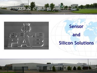
SlideShare a Scribd company logo
Sensor
                                                                                  and
                                                             Silicon Solutions


© Semefab (Scotland) Ltd.   Over 115 million semiconductor die shipped per year         www.semefab.com
Semefab Overview

 Custom Wafer Fabrication Solutions
                                                                   Global Fabrication Player
 Ship ~115 million die / year
                                                                   ~64% Export Bias
 Ship ~7.9 million MEMS die/year
                                                                   >35 Customers Worldwide
 Development Model
                                                                   £13.6M Capex Investment
 Volume Model
 Design Partnerships
                                                                    Fab 1: 2.0m – 3.0m
 Technology Transfers
                                                                    Fab 2: 0.8m
 Established 1986
 Private Ownership                                                 Fab 3: 0.8m


         © Semefab (Scotland) Ltd.     Over 115 million semiconductor die shipped per year   www.semefab.com
                                                                                                www.semefab.com
Manufacturing Operations

                                                  Diverse Process Portfolio
                                                   MEMS
Fab Operations                                     Si Gate CMOS & Opto CMOS
 Fab 1: 4” CMOS / Bipolar                         Metal Gate CMOS & PMOS
                                                   DI Complementary bipolar
 Fab 2: 4” & 6” MEMS
                                                   DI BiCMOS
 Fab 3: 6” CMOS / Bipolar
                                                   Linear Bipolar
 Wafer Test Operation                             DMOS RF MOSFET
 ISO9001, ISO14001                                Lateral FET
                                                   Low Noise N Channel JFET
 UL & ESA Approval
                                                   PiN Photo Diode
                                                   Power Bipolar
                                                   Fast Recovery Diode


      © Semefab (Scotland) Ltd.   Over 115 million semiconductor die shipped per year      www.semefab.com
                                                                                        www.semefab.com
Development Model
 Open Access Facility for Industry and Academia
     Technology Partnering
     Background & Foreground IP agreements
 Full Technology Cycle – Feasibility – Proof of Concept - Prototypes
 Commercialisation Focus
     Tangible Development Outcomes
     Funding Justification – Research, Venture Capital, Investor…
 In-house Design Simulation & External Partnerships
 Semefab Process Development & Process Engineering Integration
 Seamless Transition from Development to Volume
 In-house Test Operation for product development


      © Semefab (Scotland) Ltd.   Over 115 million semiconductor die shipped per year      www.semefab.com
                                                                                        www.semefab.com
Volume Model

 Fab 1: Fabrication capacity of 50,000 4” wafers per year
 Fab 2: Fabrication capacity of 25,000 4”/6” wafers per year
 Test floor supports wafer test & package test
    Electrical parametric testing
    Sensor functional testing i.e.low pressure etc.
    Actual device packaging is subcontracted

 Fab 3: Capacity 25,000 6” wafers volume per year
    Fab 3 build phase started November 2009
    Fab 3 scheduled operational date September 2010

 Semefab is your low risk, value-add fabrication partner


     © Semefab (Scotland) Ltd.     Over 115 million semiconductor die shipped per year      www.semefab.com
                                                                                         www.semefab.com
Project Management

 Semefab Project Owner is responsible for project induction
    Single point technical contact with customer

 Process Development Team induct process steps and document flow
    Development team manage seamless handover to process engineering

 Process Engineering formalise process run card & SPC control

 Production Control manage work-in-progress planning

 Customer service communicates delivery schedule to customer

 Open Access welcomes customer access to wafer fabs & test floor


       © Semefab (Scotland) Ltd.   Over 115 million semiconductor die shipped per year      www.semefab.com
                                                                                         www.semefab.com
End Use Portfolio

ASIC Portfolio:                       Foundry Portfolio:                                MEMS Portfolio:
 Optical Smoke Detector               Precision Op-Amps                                Pollution Control
 Light Sensing & Switching            JFET PIR Sensors                                 Automotive Engine Mgt
 Ionisation Smoke Detector  Secure Telecoms                                            Automotive Air Quality
 Garage Door Opener                   RF Base Stations & PMR                           Altimeters
 Automotive Wiper                     Audio Amplification                              Ear Thermometers
 Automotive Window Lift               Power Devices & Modules                          Medical Low Pressure
                                                                                        Sensing
 PSU Watchdog                         X-Ray Detection
                                                                                         Industrial Pressure
                                                                                        Sensing


          © Semefab (Scotland) Ltd.     Over 115 million semiconductor die shipped per year           www.semefab.com
                                                                                                   www.semefab.com
Fab1- CMOS1 Process Capability
 Projection Alignment to 2.5m
 Double Side Proximity Alignment to 5.0m
 Wet Etch - HF, BOE Al wet etch, Si Etch,
  Hot Orthophosphoric etch, Solvent Strip, Overlay etch
 Dry Etch – PolySi, SiO2, Nitride, Aluminium
 PECVD Low stress Nitride & Oxynitride, STS, ASM,Novellus-C1
 Furnace Stacks – LPCVD Nitride, Poly, Oxide
 Furnace Stacks – Thermal Oxidation, Diffusion, Boron & Phos Doping
 Ion Implant
 Sputter – AlSi, Al, Cu

        © Semefab (Scotland) Ltd.   Over 115 million semiconductor die shipped per year      www.semefab.com
                                                                                          www.semefab.com
Fab1 – CMOS1


                              425m2 Class 100


© Semefab (Scotland) Ltd.     Over 115 million semiconductor die shipped per year   www.semefab.com
Fab2 – MEMS2 Process Capability
 Oxidation / Low stress LPCVD Nitride                            PECVD Thin Films - SiO2, SiN, SiON
 Wet Etch - PDC, HF,                BOE, Al wet                  Wafer-Wafer & Wafer-Glass Bonding
 etch, Si Etch, Solvent Strip                                       Anodic, Eutectic, Fusion EVG 520IS
 KOH wet etch                                                    SVG8800 Coat/Develop track – bulk
 Acetone, NMP Lift-off                                            dispense
 Multi-Metal Sputter – Au, TiW, Al, AlSi,                        SVG8800 Coat/Develop track – syringe
 AlCu, Ti, Ni, NiCr, Al2O3, Constantan,                            dispense
  SiCr, Sn                                                        Polyimide – coat & bake
 Evaporation – Cr, Ni ,Pt, Au, Ti, Ta                            XeF2 dry etch release of polysilicon
 Dry Etch – 100 and 150mm LAM Oxide,                             Deep Reactive Ion Etch (Fab1 Annexe)
 Poly/Nitride                                                       STS Pegasus
 Double side aligner                                             Resist strip dry etch, Matrix 101
 Stepper- Nikon i10                                              Critical point drying CO2 / IPA


         © Semefab (Scotland) Ltd.         Over 115 million semiconductor die shipped per year      www.semefab.com
                                                                                                 www.semefab.com
Fab2 – MEMS2


                                                                             600 m2 Class 100

                                                                              Photo is Class 10


© Semefab (Scotland) Ltd.     Over 115 million semiconductor die shipped per year           www.semefab.com
3 Axis Accelerometer
   with integrated CMOS control circuitry on proof mass


© Semefab (Scotland) Ltd.   Over 115 million semiconductor die shipped per year   www.semefab.com
© Semefab (Scotland) Ltd.   Over 115 million semiconductor die shipped per year      www.semefab.com
                                                                                  www.semefab.com
Piezo-Resistive Pressure Sensor


© Semefab (Scotland) Ltd.   Over 115 million semiconductor die shipped per year   www.semefab.com
Fab3 – CMOS3
Fab 3 Scheduled Operational Date: September 2010


   © Semefab (Scotland) Ltd.    Over 115 million semiconductor die shipped per year   www.semefab.com
Fab3 – CMOS3

                   Spares and tooling


                                                    comp


                                                                    wip
                                                                                                                                                                                                                                           1,200 m2 Class 100
         ab
                                         Implanter
                                        Implanter
                                                                                                 insp
                                                                                                                                                                                                                                                Photo is Class 10
         ate                                         comp
         me                                                                                                         Changing area
                                                                    wip


          nt


                                        Implanter


                                                                                                                                                                                                                                                                                         wip    wip
                                                                                                                                                                                                                                                                                                                        QZ T
                                                                                                                                                                                                                                                                                                                         T SR                QZ R
                                                                                                                                                                                                                                                                                                                                              T DY

                                                                                                                                                                                             corridor


                                                                                                                                                                                                                                                                                                                                                      QZCN
                                                                                                                                                                                                                                                                                                                                                       T L
P0
E0
 6                    P0
                      E0
                       6
                                               KS


                                                                                                                                                                                   ts


                                                                                                                                                                                                                                                                                    WB


                                                                                                                                                                                                                                                                                                                                                      RD
                                                                                                                                                                                  s


                                                                                                                                                                                                                                      40
                                                                                                                                                                                                                                      9
                                                                                                                                                                                                                                                                                               insp                    insp
                                                                 insp


P0
E0
 5                   P0
                     E0
                      6                                                                                                                c5
                                                                                                                                       10
                                                                                                                                                                                                                                                                                               insp                    insp


                                                                                                                                                                                                                                                                                    RD


                                                                                                                                                                                                                                                                                                                                                      WB
                                                                                                                                                                                                                                                              D IE
                                                                                                                                                                                                                                                               R


                                                                                                                                                                                                                                                                                    m
                                                                                                                                                                                                                                                                                    s
                                                                                                                                                                                                                                          15


                                                                                                                                                                                                                                                                                    e
                                                                                                                                                                                                                                          0
                                                                                      L3
                                                                                      P


                                                                                                                                                                      insp


NneV
ik Ni
 ox
                                                            dv
                                                             e


                                                                                                                                                                                                               WB       RD   WB                                                                                                            TMX


                                                                                                                                                                                                                                     m
                                                                                                                                                                                                                                     es
                                                                                                        ceicl
                                                                                                        ha
                                                                                                         m                                                                                                                                                                                                                                Console


                                                                                                                                                                                                                                                 insp
               Photo area
                                                                                                                                                                                                                                                                                                                                                     Source


                                                                                                                                                                                                                                                                                                                                                                  Pumps
                                                                                                                                                                                                                                                                                                                                                     Cabinet
                                                                                                                                                        PVD & Metal                                                                                                                                                             STACK C
                                                                           ea u
                                                                          Cmlpsth
                                                                          h ic as r


                                                                                                                                            M 63
                                                                                                                                             rc 4


                                                                                                                                                                                                                                  Etch Area
                                                                                                                                                                                                   /t
                                                                                                                                                                                                   p


                                                                                                                                                                                                                                                          m
                                                                                                                                                                                                                                                          60
                                                                                                                                                                                                                                                         90
                                                                                                                                                                                                                                                         la
                                                                                                                Service area
                                                            ot
                                                            ca


                                                                                                                                                                                                                                                                     Service area
                                                                                                                                                                      load
     SE P R
      T PE


                                                                                                                                                                                                                                                 insp
                                                                                                                                                                                                                   WB   RD   WB

                                                                                                        ceicl
                                                                                                        ha
                                                                                                         m                                                                                                                                                                                                                      STACK B


                                                                                                                                                                                                                                                                                                                                                                  Pumps
                                                                                                                                                                                                                                                                                                                                                     Source
                                        insp


                                                                                                                                                                                                                                                                                                                                                     Cabinet
                                                            CD


                                                                                                                                                                                                                                                         m
                                                                                                                                                                                                                                                         40
                                                             &


                                                                                                                                                                                                                                                        42
                                                                                                                                                                                                                                                        la
                                                                                                                                                                                                                                                                                                                                            TMX
                                                                                                                                                                                                                                                                                                                                           Console
                                                                                                                                                                                                                                           91
                                                                                                                                                                                                                                            0

                                                                                                                                                                                                    Service area
                                                                            Tcprts
                                                                            r ka


                                                                                                                                        20
                                                                                                                                        39
                                                                             a


                                                                                                                                                                                                                                                                                                      Diffusion area
                                                                                                                                                                             WB


                                                                                                                                                                                                                                                                                                                                            TMX
                                                            CD
                                                             &


                                                                                                                                                                                                                                                                                                                                           Console
     SE P R
      T PE


                                                                                                                                                                                                                                                                                                                                                               Pumps
                                                                                                                                                                                                                                                                                                                                                     Source
                                                                                                                                                                             RD


                                                                                                                                                                                                                                                         m
                                                                                                                                                                                                                                                         50
                                                                                                                                                                                                                                                        42
                                                                                                                                                                                                                                                        la
                                                                                                                                                                                                                                                                                                                                                     Cabinet
                                                                                                                                                                                                                                           93
                                                                                                                                                                                                                                            0


                                                                                                                                                                                                                                                                                                                                STACK A
                                                                                       Ctc c p
                                                                                        ahu


                                                                                                                                                                                        /t
                                                                                                                                                                                        p
                                                                                                                                                    m
                                                                                                                                                    s


                                                                                                                               Stea
                                                                                                                               ptrpt
                                                                                                                                u rs
                                                                                                                                                    e


                                                    © Semefab (Scotland) Ltd.                                                                                                           Over 115 million semiconductor die shipped per year                                                                                     www.semefab.com
Fab3 – CMOS3 Process Capability
 Furnace Stack 1 Oxidation, Drive
 Furnace Stack 2 LPCVD BP-TEOS Nitride Standard and
  Low Stress, Poly (in situ phos doped)
 Furnace Stack 3 Boron Dep, Phos Dep, Alloy Oxidation
 Wet Etch – BOE, Metal etch, Solvent strip
 FSI Saturn/Mercury- PDC
 Nikon i11 Stepper
 Perkin Elmer Scanner
 SVG 8800 Resist spin / Develop
 LAM 4420 Oxide / Poly Etch
 LAM 4520 Nitride Etch
 LAM 9600 Metal Etch
 Varian 3290 Al, Al/Si, AlCu Sputter with pre-etch
 Varian 350DE x 2 Ion implant, B, P ,As


      © Semefab (Scotland) Ltd.   Over 115 million semiconductor die shipped per year   www.semefab.com
Fab3 – CMOS3 Process Capability
 Fab 3 Scheduled Operational Date: September 2010


© Semefab (Scotland) Ltd.   Over 115 million semiconductor die shipped per year   www.semefab.com
Test Operations Capability

 250m2 Class 100,000 Area with Class 100 Hoods
 Reedholm Instruments RI20/RI40 Parametric Tester (3)
 Tesec 8101TT - Discrete Device Tester (3kV/20A) (1)
 Exatron SOIC / DIP Handler (2)
 Multitest SOIC / DIP Handler –400C to +1250C (5)
 Electroglas 2001X Wafer Auto-prober (6)
 Wentworth 1050 Semi-auto Prober (high-voltage) (1)
 Thermostream


    © Semefab (Scotland) Ltd.   Over 115 million semiconductor die shipped per year      www.semefab.com
                                                                                      www.semefab.com
Probe & Test Layout


© Semefab (Scotland) Ltd.   Over 115 million semiconductor die shipped per year   www.semefab.com
Semefab’s Location…


                                                              Semefab (Scotland) Ltd.,
                                                                  Newark Road South,
              Semefab
                                                            Eastfield Industrial Estate,
                                                                 Glenrothes, Scotland,
                                                             United Kingdom, KY7 4NS
                                                         Telephone: +44 1592 630630
                                                                Fax: +44 1592 775265
                                                                    www.semefab.com


© Semefab (Scotland) Ltd.   Over 115 million semiconductor die shipped per year   www.semefab.com

More Related Content

Similar to Semefab Presentation

Atomic Layer Deposition solutions for SiC Power Electronics
Atomic Layer Deposition solutions for SiC Power ElectronicsAtomic Layer Deposition solutions for SiC Power Electronics
Atomic Layer Deposition solutions for SiC Power Electronics
Beneq
 
Commercializing RF SOI
Commercializing RF SOI Commercializing RF SOI
Commercializing RF SOI
RFSOI
 
OMMIC presentation on fabrication of MMIC integrated with MEMs RF
OMMIC presentation on fabrication of MMIC integrated with MEMs RFOMMIC presentation on fabrication of MMIC integrated with MEMs RF
OMMIC presentation on fabrication of MMIC integrated with MEMs RF
mick799252
 
Tft Product Presentation June 2009
Tft Product Presentation June 2009Tft Product Presentation June 2009
Tft Product Presentation June 2009
MikeWalsh1954
 
Allwin21 Product Brochures-Rapid Thermal Processors-2024.5.pdf
Allwin21 Product Brochures-Rapid Thermal Processors-2024.5.pdfAllwin21 Product Brochures-Rapid Thermal Processors-2024.5.pdf
Allwin21 Product Brochures-Rapid Thermal Processors-2024.5.pdf
Peter Chen
 
Qualcomm 60GHz WiGig/WiFi 802.11ad Chipset World’s First Smartphone Edition
Qualcomm 60GHz WiGig/WiFi 802.11ad Chipset World’s First Smartphone EditionQualcomm 60GHz WiGig/WiFi 802.11ad Chipset World’s First Smartphone Edition
Qualcomm 60GHz WiGig/WiFi 802.11ad Chipset World’s First Smartphone Edition
system_plus
 
Fcipt Overview
Fcipt OverviewFcipt Overview
Fcipt Overview
Mrs. Purvi Kikani Dave
 
Fcipt Overview
Fcipt OverviewFcipt Overview
Fcipt Overview
Mrs. Purvi Kikani Dave
 
Allwin21 Product Brochures-2024.5-email.pdf
Allwin21 Product Brochures-2024.5-email.pdfAllwin21 Product Brochures-2024.5-email.pdf
Allwin21 Product Brochures-2024.5-email.pdf
Peter Chen
 
MTP/MPO Cabling Solution - Gigalight Product Overview
MTP/MPO Cabling Solution - Gigalight Product OverviewMTP/MPO Cabling Solution - Gigalight Product Overview
MTP/MPO Cabling Solution - Gigalight Product Overview
Gigalight
 
Developing robust, 5V tolerant analog I/O libraries for CMOS processes & FinF...
Developing robust, 5V tolerant analog I/O libraries for CMOS processes & FinF...Developing robust, 5V tolerant analog I/O libraries for CMOS processes & FinF...
Developing robust, 5V tolerant analog I/O libraries for CMOS processes & FinF...
Sofics
 
USB Training - Silicon Labs -
USB Training - Silicon Labs -USB Training - Silicon Labs -
USB Training - Silicon Labs -
Emanuele Bonanni
 
HR-045-職場經驗分享
HR-045-職場經驗分享HR-045-職場經驗分享
HR-045-職場經驗分享handbook
 
Cmos scaling on resistive component 2012
Cmos scaling on resistive component 2012Cmos scaling on resistive component 2012
Cmos scaling on resistive component 2012
Sidewinder2011
 
Sample of product development
Sample of product developmentSample of product development
Sample of product development
Transit-Protect
 
NEGOCIOS DEL AMONIACO INNOVACION Y FUTURO EN CHILE
NEGOCIOS DEL AMONIACO INNOVACION Y FUTURO EN CHILENEGOCIOS DEL AMONIACO INNOVACION Y FUTURO EN CHILE
NEGOCIOS DEL AMONIACO INNOVACION Y FUTURO EN CHILE
zenzomaru
 
GaN-on-Si Substrate Technology and Market for LED and Power Electronics
GaN-on-Si Substrate Technology and Market for LED and Power ElectronicsGaN-on-Si Substrate Technology and Market for LED and Power Electronics
GaN-on-Si Substrate Technology and Market for LED and Power Electronics
Yole Developpement
 
PCB Fabrication Manufacturer Corporate Brochure
PCB Fabrication Manufacturer Corporate BrochurePCB Fabrication Manufacturer Corporate Brochure
PCB Fabrication Manufacturer Corporate Brochure
Domestic PCB Fabrication
 

Similar to Semefab Presentation (20)

CMOS SOI Technology
CMOS SOI TechnologyCMOS SOI Technology
CMOS SOI Technology
 
Atomic Layer Deposition solutions for SiC Power Electronics
Atomic Layer Deposition solutions for SiC Power ElectronicsAtomic Layer Deposition solutions for SiC Power Electronics
Atomic Layer Deposition solutions for SiC Power Electronics
 
Commercializing RF SOI
Commercializing RF SOI Commercializing RF SOI
Commercializing RF SOI
 
OMMIC presentation on fabrication of MMIC integrated with MEMs RF
OMMIC presentation on fabrication of MMIC integrated with MEMs RFOMMIC presentation on fabrication of MMIC integrated with MEMs RF
OMMIC presentation on fabrication of MMIC integrated with MEMs RF
 
Tft Product Presentation June 2009
Tft Product Presentation June 2009Tft Product Presentation June 2009
Tft Product Presentation June 2009
 
Allwin21 Product Brochures-Rapid Thermal Processors-2024.5.pdf
Allwin21 Product Brochures-Rapid Thermal Processors-2024.5.pdfAllwin21 Product Brochures-Rapid Thermal Processors-2024.5.pdf
Allwin21 Product Brochures-Rapid Thermal Processors-2024.5.pdf
 
Oerlikon Solar
Oerlikon SolarOerlikon Solar
Oerlikon Solar
 
Qualcomm 60GHz WiGig/WiFi 802.11ad Chipset World’s First Smartphone Edition
Qualcomm 60GHz WiGig/WiFi 802.11ad Chipset World’s First Smartphone EditionQualcomm 60GHz WiGig/WiFi 802.11ad Chipset World’s First Smartphone Edition
Qualcomm 60GHz WiGig/WiFi 802.11ad Chipset World’s First Smartphone Edition
 
Fcipt Overview
Fcipt OverviewFcipt Overview
Fcipt Overview
 
Fcipt Overview
Fcipt OverviewFcipt Overview
Fcipt Overview
 
Allwin21 Product Brochures-2024.5-email.pdf
Allwin21 Product Brochures-2024.5-email.pdfAllwin21 Product Brochures-2024.5-email.pdf
Allwin21 Product Brochures-2024.5-email.pdf
 
MTP/MPO Cabling Solution - Gigalight Product Overview
MTP/MPO Cabling Solution - Gigalight Product OverviewMTP/MPO Cabling Solution - Gigalight Product Overview
MTP/MPO Cabling Solution - Gigalight Product Overview
 
Developing robust, 5V tolerant analog I/O libraries for CMOS processes & FinF...
Developing robust, 5V tolerant analog I/O libraries for CMOS processes & FinF...Developing robust, 5V tolerant analog I/O libraries for CMOS processes & FinF...
Developing robust, 5V tolerant analog I/O libraries for CMOS processes & FinF...
 
USB Training - Silicon Labs -
USB Training - Silicon Labs -USB Training - Silicon Labs -
USB Training - Silicon Labs -
 
HR-045-職場經驗分享
HR-045-職場經驗分享HR-045-職場經驗分享
HR-045-職場經驗分享
 
Cmos scaling on resistive component 2012
Cmos scaling on resistive component 2012Cmos scaling on resistive component 2012
Cmos scaling on resistive component 2012
 
Sample of product development
Sample of product developmentSample of product development
Sample of product development
 
NEGOCIOS DEL AMONIACO INNOVACION Y FUTURO EN CHILE
NEGOCIOS DEL AMONIACO INNOVACION Y FUTURO EN CHILENEGOCIOS DEL AMONIACO INNOVACION Y FUTURO EN CHILE
NEGOCIOS DEL AMONIACO INNOVACION Y FUTURO EN CHILE
 
GaN-on-Si Substrate Technology and Market for LED and Power Electronics
GaN-on-Si Substrate Technology and Market for LED and Power ElectronicsGaN-on-Si Substrate Technology and Market for LED and Power Electronics
GaN-on-Si Substrate Technology and Market for LED and Power Electronics
 
PCB Fabrication Manufacturer Corporate Brochure
PCB Fabrication Manufacturer Corporate BrochurePCB Fabrication Manufacturer Corporate Brochure
PCB Fabrication Manufacturer Corporate Brochure
 

Semefab Presentation

  • 1. Sensor and Silicon Solutions © Semefab (Scotland) Ltd. Over 115 million semiconductor die shipped per year www.semefab.com
  • 2. Semefab Overview  Custom Wafer Fabrication Solutions  Global Fabrication Player  Ship ~115 million die / year  ~64% Export Bias  Ship ~7.9 million MEMS die/year  >35 Customers Worldwide  Development Model  £13.6M Capex Investment  Volume Model  Design Partnerships  Fab 1: 2.0m – 3.0m  Technology Transfers  Fab 2: 0.8m  Established 1986  Private Ownership  Fab 3: 0.8m © Semefab (Scotland) Ltd. Over 115 million semiconductor die shipped per year www.semefab.com www.semefab.com
  • 3. Manufacturing Operations Diverse Process Portfolio  MEMS Fab Operations  Si Gate CMOS & Opto CMOS  Fab 1: 4” CMOS / Bipolar  Metal Gate CMOS & PMOS  DI Complementary bipolar  Fab 2: 4” & 6” MEMS  DI BiCMOS  Fab 3: 6” CMOS / Bipolar  Linear Bipolar  Wafer Test Operation  DMOS RF MOSFET  ISO9001, ISO14001  Lateral FET  Low Noise N Channel JFET  UL & ESA Approval  PiN Photo Diode  Power Bipolar  Fast Recovery Diode © Semefab (Scotland) Ltd. Over 115 million semiconductor die shipped per year www.semefab.com www.semefab.com
  • 4. Development Model  Open Access Facility for Industry and Academia  Technology Partnering  Background & Foreground IP agreements  Full Technology Cycle – Feasibility – Proof of Concept - Prototypes  Commercialisation Focus  Tangible Development Outcomes  Funding Justification – Research, Venture Capital, Investor…  In-house Design Simulation & External Partnerships  Semefab Process Development & Process Engineering Integration  Seamless Transition from Development to Volume  In-house Test Operation for product development © Semefab (Scotland) Ltd. Over 115 million semiconductor die shipped per year www.semefab.com www.semefab.com
  • 5. Volume Model  Fab 1: Fabrication capacity of 50,000 4” wafers per year  Fab 2: Fabrication capacity of 25,000 4”/6” wafers per year  Test floor supports wafer test & package test  Electrical parametric testing  Sensor functional testing i.e.low pressure etc.  Actual device packaging is subcontracted  Fab 3: Capacity 25,000 6” wafers volume per year  Fab 3 build phase started November 2009  Fab 3 scheduled operational date September 2010  Semefab is your low risk, value-add fabrication partner © Semefab (Scotland) Ltd. Over 115 million semiconductor die shipped per year www.semefab.com www.semefab.com
  • 6. Project Management  Semefab Project Owner is responsible for project induction  Single point technical contact with customer  Process Development Team induct process steps and document flow  Development team manage seamless handover to process engineering  Process Engineering formalise process run card & SPC control  Production Control manage work-in-progress planning  Customer service communicates delivery schedule to customer  Open Access welcomes customer access to wafer fabs & test floor © Semefab (Scotland) Ltd. Over 115 million semiconductor die shipped per year www.semefab.com www.semefab.com
  • 7. End Use Portfolio ASIC Portfolio: Foundry Portfolio: MEMS Portfolio:  Optical Smoke Detector  Precision Op-Amps  Pollution Control  Light Sensing & Switching  JFET PIR Sensors  Automotive Engine Mgt  Ionisation Smoke Detector  Secure Telecoms  Automotive Air Quality  Garage Door Opener  RF Base Stations & PMR  Altimeters  Automotive Wiper  Audio Amplification  Ear Thermometers  Automotive Window Lift  Power Devices & Modules  Medical Low Pressure Sensing  PSU Watchdog  X-Ray Detection  Industrial Pressure Sensing © Semefab (Scotland) Ltd. Over 115 million semiconductor die shipped per year www.semefab.com www.semefab.com
  • 8. Fab1- CMOS1 Process Capability  Projection Alignment to 2.5m  Double Side Proximity Alignment to 5.0m  Wet Etch - HF, BOE Al wet etch, Si Etch, Hot Orthophosphoric etch, Solvent Strip, Overlay etch  Dry Etch – PolySi, SiO2, Nitride, Aluminium  PECVD Low stress Nitride & Oxynitride, STS, ASM,Novellus-C1  Furnace Stacks – LPCVD Nitride, Poly, Oxide  Furnace Stacks – Thermal Oxidation, Diffusion, Boron & Phos Doping  Ion Implant  Sputter – AlSi, Al, Cu © Semefab (Scotland) Ltd. Over 115 million semiconductor die shipped per year www.semefab.com www.semefab.com
  • 9. Fab1 – CMOS1 425m2 Class 100 © Semefab (Scotland) Ltd. Over 115 million semiconductor die shipped per year www.semefab.com
  • 10. Fab2 – MEMS2 Process Capability  Oxidation / Low stress LPCVD Nitride  PECVD Thin Films - SiO2, SiN, SiON  Wet Etch - PDC, HF, BOE, Al wet  Wafer-Wafer & Wafer-Glass Bonding etch, Si Etch, Solvent Strip Anodic, Eutectic, Fusion EVG 520IS  KOH wet etch  SVG8800 Coat/Develop track – bulk  Acetone, NMP Lift-off dispense  Multi-Metal Sputter – Au, TiW, Al, AlSi,  SVG8800 Coat/Develop track – syringe AlCu, Ti, Ni, NiCr, Al2O3, Constantan, dispense SiCr, Sn  Polyimide – coat & bake  Evaporation – Cr, Ni ,Pt, Au, Ti, Ta  XeF2 dry etch release of polysilicon  Dry Etch – 100 and 150mm LAM Oxide,  Deep Reactive Ion Etch (Fab1 Annexe) Poly/Nitride STS Pegasus  Double side aligner  Resist strip dry etch, Matrix 101  Stepper- Nikon i10  Critical point drying CO2 / IPA © Semefab (Scotland) Ltd. Over 115 million semiconductor die shipped per year www.semefab.com www.semefab.com
  • 11. Fab2 – MEMS2 600 m2 Class 100 Photo is Class 10 © Semefab (Scotland) Ltd. Over 115 million semiconductor die shipped per year www.semefab.com
  • 12. 3 Axis Accelerometer with integrated CMOS control circuitry on proof mass © Semefab (Scotland) Ltd. Over 115 million semiconductor die shipped per year www.semefab.com
  • 13. © Semefab (Scotland) Ltd. Over 115 million semiconductor die shipped per year www.semefab.com www.semefab.com
  • 14. Piezo-Resistive Pressure Sensor © Semefab (Scotland) Ltd. Over 115 million semiconductor die shipped per year www.semefab.com
  • 15. Fab3 – CMOS3 Fab 3 Scheduled Operational Date: September 2010 © Semefab (Scotland) Ltd. Over 115 million semiconductor die shipped per year www.semefab.com
  • 16. Fab3 – CMOS3 Spares and tooling comp wip 1,200 m2 Class 100 ab Implanter Implanter insp Photo is Class 10 ate comp me Changing area wip nt Implanter wip wip QZ T T SR QZ R T DY corridor QZCN T L P0 E0 6 P0 E0 6 KS ts WB RD s 40 9 insp insp insp P0 E0 5 P0 E0 6 c5 10 insp insp RD WB D IE R m s 15 e 0 L3 P insp NneV ik Ni ox dv e WB RD WB TMX m es ceicl ha m Console insp Photo area Source Pumps Cabinet PVD & Metal STACK C ea u Cmlpsth h ic as r M 63 rc 4 Etch Area /t p m 60 90 la Service area ot ca Service area load SE P R T PE insp WB RD WB ceicl ha m STACK B Pumps Source insp Cabinet CD m 40 & 42 la TMX Console 91 0 Service area Tcprts r ka 20 39 a Diffusion area WB TMX CD & Console SE P R T PE Pumps Source RD m 50 42 la Cabinet 93 0 STACK A Ctc c p ahu /t p m s Stea ptrpt u rs e © Semefab (Scotland) Ltd. Over 115 million semiconductor die shipped per year www.semefab.com
  • 17. Fab3 – CMOS3 Process Capability  Furnace Stack 1 Oxidation, Drive  Furnace Stack 2 LPCVD BP-TEOS Nitride Standard and Low Stress, Poly (in situ phos doped)  Furnace Stack 3 Boron Dep, Phos Dep, Alloy Oxidation  Wet Etch – BOE, Metal etch, Solvent strip  FSI Saturn/Mercury- PDC  Nikon i11 Stepper  Perkin Elmer Scanner  SVG 8800 Resist spin / Develop  LAM 4420 Oxide / Poly Etch  LAM 4520 Nitride Etch  LAM 9600 Metal Etch  Varian 3290 Al, Al/Si, AlCu Sputter with pre-etch  Varian 350DE x 2 Ion implant, B, P ,As © Semefab (Scotland) Ltd. Over 115 million semiconductor die shipped per year www.semefab.com
  • 18. Fab3 – CMOS3 Process Capability Fab 3 Scheduled Operational Date: September 2010 © Semefab (Scotland) Ltd. Over 115 million semiconductor die shipped per year www.semefab.com
  • 19. Test Operations Capability  250m2 Class 100,000 Area with Class 100 Hoods  Reedholm Instruments RI20/RI40 Parametric Tester (3)  Tesec 8101TT - Discrete Device Tester (3kV/20A) (1)  Exatron SOIC / DIP Handler (2)  Multitest SOIC / DIP Handler –400C to +1250C (5)  Electroglas 2001X Wafer Auto-prober (6)  Wentworth 1050 Semi-auto Prober (high-voltage) (1)  Thermostream © Semefab (Scotland) Ltd. Over 115 million semiconductor die shipped per year www.semefab.com www.semefab.com
  • 20. Probe & Test Layout © Semefab (Scotland) Ltd. Over 115 million semiconductor die shipped per year www.semefab.com
  • 21. Semefab’s Location… Semefab (Scotland) Ltd., Newark Road South, Semefab Eastfield Industrial Estate, Glenrothes, Scotland, United Kingdom, KY7 4NS Telephone: +44 1592 630630 Fax: +44 1592 775265 www.semefab.com © Semefab (Scotland) Ltd. Over 115 million semiconductor die shipped per year www.semefab.com