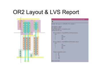
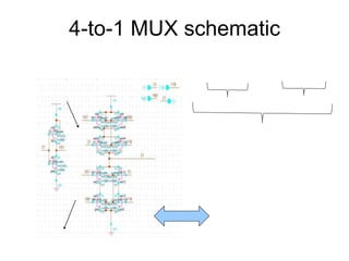
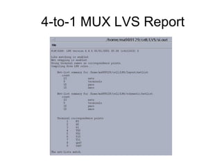
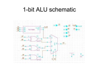
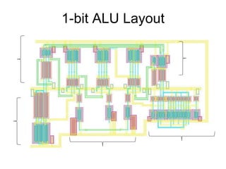
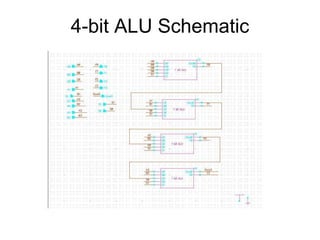
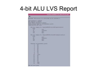
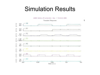
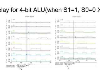
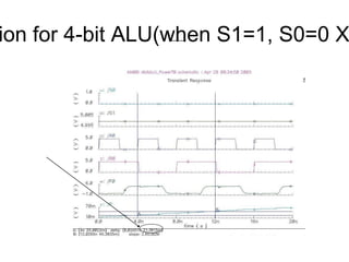
This document describes the design and simulation of a 4-bit arithmetic logic unit (ALU) circuit. It includes block diagrams and schematics of the logic gates, full adder, 4-to-1 multiplexer, 1-bit ALU, and 4-bit ALU. Simulation results demonstrate the circuit's functionality when performing operations on different input patterns, and propagation delays are reported for each component.


![20230809133941_[11] 27 Datapath Introduction_1 NEW.pptx](https://cdn.slidesharecdn.com/ss_thumbnails/202308091339411127datapathintroduction1new-251108061328-e0605b9a-thumbnail.jpg?width=640&height=640&fit=bounds)


