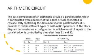
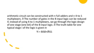
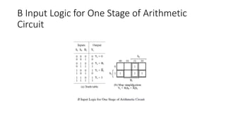
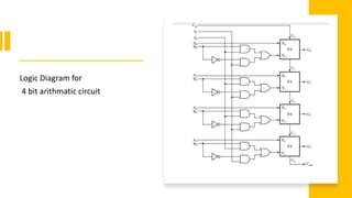
KSR College of engineering
Name :S.Hari Prasanth
Reg no :7448959023
Sub name :Digital principal and
computer design
Sub code :20EE231
COMPUTER DESIGN
BASICS :
• COMPUTER DESIGN BASICS The specification for a
computer consists of to a programmer at the lowest
level, its instruction set architecture (ISA). From the
ISA, a high-level description of the hardware to
implement the computer, called the computer
architecture, is formulated. This architecture, for a
simple computer, is typically divided into a datapath
and a control. The datapath is defined by three basic
components: 1. a set of registers, 2. the
microoperations performed on data stored in the
registers, and 3. the control interface.
DATAPATHS or
PROCESSOR
ORGANIZATION
Sometimes processor organization is also
called DATAPATH To perform its micro
operations directly, computer systems often
employ a number of storage registers in
conjunction with a shared operation unit
called an arithmetic/logic unit, ALU. To
perform a micro operation, the contents of
specified source registers are applied to the
inputs of the shared ALU. The ALU
performs an operation, and the result of this
operation is transferred to a destination
register
The data path and the control unit are
the two parts of the processor, or CPU,
of a computer. In addition to the
registers, the datapath contains the
digital logic that implements the various
microoperations. This digital logic
consists of buses,multiplexers, decoders,
and processing circuits. When a large
number of registers is included in a
datapath, the registers are most
conveniently connected through one or
more buses. Registers in a datapath
interact by the direct transfer of data, as
well as in the performance of the various
types of microoperations
CONTROL
UNIT
• For example, to perform the microoperation
R1 <-R2+R3
the control unit must provide binary selection values to the
following sets of control inputs:
1. A select, to place the contents of R2 onto A data and, hence,
Bus A. 2. B select, to place the contents of R3 onto the 0 input of
MUX B; and MB select, to put the 0 input of MUX B onto Bus B.
3. G select, to provide the arithmetic operation A plus B.
4. MF select, to place the ALU output on the MUX F output.
5. MD select, to place the MUX F output onto Bus D.
6. Destination select, to select R1 as the destination of the data
on Bus D.
7. Load enable, to enable a register—in this case, R1—to be
loaded.
• The sets of values must be generated and must become available on the corresponding
control lines early in the clock cycle. The binary data from the two source registers
must propagate through the multiplexers and the ALU and on into the inputs of the
destination register, all during the remainder of the same clock cycle. Then, when the
next positive clock edge arrives, the binary data on Bus D is loaded into the destination
register. To achieve fast operation, the ALU and shifter are constructed with
combinational logic having a limited number of levels
ARITHMETIC/LOGIC UNIT
The ALU is a combinational circuit that performs a
set of basic arithmetic and logic microoperations.
It has a number of selection lines used to
determine the operation to be performed.The
selection lines are decoded within the ALU, so that
k selection lines can specify up to 2k distinct
operations. Figure shows the symbol for a typical
n-bit ALU. The n data inputs from A are combined
with the n inputs from B to generate the result of
an operation at the G outputs. The mode-select
input S2 distinguishes between arithmetic and logic
operations. The two Operation select inputs S1
and S0 and the Carry input Cin specify the eight
arithmetic operations with S2 at 0. Operand select
input S0 and Cin specify the four logic operations
with S2 at 1.
ARITHMETIC CIRCUIT
The basic component of an arithmetic circuit is a parallel adder, which
is constructed with a number of full-adder circuits connected in
cascade. By controlling the data inputs to the parallel adder, it is
possible to obtain different types of arithmetic operations. The block
diagram demonstrates a configuration in which one set of inputs to the
parallel adder is controlled by the select lines S1 and S0.
arithmetic circuit can be constructed with n full adders and n 4-to-1
multiplexers. The number of gates in the B input logic can be reduced
if, instead of using 4-to-1 multiplexers, we go through the logic design
of one stage (one bit) of the B input logic. The truth table for one
typical stage i of the logic is given in
Yi = BiS0+𝐵̅iS1
B Input Logic for One Stage of Arithmetic
Circuit
Logic Diagram for
4 bit arithmatic circuit

Presentation 4.pptx

  • 1.
    KSR College ofengineering Name :S.Hari Prasanth Reg no :7448959023 Sub name :Digital principal and computer design Sub code :20EE231
  • 2.
    COMPUTER DESIGN BASICS : •COMPUTER DESIGN BASICS The specification for a computer consists of to a programmer at the lowest level, its instruction set architecture (ISA). From the ISA, a high-level description of the hardware to implement the computer, called the computer architecture, is formulated. This architecture, for a simple computer, is typically divided into a datapath and a control. The datapath is defined by three basic components: 1. a set of registers, 2. the microoperations performed on data stored in the registers, and 3. the control interface.
  • 3.
    DATAPATHS or PROCESSOR ORGANIZATION Sometimes processororganization is also called DATAPATH To perform its micro operations directly, computer systems often employ a number of storage registers in conjunction with a shared operation unit called an arithmetic/logic unit, ALU. To perform a micro operation, the contents of specified source registers are applied to the inputs of the shared ALU. The ALU performs an operation, and the result of this operation is transferred to a destination register
  • 4.
    The data pathand the control unit are the two parts of the processor, or CPU, of a computer. In addition to the registers, the datapath contains the digital logic that implements the various microoperations. This digital logic consists of buses,multiplexers, decoders, and processing circuits. When a large number of registers is included in a datapath, the registers are most conveniently connected through one or more buses. Registers in a datapath interact by the direct transfer of data, as well as in the performance of the various types of microoperations
  • 5.
    CONTROL UNIT • For example,to perform the microoperation R1 <-R2+R3 the control unit must provide binary selection values to the following sets of control inputs: 1. A select, to place the contents of R2 onto A data and, hence, Bus A. 2. B select, to place the contents of R3 onto the 0 input of MUX B; and MB select, to put the 0 input of MUX B onto Bus B. 3. G select, to provide the arithmetic operation A plus B. 4. MF select, to place the ALU output on the MUX F output. 5. MD select, to place the MUX F output onto Bus D. 6. Destination select, to select R1 as the destination of the data on Bus D. 7. Load enable, to enable a register—in this case, R1—to be loaded.
  • 6.
    • The setsof values must be generated and must become available on the corresponding control lines early in the clock cycle. The binary data from the two source registers must propagate through the multiplexers and the ALU and on into the inputs of the destination register, all during the remainder of the same clock cycle. Then, when the next positive clock edge arrives, the binary data on Bus D is loaded into the destination register. To achieve fast operation, the ALU and shifter are constructed with combinational logic having a limited number of levels
  • 7.
    ARITHMETIC/LOGIC UNIT The ALUis a combinational circuit that performs a set of basic arithmetic and logic microoperations. It has a number of selection lines used to determine the operation to be performed.The selection lines are decoded within the ALU, so that k selection lines can specify up to 2k distinct operations. Figure shows the symbol for a typical n-bit ALU. The n data inputs from A are combined with the n inputs from B to generate the result of an operation at the G outputs. The mode-select input S2 distinguishes between arithmetic and logic operations. The two Operation select inputs S1 and S0 and the Carry input Cin specify the eight arithmetic operations with S2 at 0. Operand select input S0 and Cin specify the four logic operations with S2 at 1.
  • 8.
    ARITHMETIC CIRCUIT The basiccomponent of an arithmetic circuit is a parallel adder, which is constructed with a number of full-adder circuits connected in cascade. By controlling the data inputs to the parallel adder, it is possible to obtain different types of arithmetic operations. The block diagram demonstrates a configuration in which one set of inputs to the parallel adder is controlled by the select lines S1 and S0.
  • 9.
    arithmetic circuit canbe constructed with n full adders and n 4-to-1 multiplexers. The number of gates in the B input logic can be reduced if, instead of using 4-to-1 multiplexers, we go through the logic design of one stage (one bit) of the B input logic. The truth table for one typical stage i of the logic is given in Yi = BiS0+𝐵̅iS1
  • 10.
    B Input Logicfor One Stage of Arithmetic Circuit
  • 11.
    Logic Diagram for 4bit arithmatic circuit