Combinational Logic Circuits Guide
•
1 like•99 views

2.1 Combinational Circuits § Characteristics § Logic circuit design § Block diagram, features & Applications of § adders,subtractors and comparators § multiplexers, demultiplexers § encoders, decoders and code converters (7 segment) 2.2 Sequential Circuits § Characteristics § Types § Asynchronous § Synchronous (clocked, un clocked) § Flip flops o Types, circuit analysis and truth table § Applications of sequential circuits o Shift registers (types and

Recommended
More Related Content
What's hot
What's hot (20)
Similar to Combinational Logic Circuits Guide
Similar to Combinational Logic Circuits Guide (20)
More from THANMAY JS
More from THANMAY JS (20)
Recently uploaded
Recently uploaded (20)
Combinational Logic Circuits Guide
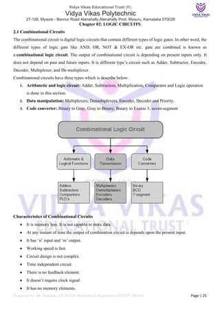
- 1. Vidya Vikas Educational Trust (R), Vidya Vikas Polytechnic 27-128, Mysore - Bannur Road Alanahally,Alanahally Post, Mysuru, Karnataka 570028 Prepared by: Mr Thanmay J.S, H.O.D Mechanical Engineering VVETP, Mysore Page | 25 Chapter 02: LOGIC CIRCUITS 2.1 Combinational Circuits The combinational circuit is digital logic circuits that contain different types of logic gates. In other word, the different types of logic gate like AND, OR, NOT & EX-OR etc. gate are combined is known as a combinational logic circuit. The output of combinational circuit is depending on present inputs only. It does not depend on past and future inputs. It is different type’s circuit such as Adder, Subtractor, Encoder, Decoder, Multiplexer, and De-multiplexer. Combinational circuits have three types which is describe below: 1. Arithmetic and logic circuit: Adder, Subtraction, Multiplication, Comparator and Logic operation is done in this section. 2. Data manipulation: Multiplexers, Demultiplexers, Encoder, Decoder and Priority. 3. Code converter: Binary to Gray, Gray to Binary, Binary to Excess 3, seven-segment Characteristics of Combinational Circuits • It is memory less. It is not capable to store data. • At any instant of time the output of combination circuit is depends upon the present input. • It has ‘n’ input and ‘m’ output. • Working speed is fast. • Circuit design is not complex. • Time independent circuit. • There is no feedback element. • It doesn’t require clock signal. • It has no memory elements.
- 2. Vidya Vikas Educational Trust (R), Vidya Vikas Polytechnic 27-128, Mysore - Bannur Road Alanahally,Alanahally Post, Mysuru, Karnataka 570028 Prepared by: Mr Thanmay J.S, H.O.D Mechanical Engineering VVETP, Mysore Page | 26 Logic circuit design The three main ways of specifying the function of a combinational logic circuit are: 1. Boolean Algebra – This forms the algebraic expression showing the operation of the logic circuit for each input variable either True or False that results in a logic “1” output. 2. Truth Table – A truth table defines the function of a logic gate by providing a concise list that shows all the output states in tabular form for each possible combination of input variable that the gate could encounter. 3. Logic Diagram – This is a graphical representation of a logic circuit that shows the wiring and connections of each individual logic gate, represented by a specific All three of these logic circuit representations are shown below logic design, basic organization of the circuitry of a digital computer. All digital computers are based on a two-valued logic system—1/0, on/off, yes/no (see binary code). Computers perform calculations using components called logic gates (or logic circuits), which are made up of integrated circuits that receive an input signal, process it, and change it into an output signal.
- 3. Vidya Vikas Educational Trust (R), Vidya Vikas Polytechnic 27-128, Mysore - Bannur Road Alanahally,Alanahally Post, Mysuru, Karnataka 570028 Prepared by: Mr Thanmay J.S, H.O.D Mechanical Engineering VVETP, Mysore Page | 27 Applications of Logic Circuits in adders There are two types Half and Full Adder Logic Circuits Half Adder: A combinational logic circuit which is designed to add two binary digits is called as a half adder. The half adder provides the output along with a carry value (if any). The half adder circuit is designed by connecting an EX-OR gate and one AND gate. It has two input terminals and two output terminals for sum and carry. The block diagram and circuit diagram of a half adder are shown in Figure-1. In the case of a half adder, the output of the EX-OR gate is the sum of two bits and the output of the AND gate is the carry. Although, the carry obtained in one addition will not be forwarded in the next addition because of this it is known as half adder. Full Adder: A combinational logic circuit that can add two binary digits (bits) and a carry bit, and produces a sum bit and a carry bit as output is known as a full-adder. In other words, a combinational circuit which is designed to add three binary digits and produces two outputs (sum and carry) is known as a full adder. Thus, a full adder circuit adds three binary digits, where two are the inputs and one is the carry forwarded from the previous addition. The block diagram and circuit diagram of the full adder are shown in Figure below. Hence, from the truth table, it is clear that the sum output of the full adder is equal to 1 when only 1 input is equal to 1 or when all the inputs are equal to 1. While the carry output has a carry of 1 if two or three inputs are equal to 1.
- 4. Vidya Vikas Educational Trust (R), Vidya Vikas Polytechnic 27-128, Mysore - Bannur Road Alanahally,Alanahally Post, Mysuru, Karnataka 570028 Prepared by: Mr Thanmay J.S, H.O.D Mechanical Engineering VVETP, Mysore Page | 28 Applications of Logic Circuits in subtractors Similar to adders, subtractors are also of two types −Half Subtractor and Full Subtractor Half Subtractor: A half-subtractor is a combinational logic circuit that have two inputs and two outputs (i.e., difference and borrow). The half subtractor produces the difference between the two binary bits at the input and also produces a borrow output (if any). In the subtraction (A-B), A is called as Minuend bit and B is called as Subtrahend bit. The block diagram and logic circuit diagram of the half subtractor is shown in Figure below. Hence, from the logic circuit diagram, it is clear that a half subtractor can be realized using an XOR gate together with a NOT gate and an AND gate. Full Subtractor: A full-subtractor is a combinational circuit that has three inputs A, B, bin and two outputs d and b. Where, A is the minuend, B is subtrahend, bin is borrow produced by the previous stage, d is the difference output and b is the borrow output. Since, the half subtractor can only be used to find the difference of LSBs (Least Significant Bits) of two binary numbers. Thus, if there is any borrow during the subtraction of the LSBs, it will affect the subtraction of the next bits of numbers. To overcome this problem of the half subtractor, a full subtractor is realized. The block diagram and circuit diagram of a full-subtractor is shown in Figure below.
- 5. Vidya Vikas Educational Trust (R), Vidya Vikas Polytechnic 27-128, Mysore - Bannur Road Alanahally,Alanahally Post, Mysuru, Karnataka 570028 Prepared by: Mr Thanmay J.S, H.O.D Mechanical Engineering VVETP, Mysore Page | 29 Applications of Logic Circuits in comparators • Multiplexers It is a combinational circuit which have many data inputs and single output depending on control or select inputs. For N input lines, log n (base2) selection lines, or we can say that for 2n input lines, n selection lines are required. Multiplexers are also known as “Data n selector, parallel to serial convertor, many to one circuit, universal logic circuit”. Multiplexers are mainly used to increase amount of the data that can be sent over the network within certain amount of time and bandwidth. Now the implementation of 4:1 Multiplexer using truth table and gates. Multiplexer can act as universal combinational circuit. All the standard logic gates can be implemented with multiplexers.
- 6. Vidya Vikas Educational Trust (R), Vidya Vikas Polytechnic 27-128, Mysore - Bannur Road Alanahally,Alanahally Post, Mysuru, Karnataka 570028 Prepared by: Mr Thanmay J.S, H.O.D Mechanical Engineering VVETP, Mysore Page | 30 • Demultiplexers A De-multiplexer is a combinational circuit that has only 1 input line and 2N output lines. Simply, the multiplexer is a single-input and multi-output combinational circuit. The information is received from the single input lines and directed to the output line. On the basis of the values of the selection lines, the input will be connected to one of these outputs. De-multiplexer is opposite to the multiplexer. Unlike encoder and decoder, there are n selection lines and 2n outputs. So, there is a total of 2n possible combinations of inputs. De-multiplexer is also treated as De-mux. There are various types of De-multiplexer which are as follows: • 1×2 De-multiplexer • 1×4 De-multiplexer • 1×8 De-multiplexer Example: 1×4 De-multiplexer: In 1 to 4 De-multiplexers, there are total of four outputs, i.e., Y0, Y1, Y2, and Y3, 2 selection lines, i.e., S0 and S1 and single input, i.e., A. On the basis of the combination of inputs which are present at the selection lines S0 and S1, the input be connected to one of the outputs. The block diagram and the truth table of the 1×4 multiplexer is given below. Block Diagram: The logical expression of the term Y is as follows: Y0=S1'.S0'.A y1=S1'.S0.A y2=S1.S0'.A y3=S1.S0.A Logical circuit of the above expressions is given below:
- 7. Vidya Vikas Educational Trust (R), Vidya Vikas Polytechnic 27-128, Mysore - Bannur Road Alanahally,Alanahally Post, Mysuru, Karnataka 570028 Prepared by: Mr Thanmay J.S, H.O.D Mechanical Engineering VVETP, Mysore Page | 31 • Encoders The combinational circuits that change the binary information into N output lines are known as Encoders. The binary information is passed in the form of 2N input lines. The output lines define the N-bit code for the binary information. In simple words, the Encoder performs the reverse operation of the Decoder. At a time, only one input line is activated for simplicity. The produced N-bit output code is equivalent to the binary information. There are various types of encoders which are as follows: • 4-to-2-line Encoder • 8-to-3-line Encoder • Decimal to BCD Encoder • Priority Encoder Example: 4-to-2-line Encoder: In 4-to-2-line encoder, there are total of four inputs, i.e., Y0, Y1, Y2, and Y3, and two outputs, i.e., A0 and A1. In 4-input lines, one input-line is set to true at a time to get the respective binary code in the output side. Below are the block diagram and the truth table of the 4-to-2-line encoder. Block Diagram Truth Table The logical expression of the term A0 and A1 is as follows: A1=Y3+Y2 A0=Y3+Y1 Logical circuit of the above expressions is given as follows:
- 8. Vidya Vikas Educational Trust (R), Vidya Vikas Polytechnic 27-128, Mysore - Bannur Road Alanahally,Alanahally Post, Mysuru, Karnataka 570028 Prepared by: Mr Thanmay J.S, H.O.D Mechanical Engineering VVETP, Mysore Page | 32 • decoders The combinational circuit that changes the binary information into 2N output lines is known as Decoders. The binary information is passed in the form of N input lines. The output lines define the 2N -bit code for the binary information. In simple words, the Decoder performs the reverse operation of the Encoder. At a time, only one input line is activated for simplicity. The produced 2N -bit output code is equivalent to the binary information. There are various types of decoders which are as follows: • 2-to-4-line decoder • 3-to-8-line decoder • 4-to-16-line Decoder Example: 2-to-4-line decoder In the 2-to-4-line decoder, there is a total of three inputs, i.e., A0, and A1 and E and four outputs, i.e., Y0, Y1, Y2, and Y3. For each combination of inputs, when the enable 'E' is set to 1, one of these four outputs will be 1. The block diagram and the truth table of the 2-to-4-line decoder are given below. Block Diagram: The logical expression of the term Y0, Y0, Y2, and Y3 is as follows: Y3=E.A1.A0 Y2=E.A1.A0' Y1=E.A1'.A0 Y0=E.A1'.A0' Logical circuit of the above expressions is given below:
- 9. Vidya Vikas Educational Trust (R), Vidya Vikas Polytechnic 27-128, Mysore - Bannur Road Alanahally,Alanahally Post, Mysuru, Karnataka 570028 Prepared by: Mr Thanmay J.S, H.O.D Mechanical Engineering VVETP, Mysore Page | 33 • code converters (7 segment) In Binary Coded Decimal (BCD) encoding scheme each of the decimal numbers (0-9) is represented by its equivalent binary pattern (which is generally of 4-bits). Whereas, seven segment display is an electronic device which consists of seven Light Emitting Diodes (LEDs) arranged in some definite pattern (common cathode or common anode type), which is used to display Hexadecimal numerals (in this case decimal numbers, as input is BCD i.e., 0-9). Two types of seven segment LED display: 1. Common Cathode Type: In this type of display all cathodes of the seven LEDs are connected together to the ground or -Vcc (hence, common cathode) and LED displays digits when some ‘HIGH’ signal is supplied to the individual anodes. 2. Common Anode Type: In this type of display all the anodes of the seven LEDs are connected to battery or +Vcc and LED displays digits when some ‘LOW’ signal is supplied to the individual cathodes. But, seven segment display does not work by directly supplying voltage to different segments of LEDs. First, our decimal number is changed to its BCD equivalent signal then BCD to seven segment decoder converts those signals to the form which is fed to seven segment display. This BCD to seven segment decoders has four input lines (A, B, C and D) and 7 output lines (a, b, c, d, e, f and g), this output is given to seven segment LED display which displays the decimal number depending upon inputs. Note: • For Common Anode type seven segment LED display, we only have to interchange all ‘0s’ and ‘1s’ in the output side i.e., (for a, b, c, d, e, f, and g replace all ‘1’ by ‘0’ and vice versa) and solve using K-map. • Output for first combination of inputs (A, B, C and D) in Truth Table corresponds to ‘0’ and last combination corresponds to ‘9’. Similarly rest corresponds from 2 to 8 from top to bottom. • BCD numbers only range from 0 to 9, thus rest inputs from 10-F are invalid inputs.
- 10. Vidya Vikas Educational Trust (R), Vidya Vikas Polytechnic 27-128, Mysore - Bannur Road Alanahally,Alanahally Post, Mysuru, Karnataka 570028 Prepared by: Mr Thanmay J.S, H.O.D Mechanical Engineering VVETP, Mysore Page | 34 2.2 Sequential Circuits The combinational circuits have set of outputs, which depends only on the present combination of inputs. Below is the block diagram of the synchronous logic circuit. The sequential circuit is a special type of circuit that has a series of inputs and outputs. The outputs of the sequential circuits depend on both the combination of present inputs and previous outputs. The previous output is treated as the present state. So, the sequential circuit contains the combinational circuit and its memory storage elements. A sequential circuit doesn't need to always contain a combinational circuit. So, the sequential circuit can contain only the memory element. Sequential circuits are digital circuits that store and use the previous state information to determine their next state. Unlike combinational circuits, which only depend on the current input values to produce outputs, sequential circuits depend on both the current inputs and the previous state stored in memory elements. Difference between the combinational circuits and sequential circuits are given below: Combinational Circuits Sequential Circuits 1) The outputs of the combinational circuit depend only on the present inputs. The outputs of the sequential circuits depend on both present inputs and present state (previous output). 2) The feedback path is not present in the combinational circuit. The feedback path is present in the sequential circuits. 3) In combinational circuits, memory elements are not required. In the sequential circuit, memory elements play an important role and require. 4) The clock signal is not required for combinational circuits. The clock signal is required for sequential circuits. 5) The combinational circuit is simple to design. It is not simple to design a sequential circuit. 0sPlay Video • Advantages of Sequential Circuits 1. Memory: Sequential circuits have the ability to store binary values, which makes them ideal for applications that require memory elements, such as timers and counters. 2. Timing: Sequential circuits are commonly used to implement timing and synchronization in digital systems, making them essential for real-time control applications. 3. State machine implementation: Sequential circuits can be used to implement state machines, which are useful for controlling complex digital systems and ensuring that they operate as intended. 4. Error detection: Sequential circuits can be designed to detect errors in digital systems and respond accordingly, improving the reliability of digital systems.
- 11. Vidya Vikas Educational Trust (R), Vidya Vikas Polytechnic 27-128, Mysore - Bannur Road Alanahally,Alanahally Post, Mysuru, Karnataka 570028 Prepared by: Mr Thanmay J.S, H.O.D Mechanical Engineering VVETP, Mysore Page | 35 • Types of sequential circuits There are two types of sequential circuits: a) Asynchronous sequential circuit b) synchronous sequential circuit Type 1: Asynchronous sequential circuit: These circuits do not use a clock signal but uses the pulses of the inputs. These circuits are faster than synchronous sequential circuits because there is clock pulse and change their state immediately when there is a change in the input signal. We use asynchronous sequential circuits when speed of operation is important and independent of internal clock pulse. But these circuits are more difficult to design and their output is uncertain. Type2: Synchronous sequential circuit: These circuits use clock signal and level inputs (or pulsed) (with restrictions on pulse width and circuit propagation). The output pulse is the same duration as the clock pulse for the clocked sequential circuits. Since they wait for the next clock pulse to arrive to perform the next operation, so these circuits are bit slower compared to asynchronous. Level output changes state at the start of an input pulse and remains in that until the next input or clock pulse. We use synchronous sequential circuit in synchronous counters, flip flops, and to design Counters, Registers, RAM, MOORE/MEALY Machine and other state retaining machines. • Flip flops Flip-flop is a circuit that maintains a state until directed by input to change the state. A basic flip-flop can be constructed using four-NAND or four-NOR gates. Types of flip-flops: 1. SR Flip Flop 2. JK Flip Flop 3. D Flip Flop 4. T Flip Flop Logic diagrams and truth tables of the different types of flip-flops are as follows:
- 12. Vidya Vikas Educational Trust (R), Vidya Vikas Polytechnic 27-128, Mysore - Bannur Road Alanahally,Alanahally Post, Mysuru, Karnataka 570028 Prepared by: Mr Thanmay J.S, H.O.D Mechanical Engineering VVETP, Mysore Page | 36 S-R Flip Flop: Characteristics Equation for SR Flip Flop: QN+1 = QNR’ + SR’ J-K Flip Flop: Characteristics Equation for JK Flip Flop: QN+1 = JQ’N + K’QN D Flip Flop: Characteristics Equation for D Flip Flop: QN+1 = D
- 13. Vidya Vikas Educational Trust (R), Vidya Vikas Polytechnic 27-128, Mysore - Bannur Road Alanahally,Alanahally Post, Mysuru, Karnataka 570028 Prepared by: Mr Thanmay J.S, H.O.D Mechanical Engineering VVETP, Mysore Page | 37 T Flip Flop: Characteristics Equation for T Flip Flop: QN+1 = Q’NT + QNT’ = QN XOR T • Applications of sequential circuits i. Shift registers (types and application): A group of flip flops which is used to store multiple bits of data and the data is moved from one flip flop to another is known as Shift Register. The bits stored in registers shifted when the clock pulse is applied within and inside or outside the registers. To form an n-bit shift register, we have to connect n number of flip flops. So, the number of bits of the binary number is directly proportional to the number of flip flops. The flip flops are connected in such a way that the first flip flop's output becomes the input of the other flip flop. A Shift Register can shift the bits either to the left or to the right. A Shift Register, which shifts the bit to the left, is known as "Shift left register", and it shifts the bit to the right, known as "Right left register". The shift register is classified into the following types: a) Serial In Serial Out b) Serial In Parallel Out c) Parallel In Serial Out d) Parallel In Parallel Out e) Bi-directional Shift Register f) Universal Shift Register Applications of Shift Registers • The shift registers are used for temporary data storage. • The shift registers are also used for data transfer and data manipulation. • The serial-in serial-out and parallel-in parallel-out shift registers are used to produce time delay to digital circuits. • The serial-in parallel-out shift register is used to convert serial data into parallel data thus they are used in communication lines where demultiplexing of a data line into several parallel lines is required. • A Parallel in Serial out shift register is used to convert parallel data to serial data.
- 14. Vidya Vikas Educational Trust (R), Vidya Vikas Polytechnic 27-128, Mysore - Bannur Road Alanahally,Alanahally Post, Mysuru, Karnataka 570028 Prepared by: Mr Thanmay J.S, H.O.D Mechanical Engineering VVETP, Mysore Page | 38 ii. Counters (classification and application) A special type of sequential circuit used to count the pulse is known as a counter, or a collection of flip flops where the clock signal is applied is known as counters. The counter is one of the widest applications of the flip flop. Based on the clock pulse, the output of the counter contains a predefined state. The number of the pulse can be counted using the output of the counter. There are the following types of counters: o Asynchronous Counters o Synchronous Counters 1) Asynchronous or ripple counters The Asynchronous counter is also known as the ripple counter. Below is a diagram of the 2-bit Asynchronous counter in which we used two T flip-flops. Apart from the T flip flop, we can also use the JK flip flop by setting both of the inputs to 1 permanently. The external clock pass to the clock input of the first flip flop, i.e., FF-A and its output, i.e., is passed to clock input of the next flip flop, i.e., FF-B. Block Diagram Signal Diagram
- 15. Vidya Vikas Educational Trust (R), Vidya Vikas Polytechnic 27-128, Mysore - Bannur Road Alanahally,Alanahally Post, Mysuru, Karnataka 570028 Prepared by: Mr Thanmay J.S, H.O.D Mechanical Engineering VVETP, Mysore Page | 39 Operation 1. Condition 1: When both the flip flops are in reset condition. Operation: The outputs of both flip flops, i.e., QA QB, will be 0. 2. Condition 2: When the first negative clock edge passes. Operation: The first flip flop will toggle, and the output of this flip flop will change from 0 to 1. The output of this flip flop will be taken by the clock input of the next flip flop. This output will be taken as a positive edge clock by the second flip flop. This input will not change the second flip flop's output state because it is the negative edge triggered flip flop. So, QA = 1 and QB = 0 3. Condition 3: When the second negative clock edge is applied. Operation: The first flip flop will toggle again, and the output of this flip flop will change from 1 to 0. This output will be taken as a negative edge clock by the second flip flop. This input will change the second flip flop's output state because it is the negative edge triggered flip flop. So, QA = 0 and QB = 1. 4. Condition 4: When the third negative clock edge is applied. Operation: The first flip flop will toggle again, and the output of this flip flop will change from 0 to 1. This output will be taken as a positive edge clock by the second flip flop. This input will not change the second flip flop's output state because it is the negative edge triggered flip flop. So, QA = 1 and QB = 1 5. Condition 5: When the fourth negative clock edge is applied. Operation: The first flip flop will toggle again, and the output of this flip flop will change from 1 to 0. This output will be taken as a negative edge clock by the second flip flop. This input will change the output state of the second flip flop. So, QA = 0 and QB = 0 2) Synchronous counters In the Asynchronous counter, the present counter's output passes to the input of the next counter. So, the counters are connected like a chain. The drawback of this system is that it creates the counting delay, and the propagation delay also occurs during the counting stage. The synchronous counter is designed to remove this drawback. In the synchronous counter, the same clock pulse is passed to the clock input of all the flip flops. The clock signals produced by all the flip flops are the same as each other. Below is the diagram of a 2-bit synchronous counter in which the inputs of the first flip flop, i.e., FF-A, are set to 1. So, the first flip flop will work as a toggle flip-flop. The output of the first flip flop is passed to both the inputs of the next JK flip flop.
- 16. Vidya Vikas Educational Trust (R), Vidya Vikas Polytechnic 27-128, Mysore - Bannur Road Alanahally,Alanahally Post, Mysuru, Karnataka 570028 Prepared by: Mr Thanmay J.S, H.O.D Mechanical Engineering VVETP, Mysore Page | 40 Logical Diagram Signal Diagram Operation 1. Condition 1: When both the flip flops are in reset condition. Operation: The outputs of both flip flops, i.e., QA QB, will be 0. So, QA = 0 and QB = 0 2. Condition 2: When the first negative clock edge passes. Operation: The first flip flop will be toggled, and the output of this flip flop will be changed from 0 to 1. When the first negative clock edge is passed, the output of the first flip flop will be 0. The clock input of the first flip flop and both of its inputs will set to 0. In this way, the state of the second flip flop will remain the same. So, QA = 1 and QB = 0 3. Condition 2: When the second negative clock edge is passed. Operation: The first flip flop will be toggled again, and the output of this flip flop will be changed from 1 to 0. When the second negative clock edge is passed, the output of the first flip flop will be 1. The clock input of the first flip flop and both of its inputs will set to 1. In this way, the state of the second flip flop will change from 0 to 1. So, QA = 0 and QB = 1 4. Condition 2: When the third negative clock edge passes. Operation: The first flip flop will toggle from 0 to 1, but at this instance, both the inputs and the clock input set to 0. Hence, the outputs will remain the same as before. So, QA = 1 and QB = 1 5. Condition 2: When the fourth negative clock edge passes. Operation: The first flip flop will toggle from 1 to 0. At this instance, the inputs and the clock input of the second flip flop set to 1. Hence, the outputs will change from 1 to 0. So, QA = 0 and QB = 0
- 17. Vidya Vikas Educational Trust (R), Vidya Vikas Polytechnic 27-128, Mysore - Bannur Road Alanahally,Alanahally Post, Mysuru, Karnataka 570028 Prepared by: Mr Thanmay J.S, H.O.D Mechanical Engineering VVETP, Mysore Page | 41 Previous Year Question Papers April / May 2021 2. (a) Explain universal gates with logic symbol, expressions, truth table. (b) Develop a truth table for 3 input AND gate. (c) Determine when the output of XOR and XNOR logic gates are high Oct / Nov 2021 2 (b) Draw a circuit to realize the expressions using AND gates, OR gates and Invertors and write truth table Y = (A B) + (A B). April / May 2022 2. (a) Which gate is used to implement the following concept & write the logic symbol & truth table. If a person presses switch C, m/c should dispense coffee. If a person presses switch T, m/c should dispense Tea. If a person press both switches it should dispense nothing, C1 = pressed, 0- Not pressed. (b) Design a suitable logic Circuit that has 3 i/p's A. B & C and whose o/p will be high only when a majority of the i/p's are high. (c) Analyze the o/p of the following logic Circuit & write TT & Boolean expression. June / July-2023 2. (c) Convert the given decimal number 12310 to BCD and Excess-3 code.