
Recommended
More Related Content
What's hot
What's hot (20)
Similar to cs 3351 dpco
Similar to cs 3351 dpco (20)
More from udhayaveenaa
Recently uploaded
Recently uploaded (20)
cs 3351 dpco
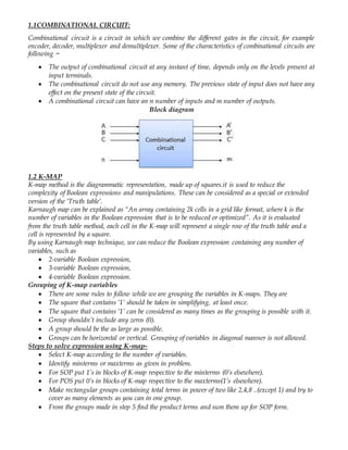
- 1. 1.1COMBINATIONAL CIRCUIT: Combinational circuit is a circuit in which we combine the different gates in the circuit, for example encoder, decoder, multiplexer and demultiplexer. Some of the characteristics of combinational circuits are following − The output of combinational circuit at any instant of time, depends only on the levels present at input terminals. The combinational circuit do not use any memory. The previous state of input does not have any effect on the present state of the circuit. A combinational circuit can have an n number of inputs and m number of outputs. Block diagram 1.2 K-MAP K-map method is the diagrammatic representation, made up of squares.it is used to reduce the complexity of Boolean expressions and manipulations. These can be considered as a special or extended version of the ‘Truth table’. Karnaugh map can be explained as “An array containing 2k cells in a grid like format, where k is the number of variables in the Boolean expression that is to be reduced or optimized”. As it is evaluated from the truth table method, each cell in the K-map will represent a single row of the truth table and a cell is represented by a square. By using Karnaugh map technique, we can reduce the Boolean expression containing any number of variables, such as 2-variable Boolean expression, 3-variable Boolean expression, 4-variable Boolean expression. Grouping of K-map variables There are some rules to follow while we are grouping the variables in K-maps. They are The square that contains ‘1’ should be taken in simplifying, at least once. The square that contains ‘1’ can be considered as many times as the grouping is possible with it. Group shouldn’t include any zeros (0). A group should be the as large as possible. Groups can be horizontal or vertical. Grouping of variables in diagonal manner is not allowed. Steps to solve expression using K-map- Select K-map according to the number of variables. Identify minterms or maxterms as given in problem. For SOP put 1’s in blocks of K-map respective to the minterms (0’s elsewhere). For POS put 0’s in blocks of K-map respective to the maxterms(1’s elsewhere). Make rectangular groups containing total terms in power of two like 2,4,8 ..(except 1) and try to cover as many elements as you can in one group. From the groups made in step 5 find the product terms and sum them up for SOP form.
- 2. SOP FORM : 2 variable K-maps There are 4 cells (22) in the 2-variable k-map. For example:F(A,B)=∑𝒎(𝟎,𝟑) equ 1= 𝑨 ̅. 𝑩 ̅ equ 2=A.B output- Y=𝑨 ̅. 𝑩 ̅+ A.B 3 variable K-maps For a 3-variable Boolean function, there is a possibility of 8 output min terms. The general representation of all the min terms using 3-variables is shown below. For example: F(A,B,C)=∑𝑚(0,1,2,3,7) Equ 1=𝑨 ̅𝑩 ̅𝑪 ̅ + 𝑨 ̅ 𝑩 ̅ 𝑪 + 𝑨 ̅ 𝑩𝑪 + 𝑨 ̅ 𝑩 𝑪 ̅ Equ 2=𝑨 ̅ 𝑩𝑪+ 𝑨𝑩𝑪 Output-Y=𝑨 ̅ + 𝑩𝑪 4 variable K-maps There are 16 possible min terms in case of a 4-variable Boolean function. The general representation of minterms using 4 variables is shown below. F(A,B,C,D)=∑m(0,2,5,7,8,10,15) Equ I=𝑨 ̅𝑩𝑪 ̅𝑫 + 𝑨 ̅ 𝑩 ̅ 𝑪𝑫 Equ II=𝑨 ̅𝑩𝑪𝑫 + 𝑨𝑩𝑪𝑫 Equ III=𝐴̅𝐵 ̅𝐶̅𝐷 ̅ +𝐴̅𝐵 ̅𝐶𝐷 ̅+𝐴𝐵 ̅𝐶̅𝐷 ̅+𝐴𝐵 ̅𝐶𝐷 ̅ OUTPUT Y=𝑨 ̅𝑩𝑫 + 𝑩𝑪𝑫 + 𝑩 ̅𝑫 ̅
- 3. POS FORM : K-map of 3 variables – F(A,B,C)=𝜋(0,3,6,7) Final expression –(A' + B’) (B’ + C’) (A + B + C) 2. K-map of 4 variables – F(A,B,C,D)=𝜋(3,5,7,8,10,11,12,13) Finally we express these as product –(C+D’+B’).(C’+D’+A).(A’+C+D).(A’+B+C’) PITFALL– Always remember POS ≠ (SOP)’ 1.3 ANALYSIS AND DESIGN PROCEDURE OF COMBINATIONAL CIRCUITS: To design of combinational circuits, the procedure involves the following steps: 1. Find the required number of inputs and outputs and assign a symbol to each. 2. Derive the truth table according to given specifications and function.
- 4. 3. Using the truth table, obtain simplified Boolean functions for each output as a function of the input variables. 4. Draw the logic circuit diagram. To obtain the output Boolean functions from a logic diagram, the procedure involves the following steps: 1. Label all gate outputs with unique symbols. 2. Find the Boolean functions for these gates. To obtain the truth table directly from the logic diagram, the procedure involves the following steps: 1. Determine the number of input variables in the circuit. 2. Draw the table for these inputs. There are 2^n combinations for the n input variables (0 to (2^n -1)). 3. Label the outputs with unique symbols for gates in the circuit. 4. Obtain the outputs of these gates in the table. Drawbacks of Combinational circuits: If you need to design a system that stores and uses previous input and output, then we can not use a combinational circuit because it doesn’t have capability to store any state or depend clock or and time. For these properties you can use Sequential circuits. Example: F2 = AB + AC + BC; T1 = A + B + C; T2 = ABC; T3 = F2’T1; F1 = T3 + T2 F1 = T3 + T2 = F2’T1 + ABC = A’BC’ + A’B’C + AB’C’ + ABC 1.4 ADDERS Adders are the basic building blocks of all arithmetic circuits; adders add two binary numbers andgive out sum and carry as output. Basically we have two types of adders. Half Adder. Full Adder. Half Adder A half-adder is an arithmetic circuit block that can be used to add two bits. Such a circuit thus has two inputs that represent the two bits to be added and two outputs, with one producing the SUM output
- 5. and the other producing the CARRY Adding two single-bit binary values X, Y produces a sum S bit and a carry out C-out bit. This operation is called half addition and thus the circuit to realize it is called a half adder The expression for the sum and carry are, 𝑆𝑢𝑚 = X ̅ 𝑌 + X𝑌 ̅ 𝑆𝑢𝑚 = X 𝑌 𝐶𝑎𝑟𝑟𝑦 = X𝑌 FULL ADDER A full adder circuit is an arithmetic circuit block that can be used to add three bits to produce a SUM anda CARRY output. Such a building block becomes a necessity when it comes to adding binary numbers with a large number of bits. The full adder circuit overcomes the limitation of the half-adder, which canbe used to add two bits only. Full adder takes a three-bits input. Adding two single-bit binary values X, Y with a carry input bit C-inproduces a sum bit S and a carry out C. 𝑆𝑢𝑚 = X ̅ 𝑌 ̅ 𝑍 + X𝑌 ̅ 𝑍̅ + X ̅ 𝑌𝑍̅ + X𝑌𝑍 𝐶𝑎𝑟𝑟𝑦 = X𝑌 + X𝑍 + 𝑌𝑍 𝑆𝑢𝑚 = X 𝑌 𝑍 X Y SUM CARRY 0 0 0 0 0 1 1 0 1 0 1 0 1 1 0 1 X Y Z SUM CARRY 0 0 0 0 0 0 0 1 1 0 0 1 0 1 0 0 1 1 0 1 1 0 0 1 0 1 0 1 0 1 1 1 0 0 1 1 1 1 1 1
- 6. SUBTRACTOR Subtractor circuits take two binary numbers as input and subtract one binary number input from the other binary number input. Similar to adders, it gives out two outputs, difference and borrow (carry-in the case of Adder). The BORROW output here specifies whether a ‗1‘ has been borrowed to perform thesubtraction. There are two types of subtractors, Half subtractor Full subtractor Half Subtractor The half-subtractor is a combinational circuit which is used to perform subtraction of two bits. It has two inputs, X (minuend) and Y (subtrahend) and two outputs D (difference) and B (borrow). The logic symbol and truth table are shown below. From the above table we can draw the K-map as shown below for "difference" and "borrow". The Boolean expression for the difference and Borrow can be written. From the equation we can draw the half-subtractor as shown in the figure below Full Subtractor A full subtractor is a combinational circuit that performs subtraction involving three bits, namely minuend, subtrahend, and borrow-in. There are two outputs, namely the DIFFERENCE output D and the BORROW output Bo. The BORROW output bit tells whether the minuend bit needs to borrow a ‗1‘ from the next possible higher minuend bit. The logic symbol and truth table are shown below. X Y D B 0 0 0 0 0 1 1 1 1 0 1 0 1 1 0 0
- 7. From the above expression, we can draw the circuit below. If you look carefully, you will see that a full-subtractor circuit is more or less same as a full-adder with slight modification. X Y Bin D Bout 0 0 0 0 0 0 0 1 1 1 0 1 0 1 1 0 1 1 0 1 1 0 0 1 0 1 0 1 0 0 1 1 0 0 0 1 1 1 1 1