SlideShare a Scribd company logo
1 of 23
Download to read offline
Prof.Satheesh MB
Indian Navy 1
ECL 315 – ANALOG INTEGRATED
CIRCUITS
COURSE : 87 INAC -L
TERM : VII
06 Jan.2014 2
TOPIC-I
IC FABRICATION
ST 2014 3
An integrated circuit (IC) is a miniature ,low cost
electronic circuit consisting of active and passive components
fabricated together on a single crystal of silicon. The active
components are transistors and diodes and passive
components are resistors and capacitors.
INTEGRATED CIRCUITS
4
Advantages of integrated circuits
1. Miniaturization and hence increased
equipment density.
2. Cost reduction due to batch processing.
3. Increased system reliability due to the
elimination of soldered joints.
4. Improved functional performance.
5. Matched devices.
6. Increased operating speeds.
7. Reduction in power consumption
5
Basic processes involved in fabricating
Monolithic ICs
1. Silicon wafer (substrate) preparation
2. Epitaxial growth
3. Oxidation
4. Photolithography
5. Diffusion
6. Ion implantation
7. Isolation technique
8. Metallization
9. Assembly processing & packaging
6
Silicon wafer (substrate) preparation
1.Crystal growth &doping
2.Ingot trimming & grinding
3.Ingot slicing
4.Wafer policing & etching
5.Wafer cleaning
Typical wafer
7
Epitaxial growth
1. Epitaxy means growing a single crystal silicon
structure upon a original silicon substrate, so that
the resulting layer is an extension of the substrate
crystal structure.
2. The basic chemical reaction in the epitaxial
growth process of pure silicon is the hydrogen
reduction of silicon tetrachloride.
1200o
C
SiCl+ 2H <-----------> Si + 4 HCl
8
Oxidation
1. SiO2 is an extremely hard protective coating & is
unaffected by almost all reagents except by
hydrochloric acid. Thus it stands against any
contamination.
2. By selective etching of SiO2, diffusion of impurities
through carefully defined through windows in the
SiO2 can be accomplished to fabricate various
components.
9
Oxidation
The silicon wafers are stacked up in a quartz boat & then
inserted into quartz furnace tube. The Si wafers are raised to
a high temperature in the range of 950 to 1150 o
C & at the
same time, exposed to a gas containing O2 or H2O or both.
The chemical action is Si + 2H2
O-----------> SiO2+ 2H2
11
Photolithography
The process of photolithography
makes it possible to produce microscopically
small circuit and device pattern on si wafer.
Two processes involved in photolithography
a) Making a photographic mask
b) Photo etching
12
Photographic mask
The development of photographic mask
involves the preparation of initial artwork and its
diffusion, reduction, decomposition of initial
artwork or layout into several mask layers.
Photo etching
Photo etching is used for the removal of SiO2
from desired regions so that the desired
impurities can be diffused.
PROCESS DIAGRAM
14
Diffusion
The process of introducing impurities into selected
regions of a silicon wafer is called diffusion. The rate at
which various impurities diffuse into the silicon will be
of the order of 1µm/hr at the temperature range of 9000
C to 11000
C .The impurity atoms have the tendency to
move from regions of higher concentrations to lower
concentrations.
15
Ion implantation technique
1. It is performed at low temperature. Therefore,
previously diffused regions have a lesser
tendency for lateral spreading.
2. In diffusion process, temperature has to be
controlled over a large area inside the oven,
where as in ion implantation process,
accelerating potential & beam content are
controlled from outside.
ION IMPLANTATION
17
Dielectric isolation
In dielectric isolation, a layer of solid
dielectric such as SiO2 or ruby completely surrounds
each components thereby producing isolation, both
electrical & physical. This isolating dielectric layer is
thick enough so that its associated capacitance is
negligible. Also, it is possible to fabricate both pnp &
npn transistors within the same silicon substrate.
18
Metalization
The process of producing a thin metal film layer that
will serve to make interconnection of the various
components on the chip is called metalization.
19
Aluminum is preferred for
metalization...?
1. It is a good conductor
2. It is easy to deposit aluminum films using vacuum
deposition.
3. It makes good mechanical bonds with silicon
4. It forms a low resistance contact.
20
IC packages
1. Metal can package.
2. Dual-in-line package.
3. Ceramic flat package.
RESISTOR FABRICATION
DIODE FABRICATION
TRANSISTOR FABRICATION

More Related Content

What's hot

n-MOS Fabrication Process
n-MOS Fabrication Processn-MOS Fabrication Process
n-MOS Fabrication ProcessSemiDesign System
 
Lecture3 IC fabrication process
Lecture3 IC fabrication processLecture3 IC fabrication process
Lecture3 IC fabrication processsritulasiadigopula
 
Fabrication of Semiconductors
Fabrication of SemiconductorsFabrication of Semiconductors
Fabrication of Semiconductorsaman1312
 
VLSI Design(Fabrication)
VLSI Design(Fabrication)VLSI Design(Fabrication)
VLSI Design(Fabrication)Trijit Mallick
 
Masking and lithography techniques
Masking and lithography techniquesMasking and lithography techniques
Masking and lithography techniquesNivethaBalu5
 
Vlsi design and fabrication ppt
Vlsi design and fabrication  pptVlsi design and fabrication  ppt
Vlsi design and fabrication pptManjushree Mashal
 
Fabrication steps of IC
Fabrication steps of ICFabrication steps of IC
Fabrication steps of ICGowri Kishore
 
Fabrication process of Integrated Circuit (IC's)
Fabrication process of Integrated Circuit (IC's)Fabrication process of Integrated Circuit (IC's)
Fabrication process of Integrated Circuit (IC's)COMSATS Abbottabad
 
Wafer Fabrication, CZ Method--ABU SYED KUET
Wafer Fabrication, CZ Method--ABU SYED KUETWafer Fabrication, CZ Method--ABU SYED KUET
Wafer Fabrication, CZ Method--ABU SYED KUETA. S. M. Jannatul Islam
 
Cmos fabrication
Cmos fabricationCmos fabrication
Cmos fabricationjigyashamaru
 
Introduction to VLSI
Introduction to VLSIIntroduction to VLSI
Introduction to VLSIShams Tabrej
 
Wafer preparation
Wafer preparationWafer preparation
Wafer preparationSomitSamanto1
 
Lecture 2 ic fabrication processing & wafer preparation
Lecture 2 ic fabrication processing & wafer preparationLecture 2 ic fabrication processing & wafer preparation
Lecture 2 ic fabrication processing & wafer preparationDr. Ghanshyam Singh
 
Device isolation Techniques
Device isolation TechniquesDevice isolation Techniques
Device isolation TechniquesSudhanshu Janwadkar
 
MOSFET fabrication 12
MOSFET fabrication 12MOSFET fabrication 12
MOSFET fabrication 12HIMANSHU DIWAKAR
 
Metal semiconductor contacts
Metal semiconductor contactsMetal semiconductor contacts
Metal semiconductor contactsKasif Nabi
 

What's hot (20)

n-MOS Fabrication Process
n-MOS Fabrication Processn-MOS Fabrication Process
n-MOS Fabrication Process
 
Lecture3 IC fabrication process
Lecture3 IC fabrication processLecture3 IC fabrication process
Lecture3 IC fabrication process
 
Fabrication of Semiconductors
Fabrication of SemiconductorsFabrication of Semiconductors
Fabrication of Semiconductors
 
VLSI Design(Fabrication)
VLSI Design(Fabrication)VLSI Design(Fabrication)
VLSI Design(Fabrication)
 
Masking and lithography techniques
Masking and lithography techniquesMasking and lithography techniques
Masking and lithography techniques
 
MOS Capacitor
MOS CapacitorMOS Capacitor
MOS Capacitor
 
Vlsi design and fabrication ppt
Vlsi design and fabrication  pptVlsi design and fabrication  ppt
Vlsi design and fabrication ppt
 
Fabrication steps of IC
Fabrication steps of ICFabrication steps of IC
Fabrication steps of IC
 
Fabrication process of Integrated Circuit (IC's)
Fabrication process of Integrated Circuit (IC's)Fabrication process of Integrated Circuit (IC's)
Fabrication process of Integrated Circuit (IC's)
 
Metallization
MetallizationMetallization
Metallization
 
Wafer Fabrication, CZ Method--ABU SYED KUET
Wafer Fabrication, CZ Method--ABU SYED KUETWafer Fabrication, CZ Method--ABU SYED KUET
Wafer Fabrication, CZ Method--ABU SYED KUET
 
Cmos fabrication
Cmos fabricationCmos fabrication
Cmos fabrication
 
Introduction to VLSI
Introduction to VLSIIntroduction to VLSI
Introduction to VLSI
 
Fabrication of IC
Fabrication of ICFabrication of IC
Fabrication of IC
 
Wafer preparation
Wafer preparationWafer preparation
Wafer preparation
 
Lecture 2 ic fabrication processing & wafer preparation
Lecture 2 ic fabrication processing & wafer preparationLecture 2 ic fabrication processing & wafer preparation
Lecture 2 ic fabrication processing & wafer preparation
 
Device isolation Techniques
Device isolation TechniquesDevice isolation Techniques
Device isolation Techniques
 
Cmos process flow
Cmos process flowCmos process flow
Cmos process flow
 
MOSFET fabrication 12
MOSFET fabrication 12MOSFET fabrication 12
MOSFET fabrication 12
 
Metal semiconductor contacts
Metal semiconductor contactsMetal semiconductor contacts
Metal semiconductor contacts
 

Similar to 2.ic fabrication

Epitaxial growth
Epitaxial growthEpitaxial growth
Epitaxial growthIYPUMANI
 
VLSI Technology.pptx
VLSI Technology.pptxVLSI Technology.pptx
VLSI Technology.pptxkiran27822
 
MONOLITHIC IC PROCESSES ppt.pptx
MONOLITHIC IC PROCESSES ppt.pptxMONOLITHIC IC PROCESSES ppt.pptx
MONOLITHIC IC PROCESSES ppt.pptxParasSingh894545
 
SILICON ON INSULATOR
SILICON ON INSULATORSILICON ON INSULATOR
SILICON ON INSULATORManishKushwaha60
 
Monolithic implementation of parasitic elements
Monolithic implementation of parasitic elementsMonolithic implementation of parasitic elements
Monolithic implementation of parasitic elementsGOPICHAND NAGUBOINA
 
microfabrication-180118174836 (1).pdf
microfabrication-180118174836 (1).pdfmicrofabrication-180118174836 (1).pdf
microfabrication-180118174836 (1).pdfSenguttuvan Nagarajan
 
Planar fabrication technology
Planar fabrication technologyPlanar fabrication technology
Planar fabrication technologyPrathamesh Gardi
 
Unit-6 Semiconductor Manufacturing Process.pptx
Unit-6 Semiconductor Manufacturing Process.pptxUnit-6 Semiconductor Manufacturing Process.pptx
Unit-6 Semiconductor Manufacturing Process.pptxSatish Chandra
 
Making of a silicon chip
Making of a silicon chipMaking of a silicon chip
Making of a silicon chipsurabhi8
 
Vlsi assembly technology
Vlsi  assembly technologyVlsi  assembly technology
Vlsi assembly technologyAshu0711
 
IJSRED-V2I4P3
IJSRED-V2I4P3IJSRED-V2I4P3
IJSRED-V2I4P3IJSRED
 
Xaioling Ding-NM
Xaioling Ding-NMXaioling Ding-NM
Xaioling Ding-NMDavid Edwards
 
Integrated circuits ic
Integrated circuits ic Integrated circuits ic
Integrated circuits ic Rishi Kumar Jha
 
Introduction To Microelectronics
Introduction To MicroelectronicsIntroduction To Microelectronics
Introduction To MicroelectronicsAnkita Jaiswal
 
IC design: Microelectronic Technology.pptx
IC design: Microelectronic Technology.pptxIC design: Microelectronic Technology.pptx
IC design: Microelectronic Technology.pptxSarmistaSengupta1
 
3_DVD_IC_Fabrication_Flow_designer_perspective.pdf
3_DVD_IC_Fabrication_Flow_designer_perspective.pdf3_DVD_IC_Fabrication_Flow_designer_perspective.pdf
3_DVD_IC_Fabrication_Flow_designer_perspective.pdfUsha Mehta
 

Similar to 2.ic fabrication (20)

Epitaxial growth
Epitaxial growthEpitaxial growth
Epitaxial growth
 
VLSI Technology.pptx
VLSI Technology.pptxVLSI Technology.pptx
VLSI Technology.pptx
 
MONOLITHIC IC PROCESSES ppt.pptx
MONOLITHIC IC PROCESSES ppt.pptxMONOLITHIC IC PROCESSES ppt.pptx
MONOLITHIC IC PROCESSES ppt.pptx
 
SILICON ON INSULATOR
SILICON ON INSULATORSILICON ON INSULATOR
SILICON ON INSULATOR
 
Monolithic implementation of parasitic elements
Monolithic implementation of parasitic elementsMonolithic implementation of parasitic elements
Monolithic implementation of parasitic elements
 
microfabrication-180118174836 (1).pdf
microfabrication-180118174836 (1).pdfmicrofabrication-180118174836 (1).pdf
microfabrication-180118174836 (1).pdf
 
Planar fabrication technology
Planar fabrication technologyPlanar fabrication technology
Planar fabrication technology
 
Unit-6 Semiconductor Manufacturing Process.pptx
Unit-6 Semiconductor Manufacturing Process.pptxUnit-6 Semiconductor Manufacturing Process.pptx
Unit-6 Semiconductor Manufacturing Process.pptx
 
Making of a silicon chip
Making of a silicon chipMaking of a silicon chip
Making of a silicon chip
 
Oxidation--ABU SYED KUET
Oxidation--ABU SYED KUETOxidation--ABU SYED KUET
Oxidation--ABU SYED KUET
 
Vlsi assembly technology
Vlsi  assembly technologyVlsi  assembly technology
Vlsi assembly technology
 
Ic fab
Ic fabIc fab
Ic fab
 
IJSRED-V2I4P3
IJSRED-V2I4P3IJSRED-V2I4P3
IJSRED-V2I4P3
 
REPORT
REPORTREPORT
REPORT
 
Xaioling Ding-NM
Xaioling Ding-NMXaioling Ding-NM
Xaioling Ding-NM
 
Integrated circuits ic
Integrated circuits ic Integrated circuits ic
Integrated circuits ic
 
Introduction To Microelectronics
Introduction To MicroelectronicsIntroduction To Microelectronics
Introduction To Microelectronics
 
Ue 1(v sem)
Ue 1(v sem)Ue 1(v sem)
Ue 1(v sem)
 
IC design: Microelectronic Technology.pptx
IC design: Microelectronic Technology.pptxIC design: Microelectronic Technology.pptx
IC design: Microelectronic Technology.pptx
 
3_DVD_IC_Fabrication_Flow_designer_perspective.pdf
3_DVD_IC_Fabrication_Flow_designer_perspective.pdf3_DVD_IC_Fabrication_Flow_designer_perspective.pdf
3_DVD_IC_Fabrication_Flow_designer_perspective.pdf
 

More from INDIAN NAVY

RECENT TRENDS IN COMMUNICATION AND APPLICATIONS
RECENT TRENDS IN COMMUNICATION AND APPLICATIONSRECENT TRENDS IN COMMUNICATION AND APPLICATIONS
RECENT TRENDS IN COMMUNICATION AND APPLICATIONSINDIAN NAVY
 
EMI/EMC in Mobile Communication
EMI/EMC in Mobile CommunicationEMI/EMC in Mobile Communication
EMI/EMC in Mobile CommunicationINDIAN NAVY
 
RECENT TRENDS AND OPPORTUNITIES IN TELECOMMUNICATION
RECENT TRENDS AND OPPORTUNITIES IN TELECOMMUNICATIONRECENT TRENDS AND OPPORTUNITIES IN TELECOMMUNICATION
RECENT TRENDS AND OPPORTUNITIES IN TELECOMMUNICATIONINDIAN NAVY
 
Scheduling Algorithms in LTE and Future Cellular Networks
Scheduling Algorithms in LTE and Future Cellular NetworksScheduling Algorithms in LTE and Future Cellular Networks
Scheduling Algorithms in LTE and Future Cellular NetworksINDIAN NAVY
 
1.1.Operations on signals
1.1.Operations on signals1.1.Operations on signals
1.1.Operations on signalsINDIAN NAVY
 
8.ic555 timer volt regulator
8.ic555 timer volt regulator8.ic555 timer volt regulator
8.ic555 timer volt regulatorINDIAN NAVY
 
7.instrumentation amplifier
7.instrumentation amplifier7.instrumentation amplifier
7.instrumentation amplifierINDIAN NAVY
 
3.ic opamp
3.ic opamp3.ic opamp
3.ic opampINDIAN NAVY
 
4.Sampling and Hilbert Transform
4.Sampling and Hilbert Transform4.Sampling and Hilbert Transform
4.Sampling and Hilbert TransformINDIAN NAVY
 
3.Frequency Domain Representation of Signals and Systems
3.Frequency Domain Representation of Signals and Systems3.Frequency Domain Representation of Signals and Systems
3.Frequency Domain Representation of Signals and SystemsINDIAN NAVY
 
2.time domain analysis of lti systems
2.time domain analysis of lti systems2.time domain analysis of lti systems
2.time domain analysis of lti systemsINDIAN NAVY
 
1.introduction to signals
1.introduction to signals1.introduction to signals
1.introduction to signalsINDIAN NAVY
 
Lte Evolution and Basics
Lte Evolution and BasicsLte Evolution and Basics
Lte Evolution and BasicsINDIAN NAVY
 
7.Active Filters using Opamp
7.Active Filters using Opamp7.Active Filters using Opamp
7.Active Filters using OpampINDIAN NAVY
 
4.Basics of systems
4.Basics of systems4.Basics of systems
4.Basics of systemsINDIAN NAVY
 
2.Opamp parameters
2.Opamp parameters2.Opamp parameters
2.Opamp parametersINDIAN NAVY
 
3.Properties of signals
3.Properties of signals3.Properties of signals
3.Properties of signalsINDIAN NAVY
 
1.Basics of Signals
1.Basics of Signals1.Basics of Signals
1.Basics of SignalsINDIAN NAVY
 
1.Operational Amplifier
1.Operational Amplifier1.Operational Amplifier
1.Operational AmplifierINDIAN NAVY
 
Linear IC Technology
Linear IC TechnologyLinear IC Technology
Linear IC TechnologyINDIAN NAVY
 

More from INDIAN NAVY (20)

RECENT TRENDS IN COMMUNICATION AND APPLICATIONS
RECENT TRENDS IN COMMUNICATION AND APPLICATIONSRECENT TRENDS IN COMMUNICATION AND APPLICATIONS
RECENT TRENDS IN COMMUNICATION AND APPLICATIONS
 
EMI/EMC in Mobile Communication
EMI/EMC in Mobile CommunicationEMI/EMC in Mobile Communication
EMI/EMC in Mobile Communication
 
RECENT TRENDS AND OPPORTUNITIES IN TELECOMMUNICATION
RECENT TRENDS AND OPPORTUNITIES IN TELECOMMUNICATIONRECENT TRENDS AND OPPORTUNITIES IN TELECOMMUNICATION
RECENT TRENDS AND OPPORTUNITIES IN TELECOMMUNICATION
 
Scheduling Algorithms in LTE and Future Cellular Networks
Scheduling Algorithms in LTE and Future Cellular NetworksScheduling Algorithms in LTE and Future Cellular Networks
Scheduling Algorithms in LTE and Future Cellular Networks
 
1.1.Operations on signals
1.1.Operations on signals1.1.Operations on signals
1.1.Operations on signals
 
8.ic555 timer volt regulator
8.ic555 timer volt regulator8.ic555 timer volt regulator
8.ic555 timer volt regulator
 
7.instrumentation amplifier
7.instrumentation amplifier7.instrumentation amplifier
7.instrumentation amplifier
 
3.ic opamp
3.ic opamp3.ic opamp
3.ic opamp
 
4.Sampling and Hilbert Transform
4.Sampling and Hilbert Transform4.Sampling and Hilbert Transform
4.Sampling and Hilbert Transform
 
3.Frequency Domain Representation of Signals and Systems
3.Frequency Domain Representation of Signals and Systems3.Frequency Domain Representation of Signals and Systems
3.Frequency Domain Representation of Signals and Systems
 
2.time domain analysis of lti systems
2.time domain analysis of lti systems2.time domain analysis of lti systems
2.time domain analysis of lti systems
 
1.introduction to signals
1.introduction to signals1.introduction to signals
1.introduction to signals
 
Lte Evolution and Basics
Lte Evolution and BasicsLte Evolution and Basics
Lte Evolution and Basics
 
7.Active Filters using Opamp
7.Active Filters using Opamp7.Active Filters using Opamp
7.Active Filters using Opamp
 
4.Basics of systems
4.Basics of systems4.Basics of systems
4.Basics of systems
 
2.Opamp parameters
2.Opamp parameters2.Opamp parameters
2.Opamp parameters
 
3.Properties of signals
3.Properties of signals3.Properties of signals
3.Properties of signals
 
1.Basics of Signals
1.Basics of Signals1.Basics of Signals
1.Basics of Signals
 
1.Operational Amplifier
1.Operational Amplifier1.Operational Amplifier
1.Operational Amplifier
 
Linear IC Technology
Linear IC TechnologyLinear IC Technology
Linear IC Technology
 

Recently uploaded

How to Make a Pirate ship Primary Education.pptx
How to Make a Pirate ship Primary Education.pptxHow to Make a Pirate ship Primary Education.pptx
How to Make a Pirate ship Primary Education.pptxmanuelaromero2013
 
POINT- BIOCHEMISTRY SEM 2 ENZYMES UNIT 5.pptx
POINT- BIOCHEMISTRY SEM 2 ENZYMES UNIT 5.pptxPOINT- BIOCHEMISTRY SEM 2 ENZYMES UNIT 5.pptx
POINT- BIOCHEMISTRY SEM 2 ENZYMES UNIT 5.pptxSayali Powar
 
Hierarchy of management that covers different levels of management
Hierarchy of management that covers different levels of managementHierarchy of management that covers different levels of management
Hierarchy of management that covers different levels of managementmkooblal
 
ECONOMIC CONTEXT - PAPER 1 Q3: NEWSPAPERS.pptx
ECONOMIC CONTEXT - PAPER 1 Q3: NEWSPAPERS.pptxECONOMIC CONTEXT - PAPER 1 Q3: NEWSPAPERS.pptx
ECONOMIC CONTEXT - PAPER 1 Q3: NEWSPAPERS.pptxiammrhaywood
 
Introduction to ArtificiaI Intelligence in Higher Education
Introduction to ArtificiaI Intelligence in Higher EducationIntroduction to ArtificiaI Intelligence in Higher Education
Introduction to ArtificiaI Intelligence in Higher Educationpboyjonauth
 
MARGINALIZATION (Different learners in Marginalized Group
MARGINALIZATION (Different learners in Marginalized GroupMARGINALIZATION (Different learners in Marginalized Group
MARGINALIZATION (Different learners in Marginalized GroupJonathanParaisoCruz
 
Meghan Sutherland In Media Res Media Component
Meghan Sutherland In Media Res Media ComponentMeghan Sutherland In Media Res Media Component
Meghan Sutherland In Media Res Media ComponentInMediaRes1
 
Introduction to AI in Higher Education_draft.pptx
Introduction to AI in Higher Education_draft.pptxIntroduction to AI in Higher Education_draft.pptx
Introduction to AI in Higher Education_draft.pptxpboyjonauth
 
Alper Gobel In Media Res Media Component
Alper Gobel In Media Res Media ComponentAlper Gobel In Media Res Media Component
Alper Gobel In Media Res Media ComponentInMediaRes1
 
Proudly South Africa powerpoint Thorisha.pptx
Proudly South Africa powerpoint Thorisha.pptxProudly South Africa powerpoint Thorisha.pptx
Proudly South Africa powerpoint Thorisha.pptxthorishapillay1
 
Framing an Appropriate Research Question 6b9b26d93da94caf993c038d9efcdedb.pdf
Framing an Appropriate Research Question 6b9b26d93da94caf993c038d9efcdedb.pdfFraming an Appropriate Research Question 6b9b26d93da94caf993c038d9efcdedb.pdf
Framing an Appropriate Research Question 6b9b26d93da94caf993c038d9efcdedb.pdfUjwalaBharambe
 
18-04-UA_REPORT_MEDIALITERAСY_INDEX-DM_23-1-final-eng.pdf
18-04-UA_REPORT_MEDIALITERAСY_INDEX-DM_23-1-final-eng.pdf18-04-UA_REPORT_MEDIALITERAСY_INDEX-DM_23-1-final-eng.pdf
18-04-UA_REPORT_MEDIALITERAСY_INDEX-DM_23-1-final-eng.pdfssuser54595a
 
Capitol Tech U Doctoral Presentation - April 2024.pptx
Capitol Tech U Doctoral Presentation - April 2024.pptxCapitol Tech U Doctoral Presentation - April 2024.pptx
Capitol Tech U Doctoral Presentation - April 2024.pptxCapitolTechU
 
CELL CYCLE Division Science 8 quarter IV.pptx
CELL CYCLE Division Science 8 quarter IV.pptxCELL CYCLE Division Science 8 quarter IV.pptx
CELL CYCLE Division Science 8 quarter IV.pptxJiesonDelaCerna
 
Biting mechanism of poisonous snakes.pdf
Biting mechanism of poisonous snakes.pdfBiting mechanism of poisonous snakes.pdf
Biting mechanism of poisonous snakes.pdfadityarao40181
 
Organic Name Reactions for the students and aspirants of Chemistry12th.pptx
Organic Name Reactions  for the students and aspirants of Chemistry12th.pptxOrganic Name Reactions  for the students and aspirants of Chemistry12th.pptx
Organic Name Reactions for the students and aspirants of Chemistry12th.pptxVS Mahajan Coaching Centre
 
Full Stack Web Development Course for Beginners
Full Stack Web Development Course  for BeginnersFull Stack Web Development Course  for Beginners
Full Stack Web Development Course for BeginnersSabitha Banu
 

Recently uploaded (20)

How to Make a Pirate ship Primary Education.pptx
How to Make a Pirate ship Primary Education.pptxHow to Make a Pirate ship Primary Education.pptx
How to Make a Pirate ship Primary Education.pptx
 
POINT- BIOCHEMISTRY SEM 2 ENZYMES UNIT 5.pptx
POINT- BIOCHEMISTRY SEM 2 ENZYMES UNIT 5.pptxPOINT- BIOCHEMISTRY SEM 2 ENZYMES UNIT 5.pptx
POINT- BIOCHEMISTRY SEM 2 ENZYMES UNIT 5.pptx
 
OS-operating systems- ch04 (Threads) ...
OS-operating systems- ch04 (Threads) ...OS-operating systems- ch04 (Threads) ...
OS-operating systems- ch04 (Threads) ...
 
Hierarchy of management that covers different levels of management
Hierarchy of management that covers different levels of managementHierarchy of management that covers different levels of management
Hierarchy of management that covers different levels of management
 
ECONOMIC CONTEXT - PAPER 1 Q3: NEWSPAPERS.pptx
ECONOMIC CONTEXT - PAPER 1 Q3: NEWSPAPERS.pptxECONOMIC CONTEXT - PAPER 1 Q3: NEWSPAPERS.pptx
ECONOMIC CONTEXT - PAPER 1 Q3: NEWSPAPERS.pptx
 
Introduction to ArtificiaI Intelligence in Higher Education
Introduction to ArtificiaI Intelligence in Higher EducationIntroduction to ArtificiaI Intelligence in Higher Education
Introduction to ArtificiaI Intelligence in Higher Education
 
Model Call Girl in Tilak Nagar Delhi reach out to us at 🔝9953056974🔝
Model Call Girl in Tilak Nagar Delhi reach out to us at 🔝9953056974🔝Model Call Girl in Tilak Nagar Delhi reach out to us at 🔝9953056974🔝
Model Call Girl in Tilak Nagar Delhi reach out to us at 🔝9953056974🔝
 
MARGINALIZATION (Different learners in Marginalized Group
MARGINALIZATION (Different learners in Marginalized GroupMARGINALIZATION (Different learners in Marginalized Group
MARGINALIZATION (Different learners in Marginalized Group
 
TataKelola dan KamSiber Kecerdasan Buatan v022.pdf
TataKelola dan KamSiber Kecerdasan Buatan v022.pdfTataKelola dan KamSiber Kecerdasan Buatan v022.pdf
TataKelola dan KamSiber Kecerdasan Buatan v022.pdf
 
Meghan Sutherland In Media Res Media Component
Meghan Sutherland In Media Res Media ComponentMeghan Sutherland In Media Res Media Component
Meghan Sutherland In Media Res Media Component
 
Introduction to AI in Higher Education_draft.pptx
Introduction to AI in Higher Education_draft.pptxIntroduction to AI in Higher Education_draft.pptx
Introduction to AI in Higher Education_draft.pptx
 
Alper Gobel In Media Res Media Component
Alper Gobel In Media Res Media ComponentAlper Gobel In Media Res Media Component
Alper Gobel In Media Res Media Component
 
Proudly South Africa powerpoint Thorisha.pptx
Proudly South Africa powerpoint Thorisha.pptxProudly South Africa powerpoint Thorisha.pptx
Proudly South Africa powerpoint Thorisha.pptx
 
Framing an Appropriate Research Question 6b9b26d93da94caf993c038d9efcdedb.pdf
Framing an Appropriate Research Question 6b9b26d93da94caf993c038d9efcdedb.pdfFraming an Appropriate Research Question 6b9b26d93da94caf993c038d9efcdedb.pdf
Framing an Appropriate Research Question 6b9b26d93da94caf993c038d9efcdedb.pdf
 
18-04-UA_REPORT_MEDIALITERAСY_INDEX-DM_23-1-final-eng.pdf
18-04-UA_REPORT_MEDIALITERAСY_INDEX-DM_23-1-final-eng.pdf18-04-UA_REPORT_MEDIALITERAСY_INDEX-DM_23-1-final-eng.pdf
18-04-UA_REPORT_MEDIALITERAСY_INDEX-DM_23-1-final-eng.pdf
 
Capitol Tech U Doctoral Presentation - April 2024.pptx
Capitol Tech U Doctoral Presentation - April 2024.pptxCapitol Tech U Doctoral Presentation - April 2024.pptx
Capitol Tech U Doctoral Presentation - April 2024.pptx
 
CELL CYCLE Division Science 8 quarter IV.pptx
CELL CYCLE Division Science 8 quarter IV.pptxCELL CYCLE Division Science 8 quarter IV.pptx
CELL CYCLE Division Science 8 quarter IV.pptx
 
Biting mechanism of poisonous snakes.pdf
Biting mechanism of poisonous snakes.pdfBiting mechanism of poisonous snakes.pdf
Biting mechanism of poisonous snakes.pdf
 
Organic Name Reactions for the students and aspirants of Chemistry12th.pptx
Organic Name Reactions  for the students and aspirants of Chemistry12th.pptxOrganic Name Reactions  for the students and aspirants of Chemistry12th.pptx
Organic Name Reactions for the students and aspirants of Chemistry12th.pptx
 
Full Stack Web Development Course for Beginners
Full Stack Web Development Course  for BeginnersFull Stack Web Development Course  for Beginners
Full Stack Web Development Course for Beginners
 

2.ic fabrication

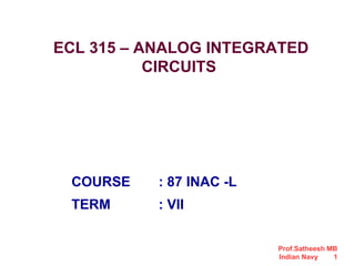
  • 1. Prof.Satheesh MB Indian Navy 1 ECL 315 – ANALOG INTEGRATED CIRCUITS COURSE : 87 INAC -L TERM : VII
  • 3. ST 2014 3 An integrated circuit (IC) is a miniature ,low cost electronic circuit consisting of active and passive components fabricated together on a single crystal of silicon. The active components are transistors and diodes and passive components are resistors and capacitors. INTEGRATED CIRCUITS
  • 4. 4 Advantages of integrated circuits 1. Miniaturization and hence increased equipment density. 2. Cost reduction due to batch processing. 3. Increased system reliability due to the elimination of soldered joints. 4. Improved functional performance. 5. Matched devices. 6. Increased operating speeds. 7. Reduction in power consumption
  • 5. 5 Basic processes involved in fabricating Monolithic ICs 1. Silicon wafer (substrate) preparation 2. Epitaxial growth 3. Oxidation 4. Photolithography 5. Diffusion 6. Ion implantation 7. Isolation technique 8. Metallization 9. Assembly processing & packaging
  • 6. 6 Silicon wafer (substrate) preparation 1.Crystal growth &doping 2.Ingot trimming & grinding 3.Ingot slicing 4.Wafer policing & etching 5.Wafer cleaning Typical wafer
  • 7. 7 Epitaxial growth 1. Epitaxy means growing a single crystal silicon structure upon a original silicon substrate, so that the resulting layer is an extension of the substrate crystal structure. 2. The basic chemical reaction in the epitaxial growth process of pure silicon is the hydrogen reduction of silicon tetrachloride. 1200o C SiCl+ 2H <-----------> Si + 4 HCl
  • 8. 8 Oxidation 1. SiO2 is an extremely hard protective coating & is unaffected by almost all reagents except by hydrochloric acid. Thus it stands against any contamination. 2. By selective etching of SiO2, diffusion of impurities through carefully defined through windows in the SiO2 can be accomplished to fabricate various components.
  • 9. 9 Oxidation The silicon wafers are stacked up in a quartz boat & then inserted into quartz furnace tube. The Si wafers are raised to a high temperature in the range of 950 to 1150 o C & at the same time, exposed to a gas containing O2 or H2O or both. The chemical action is Si + 2H2 O-----------> SiO2+ 2H2
  • 10.
  • 11. 11 Photolithography The process of photolithography makes it possible to produce microscopically small circuit and device pattern on si wafer. Two processes involved in photolithography a) Making a photographic mask b) Photo etching
  • 12. 12 Photographic mask The development of photographic mask involves the preparation of initial artwork and its diffusion, reduction, decomposition of initial artwork or layout into several mask layers. Photo etching Photo etching is used for the removal of SiO2 from desired regions so that the desired impurities can be diffused.
  • 14. 14 Diffusion The process of introducing impurities into selected regions of a silicon wafer is called diffusion. The rate at which various impurities diffuse into the silicon will be of the order of 1µm/hr at the temperature range of 9000 C to 11000 C .The impurity atoms have the tendency to move from regions of higher concentrations to lower concentrations.
  • 15. 15 Ion implantation technique 1. It is performed at low temperature. Therefore, previously diffused regions have a lesser tendency for lateral spreading. 2. In diffusion process, temperature has to be controlled over a large area inside the oven, where as in ion implantation process, accelerating potential & beam content are controlled from outside.
  • 17. 17 Dielectric isolation In dielectric isolation, a layer of solid dielectric such as SiO2 or ruby completely surrounds each components thereby producing isolation, both electrical & physical. This isolating dielectric layer is thick enough so that its associated capacitance is negligible. Also, it is possible to fabricate both pnp & npn transistors within the same silicon substrate.
  • 18. 18 Metalization The process of producing a thin metal film layer that will serve to make interconnection of the various components on the chip is called metalization.
  • 19. 19 Aluminum is preferred for metalization...? 1. It is a good conductor 2. It is easy to deposit aluminum films using vacuum deposition. 3. It makes good mechanical bonds with silicon 4. It forms a low resistance contact.
  • 20. 20 IC packages 1. Metal can package. 2. Dual-in-line package. 3. Ceramic flat package.