Integrated circuits ic
•
0 likes•355 views

Integrated circuits are formed on small silicon chips and can be categorized based on the number of logic gates as SSI, MSI, LSI, VLSI, or ULSI. The fabrication process involves growing layers on the silicon wafer through steps like epitaxial growth, oxidation, photolithography, diffusion, and metallization to connect components. Photolithography is a key step where a light-sensitive photo-resist is used to selectively expose and remove silicon dioxide, allowing impurities to be introduced to create different circuit components on the chip.

Recommended
More Related Content
What's hot
What's hot (19)
Similar to Integrated circuits ic
Similar to Integrated circuits ic (20)
Recently uploaded
Recently uploaded (20)
Integrated circuits ic
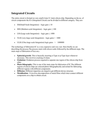
- 1. Integrated Circuits The entire circuit is formed on very small (1mm X 1mm) silicon chip. Depending on the no. of circuit components the ICs (Integrated Circuit) can be divided in different category. They are- SSI(Small Scale Integration) – logic gate ≤ 10 MSI (Medium scale Integration) – logic gate ≤ 100 LSI (Large scale Integration) – logic gate ≤ 1000 VLSI (very large scale Integration) – logic gates > 1000 ULSI (Ultra large scale Integration) logic gates > 1000000 The technology of fabrication IC is a very expensive and very vast. Here briefly we are describing the process.The process starts with silicon wafer followed by the different steps. The main steps of fabrication of Ices are,- Epitaxial growth: This is basically inserting n-Type or p-Type layer whenever necessary. This involves cracking of silane. Oxidation: Oxidation process required to separate one region of the silicon chip from other. Photo lithography: This is one of the main steps for fabrication of IC.The different regions of silicon chips are selected photo lithographically and etched for fabricating different regions with different components. Diffusion: Different impurities are doped to get different device structure. Metallization: It involves decomposition of metal films which inter-connect different components on a chip to obtain circuit.
- 3. As mention earlier Photo lithography is the main step in fabricating. Issuing this process SiO2 of some regions are removed deliberately to introduce some impurities. On the silicon chip, a thin layer of SiO2 is first deposited over which a photo-sensitive emulsion called photo-resist is coated. This has a property that exposed portion get polymerized and resist any chemical etching. By this property desired portion can get polymerized and rest will be remaining same. The chip is then dipped in solvent which dissolves the unpolymerised portion of the photo-resist. Now it is exposed to chemical etchant which removes SiO2 leaving exposed Si surface beneath it through which metallization can be carried out to get a device called circuit.