SlideShare a Scribd company logo
1 of 27
Charge-Potential
Characteristics of
MOS Capacitor
Arpan Deyasi
Dept of ECE, RCCIIT, Kolkata, India
11/3/2020 1Arpan Deyasi, RCCIIT, India
11/3/2020 Arpan Deyasi, RCCIIT, India 2
VM>0 & large
Al SiO2
Si(p)
1
2
point of
inversion
3
ΨF
ΨS
RecapitulationofInversionCondition
11/3/2020 Arpan Deyasi, RCCIIT, India 3
VM>0 & large
Al SiO2
Si(p)
1
2
point of
inversion
3
ΨF
ΨS
ClassificationofInversion
2ΨF >Ψs>ΨF
Weak inversion
11/3/2020 Arpan Deyasi, RCCIIT, India 4
VM>0 & large
Al SiO2
Si(p)
1
2
point of
inversion
3
ΨF
ΨS
ClassificationofInversion
Ψs≥2ΨF
Strong inversion
Mathematical representation of band bending
Band bending is defined
Ψ(z) = ΨI(z) - ΨI(z ∞)
Assumption
Ψ(z)>0 for downward bending
Ψ(z)<0 for downward bending
Boundary conditions
Ψ(z)=0 in bulk semiconductor
Ψ(z=0) = ΨS at SiO2-Si interface
11/3/2020 5Arpan Deyasi, RCCIIT, India
Poisson’s Equation for the Device
[ ]
2
2
( ) ( ) ( ) ( )D A
d q
p z n z N z N z
dz
ψ
ε
=− − + −
In bulk substrate, p(z)=NA
2
( ) i
A
n
n z
N
=
11/3/2020 6Arpan Deyasi, RCCIIT, India
Charge Neutrality Condition
( ) ( ) ( ) ( ) 0D Ap z n z N z N z− + − =
( )
2
( ) i
D A A
A
n
N z N z N
N
− = −
11/3/2020 7Arpan Deyasi, RCCIIT, India
Charge Variation
( ) exp ( )i F I
q
p z n
kT
 
= Ψ − Ψ  
( ) exp ( )i F
q
p z n
kT
 
= Ψ − Ψ  
11/3/2020 8Arpan Deyasi, RCCIIT, India
Charge Variation
( ) exp expi F
q q
p z n
kT kT
   
= Ψ −Ψ      
( ) expA
q
p z N
kT
 
= −Ψ  
11/3/2020 9Arpan Deyasi, RCCIIT, India
Charge Variation
( ) exp ( )i I F
q
n z n
kT
 
= Ψ − Ψ  
( ) exp ( )i F
q
n z n
kT
 
= Ψ − Ψ  
11/3/2020 10Arpan Deyasi, RCCIIT, India
Charge Variation
( ) exp expi F
q q
n z n
kT kT
   
= −Ψ Ψ      
2
( ) expi
A
n q
n z
N kT
   
= Ψ     
11/3/2020 11Arpan Deyasi, RCCIIT, India
Poisson’s Equation for the Device
2
2 22
exp
exp
A A
i i
A A
q
N N
kTd q
dz n nq
N kT N
ψ
ε
  
−Ψ −    = −
    
− Ψ +        
11/3/2020 12Arpan Deyasi, RCCIIT, India
Poisson’s Equation for the Device
2
2 2
exp 1
exp 1
A
i
A
q
N
kTd q
dz n q
N kT
ψ
ε
   
−Ψ −      = −
    − Ψ −      
11/3/2020 13Arpan Deyasi, RCCIIT, India
Solution of Poisson’s Equation
Step 2: Multiply both sides by (dΨ/dz)
Step 1: Integrate from bulk (Ψ=0)
to surface [(dΨ/dz)=0]
11/3/2020 14Arpan Deyasi, RCCIIT, India
Solution of Poisson’s Equation
2
2 2
0 0
exp 1
exp 1
d Adz
i
A
q
N
kTd q
dz n q
N kT
ψ
ε
Ψ
Ψ
   
−Ψ −      = −
    − Ψ −      
∫ ∫
11/3/2020 15Arpan Deyasi, RCCIIT, India
11/3/2020 Arpan Deyasi, RCCIIT, India 16
0
2
0
exp 1
exp 1
d
dz
A
i
A
d d q
dz dz
q
N
kT
n q
N kT
ψ
ε
Ψ
Ψ
 
=− × 
 
   
−Ψ −      
    − Ψ −      
∫
∫
Solution of Poisson’s Equation
0
2
0
exp 1
exp 1
d
dz
d Adz
i
A
d d d
dz dz dz
q
N
kTq d
dzn q
N kT
ψ ψ
ψ
ε
Ψ
Ψ
   
× =   
   
   
−Ψ −        − ×       − Ψ −      
∫
∫
11/3/2020 17Arpan Deyasi, RCCIIT, India
Solution of Poisson’s Equation
0
2
0
exp 1
exp 1
d
dz
A
i
A
d d
d
dz dz
q
N
kTq
d
n q
N kT
ψ ψ
ψ
ε
Ψ
Ψ
   
=   
   
   
−Ψ −      − ×
    − Ψ −      
∫
∫
11/3/2020 18Arpan Deyasi, RCCIIT, India
Expression of Electric Field
[ ]
2
2
2
2
2
( )
exp 1
exp 1
A
i
A
d kTN
z
dz
q q
kT kT
n q q
kT kTN
ψ
ξ
ε
 
= = × 
 
  Ψ Ψ    
− + −     
     
  Ψ Ψ    
 + − −    
      
11/3/2020 19Arpan Deyasi, RCCIIT, India
11/3/2020 20Arpan Deyasi, RCCIIT, India
Boundary condition for Electric Field
at z=0 (insulator-semiconductor interface)
[i] Ψ = ΨS
[ii] ξ = ξS
11/3/2020 Arpan Deyasi, RCCIIT, India 21
Surface Electric Field
0.5
2
2
2
exp 1
exp 1
A
S
S S
i S S
A
kTN
q q
kT kT
n q q
kT kTN
ξ
ε
= ×
  Ψ Ψ    
− + −     
     
  Ψ Ψ    
 + − −    
      
11/3/2020 Arpan Deyasi, RCCIIT, India 22
Surface Charge
From Gauss’ law S SQ εξ= −
0.5
2
2
2
exp 1
exp 1
S S A
S S
i S S
A
Q kTN
q q
kT kT
n q q
kT kTN
εξ ε=− = ×
  Ψ Ψ    
− + −     
     
  Ψ Ψ    
 + − −    
      
11/3/2020 Arpan Deyasi, RCCIIT, India 23
Graphical representation of Charge Profile
CASE-I
0
0
S
SQ
Ψ =
=
at flat-band
condition
ΨS
QS
11/3/2020 Arpan Deyasi, RCCIIT, India 24
Graphical representation of Charge Profile
CASE-II
0SΨ <
accumulation
condition
exp
2
S
S
q
Q
kT
Ψ 
∝ − 
 
ΨS
QS
11/3/2020 Arpan Deyasi, RCCIIT, India 25
Graphical representation of Charge Profile
CASE-III
depletion
condition
0&S smallΨ >
1/2
S SQ ∝ Ψ
ΨS
QS
11/3/2020 Arpan Deyasi, RCCIIT, India 26
Graphical representation of Charge Profile
CASE-IV
inversion
condition
ΨS
QS
0&SΨ > large
exp
2
S
S
q
Q
kT
Ψ 
∝  
 
11/3/2020 Arpan Deyasi, RCCIIT, India 27
ΨS
QS
Graphical representation of Charge Profile
accumulation
depletion
weak
inversion
strong
inversion
ΨF
ΨF
Distance from
flat-band point
to point of
inversion is ΨF
Distance from
point of
inversion to inversion
transition is also ΨF

More Related Content

What's hot

Delay Calculation in CMOS Chips Using Logical Effort by Prof. Akhil Masurkar
Delay Calculation in CMOS Chips Using Logical Effort by Prof. Akhil MasurkarDelay Calculation in CMOS Chips Using Logical Effort by Prof. Akhil Masurkar
Delay Calculation in CMOS Chips Using Logical Effort by Prof. Akhil Masurkar
Akhil Masurkar
 
Pass Transistor Logic
Pass Transistor LogicPass Transistor Logic
Pass Transistor Logic
Diwaker Pant
 
Vlsi design mosfet
Vlsi design mosfetVlsi design mosfet
Vlsi design mosfet
vennila12
 
Delay Calculation in CMOS Chips Using Logical Effort by Prof. Akhil Masurkar
Delay Calculation in CMOS Chips Using Logical Effort by Prof. Akhil MasurkarDelay Calculation in CMOS Chips Using Logical Effort by Prof. Akhil Masurkar
Delay Calculation in CMOS Chips Using Logical Effort by Prof. Akhil Masurkar
Akhil Masurkar
 

What's hot (20)

Delay Calculation in CMOS Chips Using Logical Effort by Prof. Akhil Masurkar
Delay Calculation in CMOS Chips Using Logical Effort by Prof. Akhil MasurkarDelay Calculation in CMOS Chips Using Logical Effort by Prof. Akhil Masurkar
Delay Calculation in CMOS Chips Using Logical Effort by Prof. Akhil Masurkar
 
Mosfet fundamentals
Mosfet fundamentalsMosfet fundamentals
Mosfet fundamentals
 
MOS Capacitor
MOS CapacitorMOS Capacitor
MOS Capacitor
 
Short-Channel Effects in MOSFET
Short-Channel Effects in MOSFETShort-Channel Effects in MOSFET
Short-Channel Effects in MOSFET
 
Pass Transistor Logic
Pass Transistor LogicPass Transistor Logic
Pass Transistor Logic
 
Carrier transport processes
Carrier transport processesCarrier transport processes
Carrier transport processes
 
Switched capacitor
Switched capacitorSwitched capacitor
Switched capacitor
 
Rc delay modelling in vlsi
Rc delay modelling in vlsiRc delay modelling in vlsi
Rc delay modelling in vlsi
 
Built-in potential and extrinsic Fermi level in p-n junction diode
Built-in potential and extrinsic Fermi level in p-n junction diodeBuilt-in potential and extrinsic Fermi level in p-n junction diode
Built-in potential and extrinsic Fermi level in p-n junction diode
 
Foundation of Optical Detector
Foundation of Optical DetectorFoundation of Optical Detector
Foundation of Optical Detector
 
Mos transistor
Mos transistorMos transistor
Mos transistor
 
Vlsi design mosfet
Vlsi design mosfetVlsi design mosfet
Vlsi design mosfet
 
Electrical properties of p-n junction
Electrical properties of p-n junctionElectrical properties of p-n junction
Electrical properties of p-n junction
 
Gain parameters of BJT
Gain parameters of BJTGain parameters of BJT
Gain parameters of BJT
 
Various configurations in BJT
Various configurations in BJTVarious configurations in BJT
Various configurations in BJT
 
MESFET
MESFETMESFET
MESFET
 
Chap16-1-NMOS-Inverter.pdf
Chap16-1-NMOS-Inverter.pdfChap16-1-NMOS-Inverter.pdf
Chap16-1-NMOS-Inverter.pdf
 
Fet small signal model
Fet small signal modelFet small signal model
Fet small signal model
 
Delay Calculation in CMOS Chips Using Logical Effort by Prof. Akhil Masurkar
Delay Calculation in CMOS Chips Using Logical Effort by Prof. Akhil MasurkarDelay Calculation in CMOS Chips Using Logical Effort by Prof. Akhil Masurkar
Delay Calculation in CMOS Chips Using Logical Effort by Prof. Akhil Masurkar
 
Mosfet
MosfetMosfet
Mosfet
 

Similar to Q-V characteristics of MOS Capacitor

On Analytical Approach to Prognosis of Manufacturing of Voltage Divider Biasi...
On Analytical Approach to Prognosis of Manufacturing of Voltage Divider Biasi...On Analytical Approach to Prognosis of Manufacturing of Voltage Divider Biasi...
On Analytical Approach to Prognosis of Manufacturing of Voltage Divider Biasi...
BRNSS Publication Hub
 

Similar to Q-V characteristics of MOS Capacitor (20)

Hybrid Parameter in BJT
Hybrid Parameter in BJTHybrid Parameter in BJT
Hybrid Parameter in BJT
 
High Electron Mobility Transistor
High Electron Mobility TransistorHigh Electron Mobility Transistor
High Electron Mobility Transistor
 
Generation and Recombination related to Carrier Transport
Generation and Recombination related to Carrier TransportGeneration and Recombination related to Carrier Transport
Generation and Recombination related to Carrier Transport
 
Varactor diode
Varactor diodeVaractor diode
Varactor diode
 
I-V characteristics of p-n junction diode
I-V characteristics of p-n junction diodeI-V characteristics of p-n junction diode
I-V characteristics of p-n junction diode
 
Shockley Diode & SCR
Shockley Diode & SCRShockley Diode & SCR
Shockley Diode & SCR
 
Solar cell
Solar cellSolar cell
Solar cell
 
p-n junction: built-in potential and constant Fermi level
p-n junction: built-in potential and constant Fermi levelp-n junction: built-in potential and constant Fermi level
p-n junction: built-in potential and constant Fermi level
 
Introduction of GPS BPSK-R and BOC
Introduction of GPS BPSK-R and BOCIntroduction of GPS BPSK-R and BOC
Introduction of GPS BPSK-R and BOC
 
Semiconductor laser
Semiconductor laserSemiconductor laser
Semiconductor laser
 
Density of states of bulk semiconductor
Density of states of bulk semiconductorDensity of states of bulk semiconductor
Density of states of bulk semiconductor
 
06_AJMS_200_19_RA.pdf
06_AJMS_200_19_RA.pdf06_AJMS_200_19_RA.pdf
06_AJMS_200_19_RA.pdf
 
06_AJMS_200_19_RA.pdf
06_AJMS_200_19_RA.pdf06_AJMS_200_19_RA.pdf
06_AJMS_200_19_RA.pdf
 
S-matrix analysis of waveguide components
S-matrix analysis of waveguide componentsS-matrix analysis of waveguide components
S-matrix analysis of waveguide components
 
PROPAN - Propeller Panel Code
PROPAN - Propeller Panel CodePROPAN - Propeller Panel Code
PROPAN - Propeller Panel Code
 
An Iteratively Coupled Solution Method for Partial and Super-Cavitation Predi...
An Iteratively Coupled Solution Method for Partial and Super-Cavitation Predi...An Iteratively Coupled Solution Method for Partial and Super-Cavitation Predi...
An Iteratively Coupled Solution Method for Partial and Super-Cavitation Predi...
 
Optimization of Dopant Diffusion and Ion Implantation to Increase Integration...
Optimization of Dopant Diffusion and Ion Implantation to Increase Integration...Optimization of Dopant Diffusion and Ion Implantation to Increase Integration...
Optimization of Dopant Diffusion and Ion Implantation to Increase Integration...
 
OPTIMIZATION OF DOPANT DIFFUSION AND ION IMPLANTATION TO INCREASE INTEGRATION...
OPTIMIZATION OF DOPANT DIFFUSION AND ION IMPLANTATION TO INCREASE INTEGRATION...OPTIMIZATION OF DOPANT DIFFUSION AND ION IMPLANTATION TO INCREASE INTEGRATION...
OPTIMIZATION OF DOPANT DIFFUSION AND ION IMPLANTATION TO INCREASE INTEGRATION...
 
On Optimization of Manufacturing of a Sense-amplifier Based Flip-flop
On Optimization of Manufacturing of a Sense-amplifier Based Flip-flopOn Optimization of Manufacturing of a Sense-amplifier Based Flip-flop
On Optimization of Manufacturing of a Sense-amplifier Based Flip-flop
 
On Analytical Approach to Prognosis of Manufacturing of Voltage Divider Biasi...
On Analytical Approach to Prognosis of Manufacturing of Voltage Divider Biasi...On Analytical Approach to Prognosis of Manufacturing of Voltage Divider Biasi...
On Analytical Approach to Prognosis of Manufacturing of Voltage Divider Biasi...
 

More from RCC Institute of Information Technology

More from RCC Institute of Information Technology (20)

Carrier scattering and ballistic transport
Carrier scattering and ballistic transportCarrier scattering and ballistic transport
Carrier scattering and ballistic transport
 
Electromagnetic Wave Propagations
Electromagnetic Wave PropagationsElectromagnetic Wave Propagations
Electromagnetic Wave Propagations
 
Biot-Savart law
Biot-Savart lawBiot-Savart law
Biot-Savart law
 
Ampere's circuital law
Ampere's circuital lawAmpere's circuital law
Ampere's circuital law
 
Magnetic Potentials
Magnetic PotentialsMagnetic Potentials
Magnetic Potentials
 
Reflection and Transmission coefficients in transmission line
Reflection and Transmission coefficients in transmission lineReflection and Transmission coefficients in transmission line
Reflection and Transmission coefficients in transmission line
 
Impedance in transmission line
Impedance in transmission lineImpedance in transmission line
Impedance in transmission line
 
Distortionless Transmission Line
Distortionless Transmission LineDistortionless Transmission Line
Distortionless Transmission Line
 
Quantum Hall Effect
Quantum Hall EffectQuantum Hall Effect
Quantum Hall Effect
 
Telegrapher's Equation
Telegrapher's EquationTelegrapher's Equation
Telegrapher's Equation
 
Dielectrics
DielectricsDielectrics
Dielectrics
 
Capacitor
CapacitorCapacitor
Capacitor
 
Electrical Properties of Dipole
Electrical Properties of DipoleElectrical Properties of Dipole
Electrical Properties of Dipole
 
Application of Gauss' Law
Application of Gauss' LawApplication of Gauss' Law
Application of Gauss' Law
 
Fundamentals of Gauss' Law
Fundamentals of Gauss' LawFundamentals of Gauss' Law
Fundamentals of Gauss' Law
 
Fundamentals of Coulomb's Law
Fundamentals of Coulomb's LawFundamentals of Coulomb's Law
Fundamentals of Coulomb's Law
 
Vector Integration
Vector IntegrationVector Integration
Vector Integration
 
Scalar and vector differentiation
Scalar and vector differentiationScalar and vector differentiation
Scalar and vector differentiation
 
Coordinate transformation
Coordinate transformationCoordinate transformation
Coordinate transformation
 
Moletronics
MoletronicsMoletronics
Moletronics
 

Recently uploaded

Call for Papers - African Journal of Biological Sciences, E-ISSN: 2663-2187, ...
Call for Papers - African Journal of Biological Sciences, E-ISSN: 2663-2187, ...Call for Papers - African Journal of Biological Sciences, E-ISSN: 2663-2187, ...
Call for Papers - African Journal of Biological Sciences, E-ISSN: 2663-2187, ...
Christo Ananth
 
Call for Papers - Educational Administration: Theory and Practice, E-ISSN: 21...
Call for Papers - Educational Administration: Theory and Practice, E-ISSN: 21...Call for Papers - Educational Administration: Theory and Practice, E-ISSN: 21...
Call for Papers - Educational Administration: Theory and Practice, E-ISSN: 21...
Christo Ananth
 
result management system report for college project
result management system report for college projectresult management system report for college project
result management system report for college project
Tonystark477637
 

Recently uploaded (20)

Sheet Pile Wall Design and Construction: A Practical Guide for Civil Engineer...
Sheet Pile Wall Design and Construction: A Practical Guide for Civil Engineer...Sheet Pile Wall Design and Construction: A Practical Guide for Civil Engineer...
Sheet Pile Wall Design and Construction: A Practical Guide for Civil Engineer...
 
Call Girls in Nagpur Suman Call 7001035870 Meet With Nagpur Escorts
Call Girls in Nagpur Suman Call 7001035870 Meet With Nagpur EscortsCall Girls in Nagpur Suman Call 7001035870 Meet With Nagpur Escorts
Call Girls in Nagpur Suman Call 7001035870 Meet With Nagpur Escorts
 
Call Girls Service Nashik Vaishnavi 7001305949 Independent Escort Service Nashik
Call Girls Service Nashik Vaishnavi 7001305949 Independent Escort Service NashikCall Girls Service Nashik Vaishnavi 7001305949 Independent Escort Service Nashik
Call Girls Service Nashik Vaishnavi 7001305949 Independent Escort Service Nashik
 
(ANVI) Koregaon Park Call Girls Just Call 7001035870 [ Cash on Delivery ] Pun...
(ANVI) Koregaon Park Call Girls Just Call 7001035870 [ Cash on Delivery ] Pun...(ANVI) Koregaon Park Call Girls Just Call 7001035870 [ Cash on Delivery ] Pun...
(ANVI) Koregaon Park Call Girls Just Call 7001035870 [ Cash on Delivery ] Pun...
 
MANUFACTURING PROCESS-II UNIT-2 LATHE MACHINE
MANUFACTURING PROCESS-II UNIT-2 LATHE MACHINEMANUFACTURING PROCESS-II UNIT-2 LATHE MACHINE
MANUFACTURING PROCESS-II UNIT-2 LATHE MACHINE
 
Top Rated Pune Call Girls Budhwar Peth ⟟ 6297143586 ⟟ Call Me For Genuine Se...
Top Rated  Pune Call Girls Budhwar Peth ⟟ 6297143586 ⟟ Call Me For Genuine Se...Top Rated  Pune Call Girls Budhwar Peth ⟟ 6297143586 ⟟ Call Me For Genuine Se...
Top Rated Pune Call Girls Budhwar Peth ⟟ 6297143586 ⟟ Call Me For Genuine Se...
 
Coefficient of Thermal Expansion and their Importance.pptx
Coefficient of Thermal Expansion and their Importance.pptxCoefficient of Thermal Expansion and their Importance.pptx
Coefficient of Thermal Expansion and their Importance.pptx
 
Introduction to Multiple Access Protocol.pptx
Introduction to Multiple Access Protocol.pptxIntroduction to Multiple Access Protocol.pptx
Introduction to Multiple Access Protocol.pptx
 
UNIT-II FMM-Flow Through Circular Conduits
UNIT-II FMM-Flow Through Circular ConduitsUNIT-II FMM-Flow Through Circular Conduits
UNIT-II FMM-Flow Through Circular Conduits
 
Russian Call Girls in Nagpur Grishma Call 7001035870 Meet With Nagpur Escorts
Russian Call Girls in Nagpur Grishma Call 7001035870 Meet With Nagpur EscortsRussian Call Girls in Nagpur Grishma Call 7001035870 Meet With Nagpur Escorts
Russian Call Girls in Nagpur Grishma Call 7001035870 Meet With Nagpur Escorts
 
Introduction to IEEE STANDARDS and its different types.pptx
Introduction to IEEE STANDARDS and its different types.pptxIntroduction to IEEE STANDARDS and its different types.pptx
Introduction to IEEE STANDARDS and its different types.pptx
 
Roadmap to Membership of RICS - Pathways and Routes
Roadmap to Membership of RICS - Pathways and RoutesRoadmap to Membership of RICS - Pathways and Routes
Roadmap to Membership of RICS - Pathways and Routes
 
Call for Papers - African Journal of Biological Sciences, E-ISSN: 2663-2187, ...
Call for Papers - African Journal of Biological Sciences, E-ISSN: 2663-2187, ...Call for Papers - African Journal of Biological Sciences, E-ISSN: 2663-2187, ...
Call for Papers - African Journal of Biological Sciences, E-ISSN: 2663-2187, ...
 
Call for Papers - Educational Administration: Theory and Practice, E-ISSN: 21...
Call for Papers - Educational Administration: Theory and Practice, E-ISSN: 21...Call for Papers - Educational Administration: Theory and Practice, E-ISSN: 21...
Call for Papers - Educational Administration: Theory and Practice, E-ISSN: 21...
 
result management system report for college project
result management system report for college projectresult management system report for college project
result management system report for college project
 
Java Programming :Event Handling(Types of Events)
Java Programming :Event Handling(Types of Events)Java Programming :Event Handling(Types of Events)
Java Programming :Event Handling(Types of Events)
 
(SHREYA) Chakan Call Girls Just Call 7001035870 [ Cash on Delivery ] Pune Esc...
(SHREYA) Chakan Call Girls Just Call 7001035870 [ Cash on Delivery ] Pune Esc...(SHREYA) Chakan Call Girls Just Call 7001035870 [ Cash on Delivery ] Pune Esc...
(SHREYA) Chakan Call Girls Just Call 7001035870 [ Cash on Delivery ] Pune Esc...
 
MANUFACTURING PROCESS-II UNIT-5 NC MACHINE TOOLS
MANUFACTURING PROCESS-II UNIT-5 NC MACHINE TOOLSMANUFACTURING PROCESS-II UNIT-5 NC MACHINE TOOLS
MANUFACTURING PROCESS-II UNIT-5 NC MACHINE TOOLS
 
(PRIYA) Rajgurunagar Call Girls Just Call 7001035870 [ Cash on Delivery ] Pun...
(PRIYA) Rajgurunagar Call Girls Just Call 7001035870 [ Cash on Delivery ] Pun...(PRIYA) Rajgurunagar Call Girls Just Call 7001035870 [ Cash on Delivery ] Pun...
(PRIYA) Rajgurunagar Call Girls Just Call 7001035870 [ Cash on Delivery ] Pun...
 
CCS335 _ Neural Networks and Deep Learning Laboratory_Lab Complete Record
CCS335 _ Neural Networks and Deep Learning Laboratory_Lab Complete RecordCCS335 _ Neural Networks and Deep Learning Laboratory_Lab Complete Record
CCS335 _ Neural Networks and Deep Learning Laboratory_Lab Complete Record
 

Q-V characteristics of MOS Capacitor

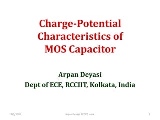
  • 1. Charge-Potential Characteristics of MOS Capacitor Arpan Deyasi Dept of ECE, RCCIIT, Kolkata, India 11/3/2020 1Arpan Deyasi, RCCIIT, India
  • 2. 11/3/2020 Arpan Deyasi, RCCIIT, India 2 VM>0 & large Al SiO2 Si(p) 1 2 point of inversion 3 ΨF ΨS RecapitulationofInversionCondition
  • 3. 11/3/2020 Arpan Deyasi, RCCIIT, India 3 VM>0 & large Al SiO2 Si(p) 1 2 point of inversion 3 ΨF ΨS ClassificationofInversion 2ΨF >Ψs>ΨF Weak inversion
  • 4. 11/3/2020 Arpan Deyasi, RCCIIT, India 4 VM>0 & large Al SiO2 Si(p) 1 2 point of inversion 3 ΨF ΨS ClassificationofInversion Ψs≥2ΨF Strong inversion
  • 5. Mathematical representation of band bending Band bending is defined Ψ(z) = ΨI(z) - ΨI(z ∞) Assumption Ψ(z)>0 for downward bending Ψ(z)<0 for downward bending Boundary conditions Ψ(z)=0 in bulk semiconductor Ψ(z=0) = ΨS at SiO2-Si interface 11/3/2020 5Arpan Deyasi, RCCIIT, India
  • 6. Poisson’s Equation for the Device [ ] 2 2 ( ) ( ) ( ) ( )D A d q p z n z N z N z dz ψ ε =− − + − In bulk substrate, p(z)=NA 2 ( ) i A n n z N = 11/3/2020 6Arpan Deyasi, RCCIIT, India
  • 7. Charge Neutrality Condition ( ) ( ) ( ) ( ) 0D Ap z n z N z N z− + − = ( ) 2 ( ) i D A A A n N z N z N N − = − 11/3/2020 7Arpan Deyasi, RCCIIT, India
  • 8. Charge Variation ( ) exp ( )i F I q p z n kT   = Ψ − Ψ   ( ) exp ( )i F q p z n kT   = Ψ − Ψ   11/3/2020 8Arpan Deyasi, RCCIIT, India
  • 9. Charge Variation ( ) exp expi F q q p z n kT kT     = Ψ −Ψ       ( ) expA q p z N kT   = −Ψ   11/3/2020 9Arpan Deyasi, RCCIIT, India
  • 10. Charge Variation ( ) exp ( )i I F q n z n kT   = Ψ − Ψ   ( ) exp ( )i F q n z n kT   = Ψ − Ψ   11/3/2020 10Arpan Deyasi, RCCIIT, India
  • 11. Charge Variation ( ) exp expi F q q n z n kT kT     = −Ψ Ψ       2 ( ) expi A n q n z N kT     = Ψ      11/3/2020 11Arpan Deyasi, RCCIIT, India
  • 12. Poisson’s Equation for the Device 2 2 22 exp exp A A i i A A q N N kTd q dz n nq N kT N ψ ε    −Ψ −    = −      − Ψ +         11/3/2020 12Arpan Deyasi, RCCIIT, India
  • 13. Poisson’s Equation for the Device 2 2 2 exp 1 exp 1 A i A q N kTd q dz n q N kT ψ ε     −Ψ −      = −     − Ψ −       11/3/2020 13Arpan Deyasi, RCCIIT, India
  • 14. Solution of Poisson’s Equation Step 2: Multiply both sides by (dΨ/dz) Step 1: Integrate from bulk (Ψ=0) to surface [(dΨ/dz)=0] 11/3/2020 14Arpan Deyasi, RCCIIT, India
  • 15. Solution of Poisson’s Equation 2 2 2 0 0 exp 1 exp 1 d Adz i A q N kTd q dz n q N kT ψ ε Ψ Ψ     −Ψ −      = −     − Ψ −       ∫ ∫ 11/3/2020 15Arpan Deyasi, RCCIIT, India
  • 16. 11/3/2020 Arpan Deyasi, RCCIIT, India 16 0 2 0 exp 1 exp 1 d dz A i A d d q dz dz q N kT n q N kT ψ ε Ψ Ψ   =− ×        −Ψ −           − Ψ −       ∫ ∫ Solution of Poisson’s Equation
  • 17. Solution of Poisson’s Equation 0 2 0 exp 1 exp 1 d dz d Adz i A d d d dz dz dz q N kTq d dzn q N kT ψ ψ ψ ε Ψ Ψ     × =            −Ψ −        − ×       − Ψ −       ∫ ∫ 11/3/2020 17Arpan Deyasi, RCCIIT, India
  • 18. Solution of Poisson’s Equation 0 2 0 exp 1 exp 1 d dz A i A d d d dz dz q N kTq d n q N kT ψ ψ ψ ε Ψ Ψ     =            −Ψ −      − ×     − Ψ −       ∫ ∫ 11/3/2020 18Arpan Deyasi, RCCIIT, India
  • 19. Expression of Electric Field [ ] 2 2 2 2 2 ( ) exp 1 exp 1 A i A d kTN z dz q q kT kT n q q kT kTN ψ ξ ε   = = ×      Ψ Ψ     − + −              Ψ Ψ      + − −            11/3/2020 19Arpan Deyasi, RCCIIT, India
  • 20. 11/3/2020 20Arpan Deyasi, RCCIIT, India Boundary condition for Electric Field at z=0 (insulator-semiconductor interface) [i] Ψ = ΨS [ii] ξ = ξS
  • 21. 11/3/2020 Arpan Deyasi, RCCIIT, India 21 Surface Electric Field 0.5 2 2 2 exp 1 exp 1 A S S S i S S A kTN q q kT kT n q q kT kTN ξ ε = ×   Ψ Ψ     − + −              Ψ Ψ      + − −           
  • 22. 11/3/2020 Arpan Deyasi, RCCIIT, India 22 Surface Charge From Gauss’ law S SQ εξ= − 0.5 2 2 2 exp 1 exp 1 S S A S S i S S A Q kTN q q kT kT n q q kT kTN εξ ε=− = ×   Ψ Ψ     − + −              Ψ Ψ      + − −           
  • 23. 11/3/2020 Arpan Deyasi, RCCIIT, India 23 Graphical representation of Charge Profile CASE-I 0 0 S SQ Ψ = = at flat-band condition ΨS QS
  • 24. 11/3/2020 Arpan Deyasi, RCCIIT, India 24 Graphical representation of Charge Profile CASE-II 0SΨ < accumulation condition exp 2 S S q Q kT Ψ  ∝ −    ΨS QS
  • 25. 11/3/2020 Arpan Deyasi, RCCIIT, India 25 Graphical representation of Charge Profile CASE-III depletion condition 0&S smallΨ > 1/2 S SQ ∝ Ψ ΨS QS
  • 26. 11/3/2020 Arpan Deyasi, RCCIIT, India 26 Graphical representation of Charge Profile CASE-IV inversion condition ΨS QS 0&SΨ > large exp 2 S S q Q kT Ψ  ∝    
  • 27. 11/3/2020 Arpan Deyasi, RCCIIT, India 27 ΨS QS Graphical representation of Charge Profile accumulation depletion weak inversion strong inversion ΨF ΨF Distance from flat-band point to point of inversion is ΨF Distance from point of inversion to inversion transition is also ΨF