SPICE MODEL of TPCA8015-H (Standard+BDS Model) in SPICE PARK
•
0 likes•255 views

SPICE MODEL of TPCA8015-H (Standard+BDS) in SPICE PARK. English Version is http://www.spicepark.net. Japanese Version is http://www.spicepark.com by Bee Technologies.

Recommended
Recommended
More Related Content
What's hot
What's hot (20)
Viewers also liked
Viewers also liked (7)
Similar to SPICE MODEL of TPCA8015-H (Standard+BDS Model) in SPICE PARK
Similar to SPICE MODEL of TPCA8015-H (Standard+BDS Model) in SPICE PARK (20)
More from Tsuyoshi Horigome
More from Tsuyoshi Horigome (20)
Recently uploaded
Recently uploaded (20)
SPICE MODEL of TPCA8015-H (Standard+BDS Model) in SPICE PARK
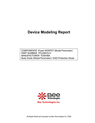
- 1. Device Modeling Report COMPONENTS: Power MOSFET (Model Parameter) PART NUMBER: TPCA8015-H MANUFACTURER: TOSHIBA Body Diode (Model Parameter) / ESD Protection Diode Bee Technologies Inc. All Rights Reserved Copyright (c) Bee Technologies Inc. 2006
- 2. MOSFET MODEL Pspice model Model description parameter LEVEL L Channel Length W Channel Width KP Transconductance RS Source Ohmic Resistance RD Ohmic Drain Resistance VTO Zero-bias Threshold Voltage RDS Drain-Source Shunt Resistance TOX Gate Oxide Thickness CGSO Zero-bias Gate-Source Capacitance CGDO Zero-bias Gate-Drain Capacitance CBD Zero-bias Bulk-Drain Junction Capacitance MJ Bulk Junction Grading Coefficient PB Bulk Junction Potential FC Bulk Junction Forward-bias Capacitance Coefficient RG Gate Ohmic Resistance IS Bulk Junction Saturation Current N Bulk Junction Emission Coefficient RB Bulk Series Resistance PHI Surface Inversion Potential GAMMA Body-effect Parameter DELTA Width effect on Threshold Voltage ETA Static Feedback on Threshold Voltage THETA Modility Modulation KAPPA Saturation Field Factor VMAX Maximum Drift Velocity of Carriers XJ Metallurgical Junction Depth UO Surface Mobility All Rights Reserved Copyright (c) Bee Technologies Inc. 2006
- 3. Transconductance Characteristic Circuit Simulation Result Comparison table gfs Id(A) Error(%) Measurement Simulation 1.000 23.000 23.274 1.191 2.000 30.000 31.004 3.347 5.000 45.000 45.471 1.047 10.00 60.000 59.683 -0.528 All Rights Reserved Copyright (c) Bee Technologies Inc. 2006
- 4. Vgs-Id Characteristic Circuit Simulation result 100A 80A 60A 40A 20A 0A 0V 1.0V 2.0V 3.0V 4.0V 5.0V 6.0V I(V3) V_V1 Evaluation circuit TPCA8015-H U2 V3 0Vdc V2 10Vdc V1 10Vdc 0 All Rights Reserved Copyright (c) Bee Technologies Inc. 2006
- 5. Comparison Graph Circuit Simulation Result Simulation Result VGS(V) ID(A) Error (%) Measurement Simulation 2.000 2.600 2.702 3.919 5.000 2.690 2.781 3.398 10.000 2.810 2.878 2.406 20.000 2.970 3.026 1.872 50.000 3.300 3.361 1.839 100.000 3.800 3.804 0.116 All Rights Reserved Copyright (c) Bee Technologies Inc. 2006
- 6. Rds(on) Characteristic Circuit Simulation result 17.5A 15.0A 12.5A 10.0A 7.5A 5.0A 2.5A 0A 0V 200mV 400mV 500mV I(V3) V_V2 Evaluation circuit TPCA8015-H U2 V3 0Vdc V2 10Vdc V1 10Vdc 0 Simulation Result ID=17.5A, VGS=10V Measurement Simulation Error (%) R DS (on) 4.400 m 4.460 m 1.364 All Rights Reserved Copyright (c) Bee Technologies Inc. 2006
- 7. Gate Charge Characteristic Circuit Simulation result 16V 12V 8V 4V 0V 0s 10ns 20ns 30ns 40ns V(U2:4) Time*1m Evaluation circuit TPCA8015-H U2 V2 0Vdc W1 + - W D1 IOFF = 10m Dbreak I2 PER = 1000u ION = 0uA DC = 35Adc PW = 600u ROFF = 100G TF = 10n RON = 1m TR = 10n TD = 0 I2 = 10m V1 I1 32Vdc I1 = 0 0 Simulation Result VDD=32V,ID= 35A Measurement Simulation Error (%) ,VGS=5V Qgs 7.000 nC 7.288 nC 4.114 Qgd 9.000 nC 8.640 nC 4.000 All Rights Reserved Copyright (c) Bee Technologies Inc. 2006
- 8. Capacitance Characteristic Measurement Simulation Simulation Result Cbd(pF) VDS(V) Error(%) Measurement Simulation 0.100 2120.000 2100.000 -0.943 0.200 2060.000 2000.000 -2.913 0.500 1750.000 1760.000 0.571 1.000 1500.000 1500.000 0.000 2.000 1200.000 1250.000 4.167 5.000 780.000 790.000 1.282 10.000 550.000 560.000 1.818 20.000 400.000 405.000 1.250 40.000 290.000 280.000 -3.448 All Rights Reserved Copyright (c) Bee Technologies Inc. 2006
- 9. Switching Time Characteristic Circuit Simulation result 12V 11V 10V 9V 8V 7V 6V 5V 4V 3V 2V 1V 0V 4.962us 4.980us 5.000us 5.020us 5.040us 5.060us V(2) V(3)/2 Time Evaluation circuit TPCA8015-H U2 R3 L1 L2 2 3 4.7 30nH 50nH V3 RL V1 = 0 0Vdc R4 1.11 V1 V2 = 20 VDD TD = 5u 4.7 TR = 6n 20 TF = 6n PW = 5u PER = 10u 0 0 0 0 Simulation Result ID=17.5A, VDD= 20V Measurement Simulation Error(%) VGS=0/10V ton 12.000 ns 12.029 ns 0.242 All Rights Reserved Copyright (c) Bee Technologies Inc. 2006
- 10. Output Characteristic Circuit Simulation result 100A 3.8 V 10 3.7 V 4 6 80A 4.5 3.5 V 60A 3.4 V 3.2 V 40A 3.0V 20A VGS= 2.8V 0A 0V 1.0V 2.0V 3.0V 4.0V 5.0V I(V3) V_V2 Evaluation circuit TPCA8015-H U2 V3 0Vdc V2 10Vdc V1 10Vdc 0 All Rights Reserved Copyright (c) Bee Technologies Inc. 2006
- 11. BODY DIODE SPICE MODEL Forward Current Characteristic Circuit Simulation Result 100A 10A 1.0A 100mA 0V 0.2V 0.4V 0.6V 0.8V 1.0V I(R1) V_V1 Evaluation Circuit R1 0.01m U2 TPCA8015-H V1 0Vdc 0 All Rights Reserved Copyright (c) Bee Technologies Inc. 2006
- 12. Comparison Graph Circuit Simulation Result Simulation Result VSD(V) IDR(A) %Error Measurement Simulation 0.100 0.590 0.587 -0.508 0.200 0.605 0.604 -0.165 0.500 0.627 0.627 0.000 1.000 0.645 0.646 0.155 2.000 0.665 0.666 0.150 5.000 0.700 0.697 -0.429 10.000 0.730 0.727 -0.411 20.000 0.770 0.765 -0.649 50.000 0.830 0.830 0.000 100.000 0.900 0.900 0.000 All Rights Reserved Copyright (c) Bee Technologies Inc. 2006
- 13. Reverse Recovery Characteristic Circuit Simulation Result 400mA 300mA 200mA 100mA -0mA -100mA -200mA -300mA -400mA 0.7us 0.9us 1.1us 1.3us 1.5us 1.7us I(R1) Time Evaluation Circuit R1 50 V1 = -9.4V V2 = 10.6V TD = 60n V1 TR = 12n TF = 10n TPCA8015-H PW = 1u PER = 2u 0 Compare Measurement vs. Simulation Measurement Simulation Error (%) trj 18.000 ns 17.934 ns -0.367 trb 112.000 ns 110.345 ns -1.478 trr 130.000 ns 128.279 ns -1.324 All Rights Reserved Copyright (c) Bee Technologies Inc. 2006
- 14. Reverse Recovery Characteristic Reference Trj=18 (ns) Trb=112(ns) Conditions:Ifwd=lrev=0.2(A),Rl=50 Example Relation between trj and trb All Rights Reserved Copyright (c) Bee Technologies Inc. 2006
- 15. ESD PROTECTION DIODE SPICE MODEL Zener Voltage Characteristic Circuit Simulation Result 10mA 9mA 8mA 7mA 6mA 5mA 4mA 3mA 2mA 1mA 0A 0V 5V 10V 15V 20V 25V 30V 35V 40V 45V 50V I(R1) V_V1 Evaluation Circuit R1 U7 0.01m V1 0Vdc TPCA8015_H Ropen 100MEG 0 All Rights Reserved Copyright (c) Bee Technologies Inc. 2006
- 16. Zener Voltage Characteristic Reference All Rights Reserved Copyright (c) Bee Technologies Inc. 2006