Download to read offline
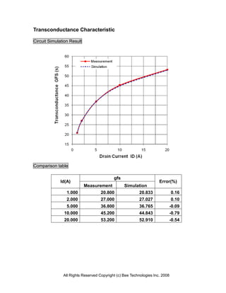
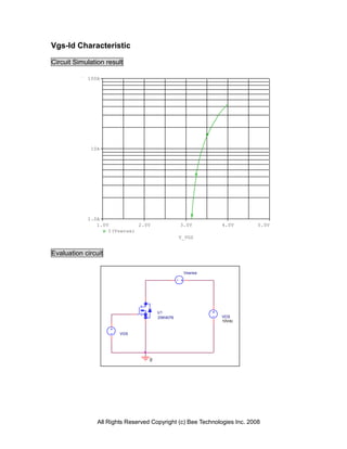
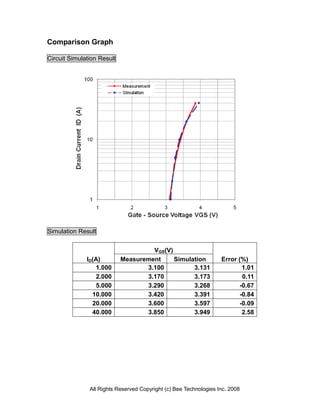
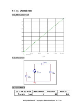
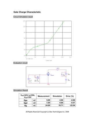
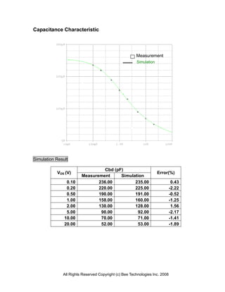
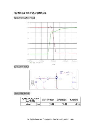
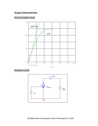
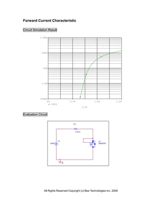
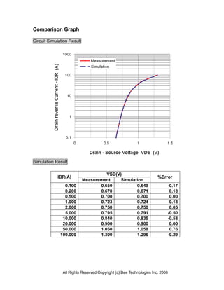
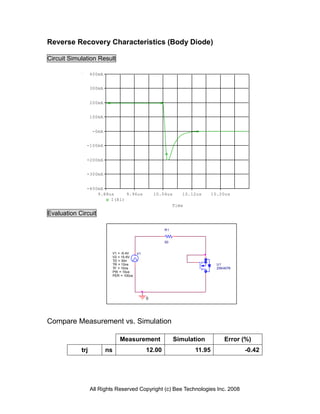
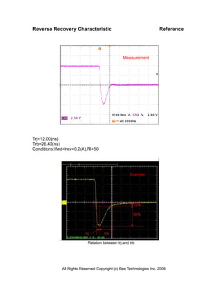

The document presents a detailed power MOSFET modeling report for the part number 2SK4076 manufactured by NEC, including model parameters, circuit simulation results, and characteristic curves. It covers transconductance, gate charge, capacitance, switching time, and reverse recovery characteristics, all with associated error percentages from measurements and simulations. The findings aim to provide essential insights for engineers working with this specific MOSFET in circuit applications.


