Device Modeling Report for Power MOSFET
•
0 likes•208 views

This document summarizes the key parameters and simulation results of a power MOSFET transistor and its internal body diode. It includes tables of parameters for the MOSFET and diode models, graphs comparing simulated and measured output characteristics like forward current and switching times, and evaluation circuits used in the simulations. The models aim to accurately represent the electrical behavior of the real components for circuit design and analysis.

Recommended
Recommended
More Related Content
What's hot
What's hot (20)
Similar to Device Modeling Report for Power MOSFET
Similar to Device Modeling Report for Power MOSFET (13)
More from Tsuyoshi Horigome
More from Tsuyoshi Horigome (20)
Recently uploaded
Recently uploaded (20)
Device Modeling Report for Power MOSFET
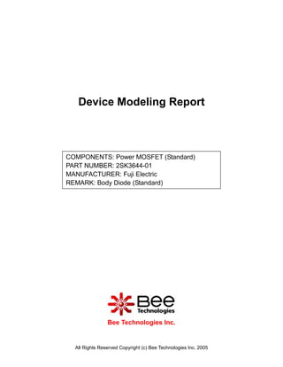
- 1. Device Modeling Report COMPONENTS: Power MOSFET (Standard) PART NUMBER: 2SK3644-01 MANUFACTURER: Fuji Electric REMARK: Body Diode (Standard) Bee Technologies Inc. All Rights Reserved Copyright (c) Bee Technologies Inc. 2005
- 2. POWER MOSFET MODEL Pspice model Model description parameter LEVEL L Channel Length W Channel Width KP Transconductance RS Source Ohmic Resistance RD Ohmic Drain Resistance VTO Zero-bias Threshold Voltage RDS Drain-Source Shunt Resistance TOX Gate Oxide Thickness CGSO Zero-bias Gate-Source Capacitance CGDO Zero-bias Gate-Drain Capacitance CBD Zero-bias Bulk-Drain Junction Capacitance MJ Bulk Junction Grading Coefficient PB Bulk Junction Potential FC Bulk Junction Forward-bias Capacitance Coefficient RG Gate Ohmic Resistance IS Bulk Junction Saturation Current N Bulk Junction Emission Coefficient RB Bulk Series Resistance PHI Surface Inversion Potential GAMMA Body-effect Parameter DELTA Width effect on Threshold Voltage ETA Static Feedback on Threshold Voltage THETA Modility Modulation KAPPA Saturation Field Factor VMAX Maximum Drift Velocity of Carriers XJ Metallurgical Junction Depth UO Surface Mobility All Rights Reserved Copyright (c) Bee Technologies Inc. 2005
- 3. Body Diode Model Pspice model Model description parameter IS Saturation Current N Emission Coefficient RS Series Resistance IKF High-injection Knee Current CJO Zero-bias Junction Capacitance M Junction Grading Coefficient VJ Junction Potential ISR Recombination Current Saturation Value BV Reverse Breakdown Voltage(a positive value) IBV Reverse Breakdown Current(a positive value) TT Transit Time All Rights Reserved Copyright (c) Bee Technologies Inc. 2005
- 4. Transconductance Characteristic Circuit Simulation Result Comparison table VGS(V) ID(A) Error (%) Measurement Simulation 1.000 5.000 4.965 -0.700 2.000 7.000 6.775 -3.214 5.000 10.500 10.470 -0.286 10.000 14.300 14.180 -0.839 20.000 19.000 18.940 -0.316 All Rights Reserved Copyright (c) Bee Technologies Inc. 2005
- 5. Vgs-Id Characteristic Circuit Simulation result 100A 10A 1.0A 500mA 0V 5V 10V I(V2) V_V1 Evaluation circuit V2 0V dc V3 V1 10 Vd c 25 Vd c 0 All Rights Reserved Copyright (c) Bee Technologies Inc. 2005
- 6. Comparison Graph Circuit Simulation Result Simulation Result VGS(V) ID(A) Error (%) Measurement Simulation 1.000 5.350 5.350 -0.002 2.000 5.550 5.519 -0.568 5.000 5.900 5.863 -0.627 10.000 6.300 6.269 -0.494 All Rights Reserved Copyright (c) Bee Technologies Inc. 2005
- 7. Id-Rds(on) Characteristic Circuit Simulation result 15A 10A 5A 0A 0V 1.0V 2.0V I(V2) V_V3 Evaluation circuit V2 0Vdc V3 V1 10Vdc 25Vdc 0 Simulation Result ID=15, VGS=10V Measurement Simulation Error (%) R DS (on) 34.000 m 34.067 m 0.197 All Rights Reserved Copyright (c) Bee Technologies Inc. 2005
- 8. Gate Charge Characteristic Circuit Simulation result 14V 12V 10V 8V 6V 4V 2V 0V 0 10n 20n 30n 40n 50n V(W1:3) Time*10ms Evaluation circuit V2 0Vdc Dbreak PER = 1000u D1 PW = 600u I2 TF = 10n W1 30Adc TR = 10n + TD = 0 I2 = 10m - I1 W I1 = 0 IOFF = 1mA V1 ION = 0uA 50Vdc 0 Simulation Result VDD=50V Measurement Simulation Error (%) ,ID=30A Qgs 13.000 nC 12.975 nC 0.192 Qgd 9.000 nC 8.926 nC 0.827 All Rights Reserved Copyright (c) Bee Technologies Inc. 2005
- 9. Capacitance Characteristic (Vds vs. Cbd) Measurement Simulation Simulation Result Cbd(pF) VDS(V) Error(%) Measurement Simulation 1.000 1.750 1.759 0.514 2.000 1.430 1.429 -0.070 5.000 1.000 1.013 1.250 10.000 0.770 0.750 -2.597 20.000 0.580 0.550 -5.172 50.000 0.350 0.352 0.571 All Rights Reserved Copyright (c) Bee Technologies Inc. 2005
- 10. Switching Time Characteristic Circuit Simulation result 12.0V VDS =48 (V) VGS = 10V 8.0V 4.0V 0V 5.000us 5.050us 5.100us V(2) V(3)/4.8 Time Evaluation circuit L1 RL 3 V3 0.05uH 3.175 0Vdc VDD 48 L2 RG 2 0.03uH 10 V1 = 0 0 V1 V2 = 10 TD = 5u TR = 6n TF = 7n PW = 10u PER = 100u 0 0 Simulation Result ID=15A, VDD=48V Measurement Simulation Error(%) VGS=0/10V td (on) 16.000 ns 16.063 ns 0.394 All Rights Reserved Copyright (c) Bee Technologies Inc. 2005
- 11. Output Characteristic Circuit Simulation result 10A 6.5V 6.0V 5A VGS=5.5V 0A 0V 25V 50V I(V2) V_V3 Evaluation circuit V2 0V dc V3 V1 25 Vd c 10 .0Vd c 0 All Rights Reserved Copyright (c) Bee Technologies Inc. 2005
- 12. Output Characteristic Reference 6.5V 6.0V VGS=5.5V All Rights Reserved Copyright (c) Bee Technologies Inc. 2005
- 13. Forward Current Characteristic of Reverse Diode Circuit Simulation Result 40A 10A 1.0A 100mA 0V 1.0V 2.0V I(V2) V_V3 Evaluation Circuit R1 0.0 1m V2 0V dc V3 0V dc 0 All Rights Reserved Copyright (c) Bee Technologies Inc. 2005
- 14. Comparison Graph Circuit Simulation Result Simulation Result Vfwd(V) Vfwd(V) Ifwd(A) %Error Measurement Simulation 0.100 0.620 0.621 0.081 0.200 0.648 0.647 -0.154 0.500 0.678 0.676 -0.295 1.000 0.702 0.699 -0.499 2.000 0.724 0.721 -0.483 5.000 0.746 0.750 0.536 10.000 0.770 0.772 0.260 All Rights Reserved Copyright (c) Bee Technologies Inc. 2005
- 15. Reverse Recovery Characteristic Circuit Simulation Result 400mA 0A -400mA 4.4us 4.8us 5.2us 5.6us 6.0us 6.4us I(R1) Time Evaluation Circuit R1 50 U9 2SK3644-01S V1 = {-9.4} V1 V2 = {10.7} TD = 100n TR = 10n TF = 10n PW = 5u PER = 50u 0 0 Compare Measurement vs. Simulation Measurement Simulation Error (%) trr=trj+trb 284.000 ns 284.527 ns 0.186 All Rights Reserved Copyright (c) Bee Technologies Inc. 2005
- 16. Reverse Recovery Characteristic Reference Trj=142(ns) Trb=142(ns) Conditions:Ifwd=lrev=0.2(A),Rl=50 Example Relation between trj and trb All Rights Reserved Copyright (c) Bee Technologies Inc. 2005