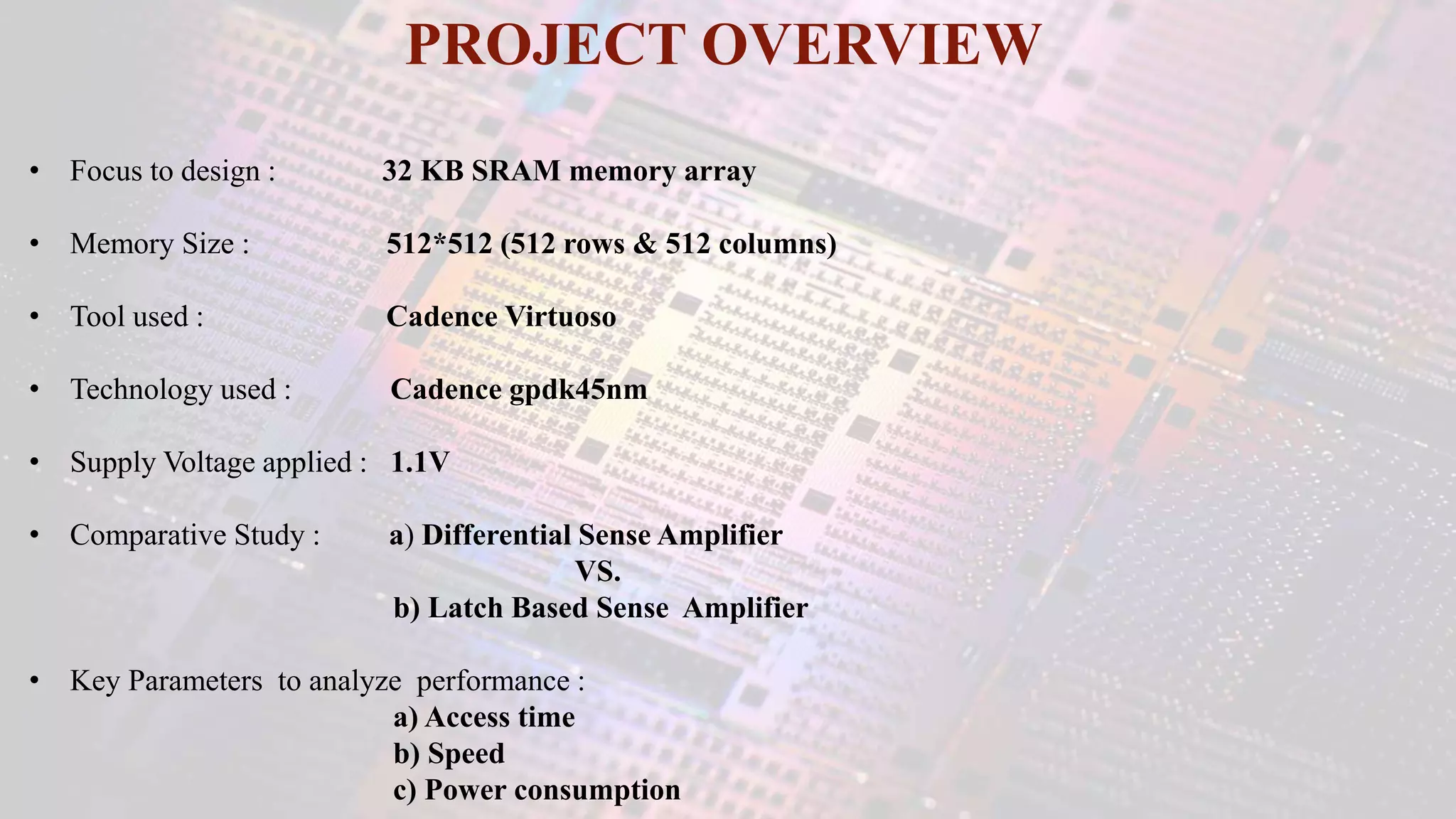
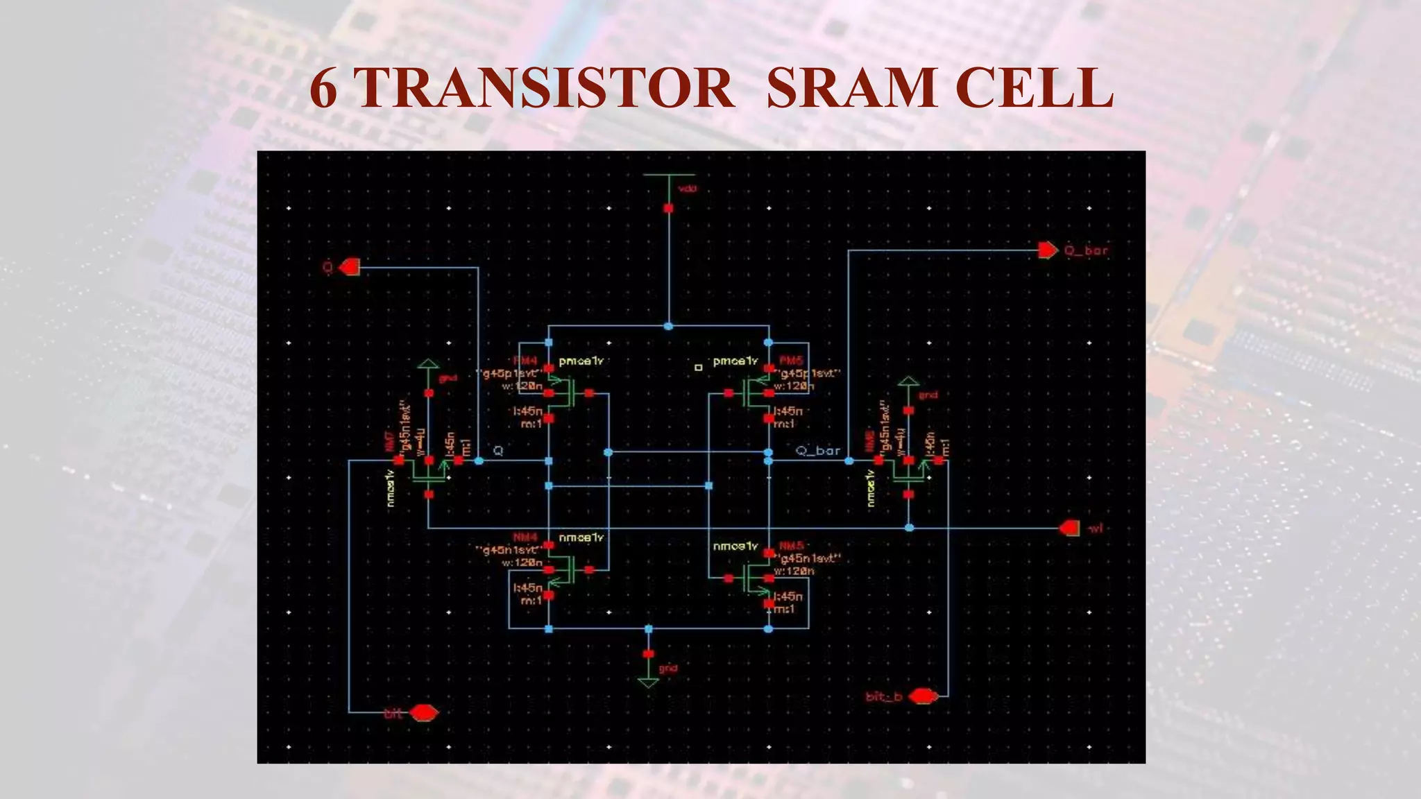
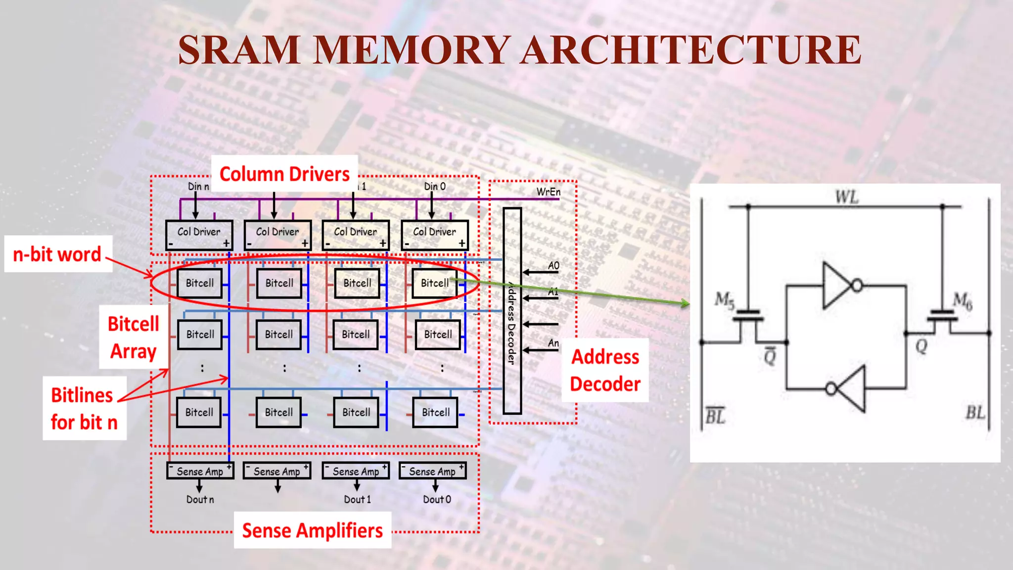
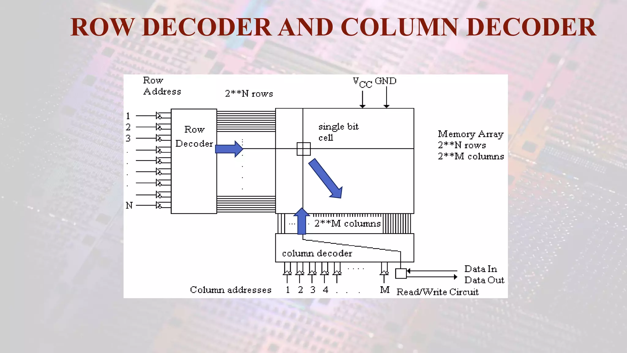
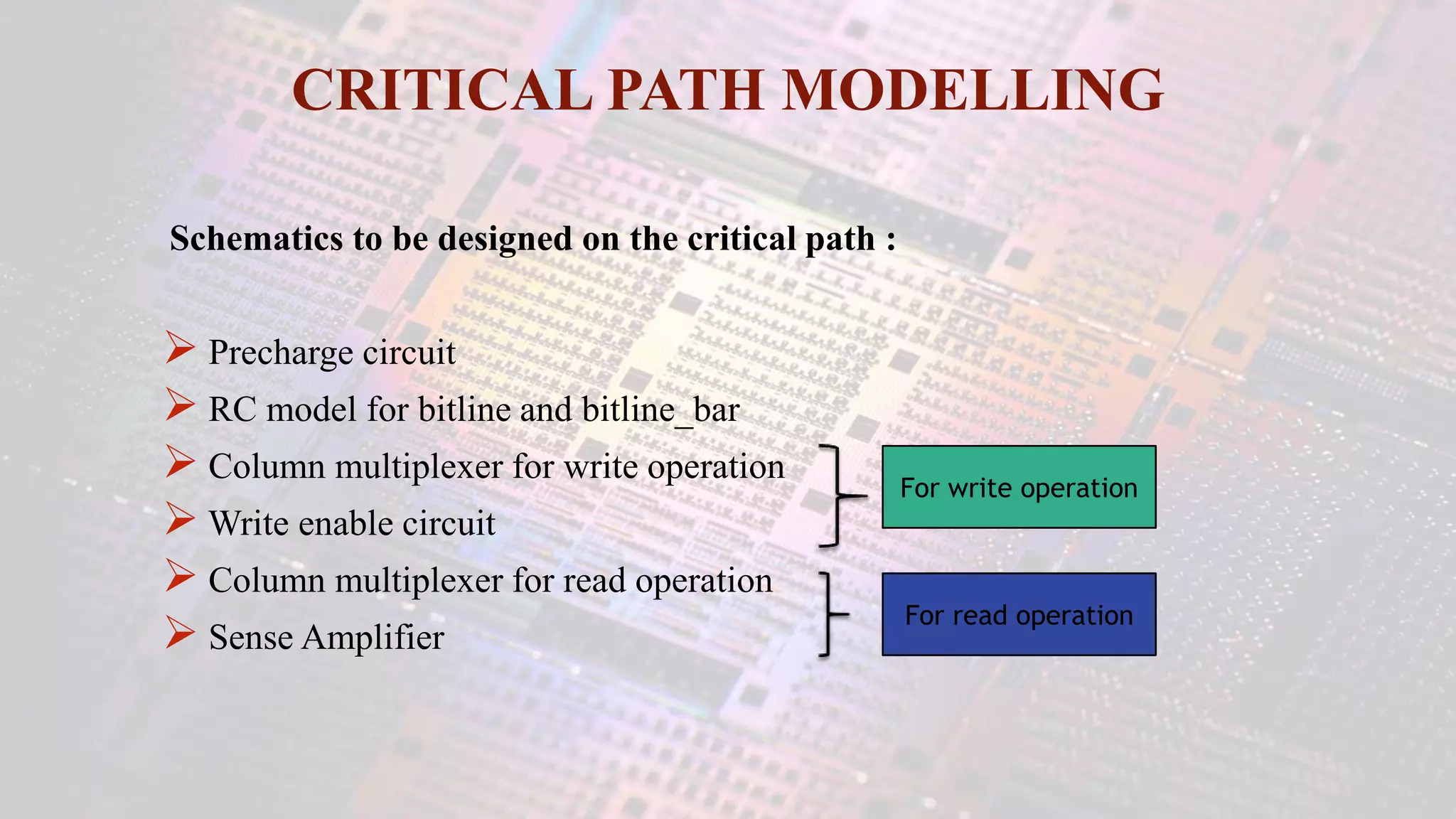
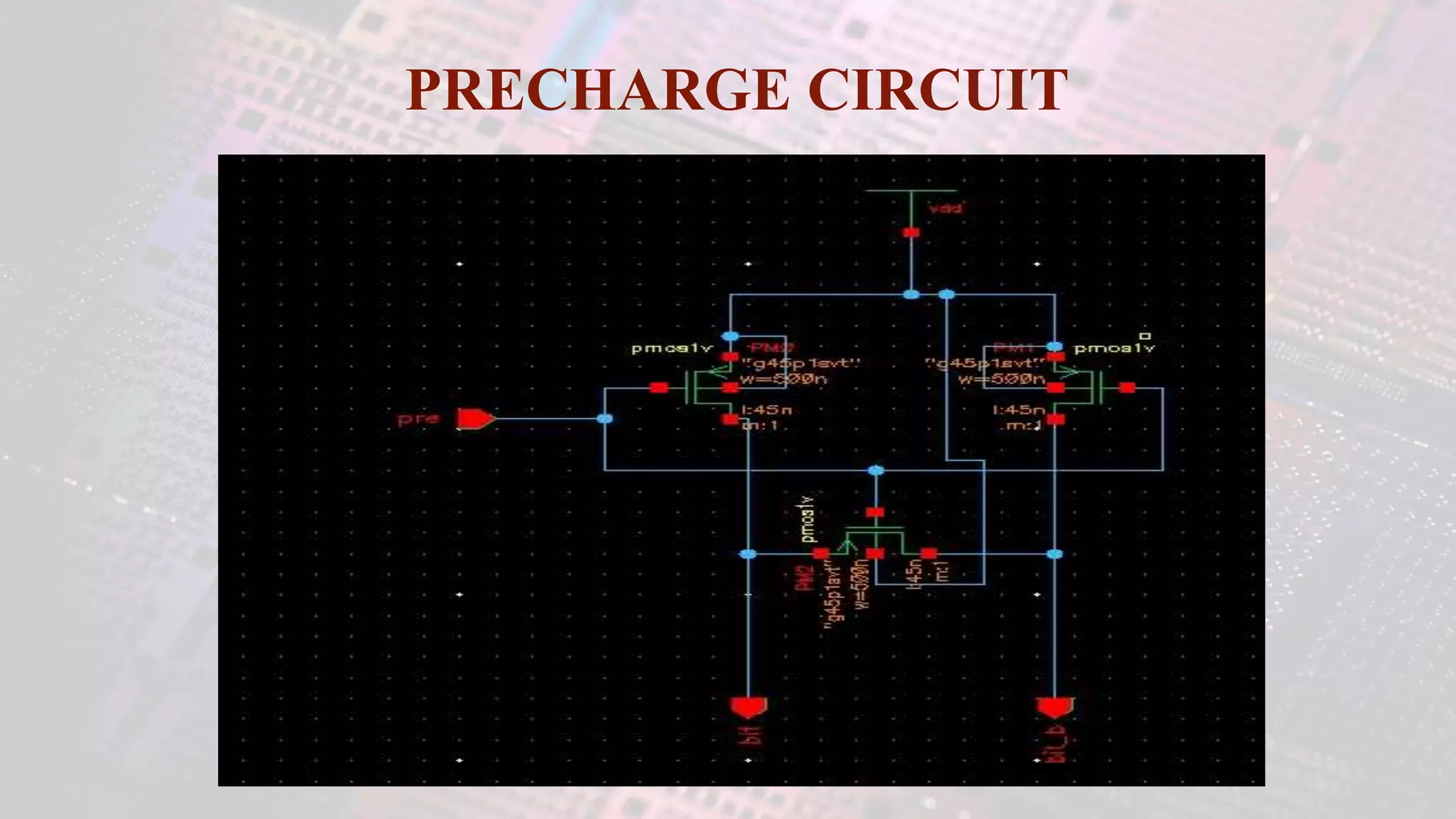
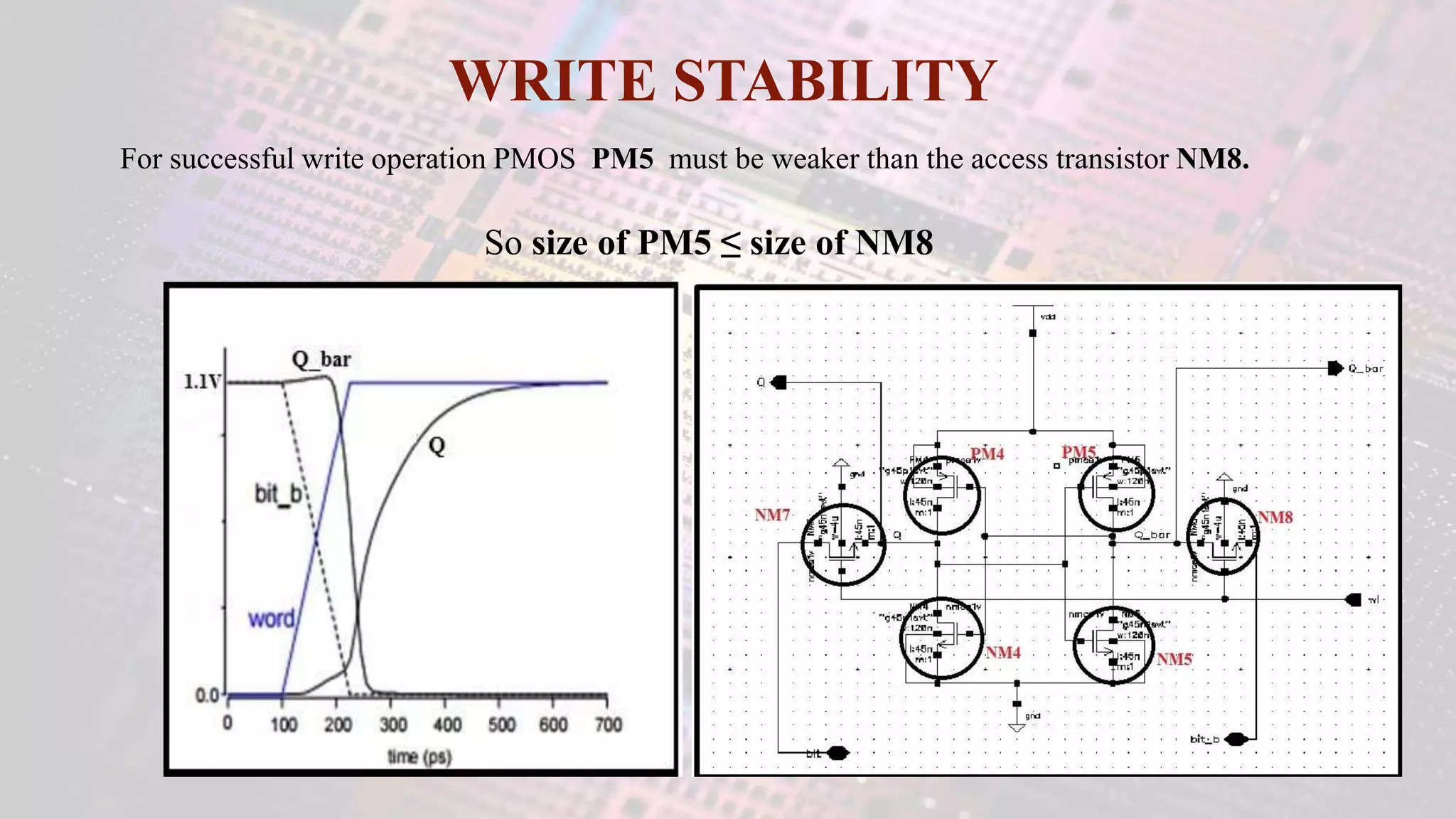
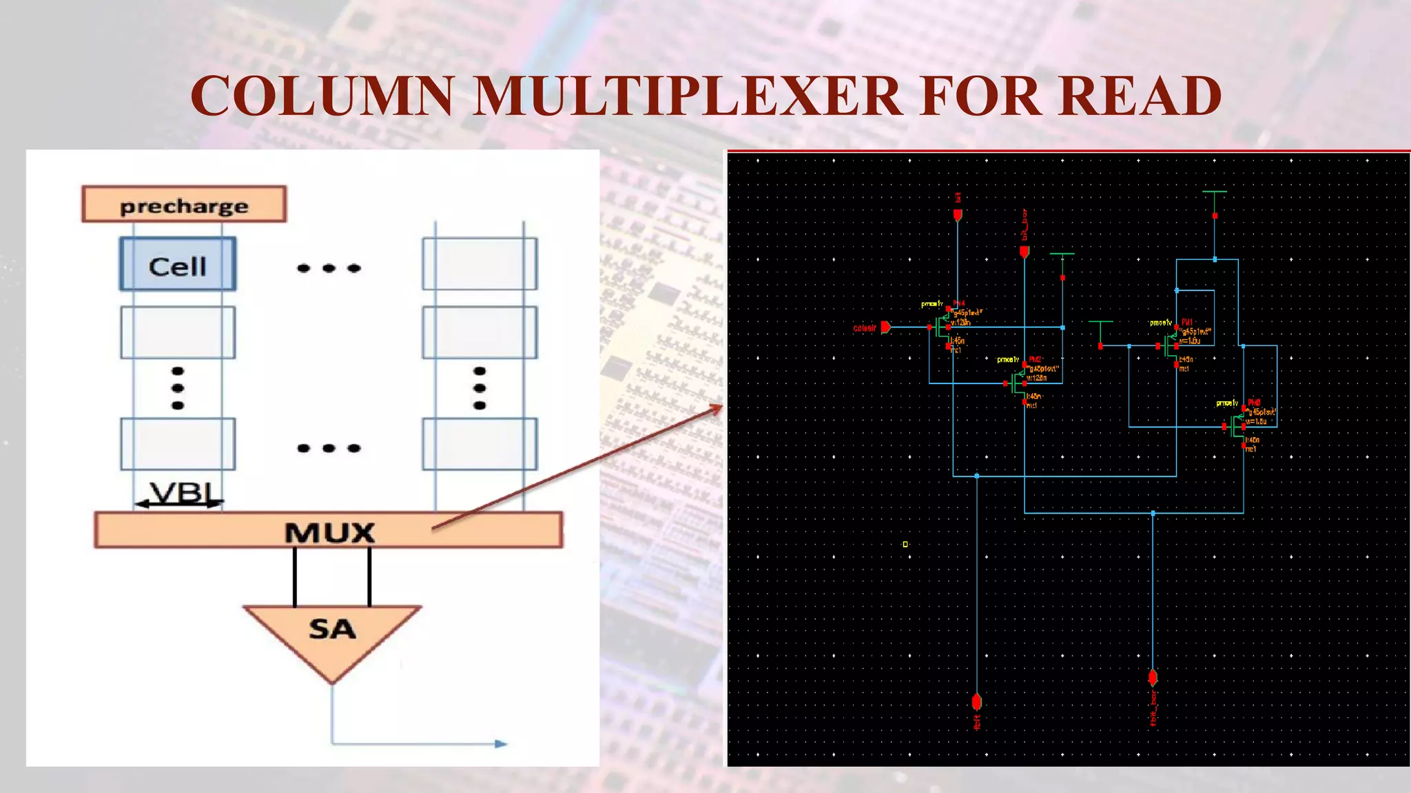
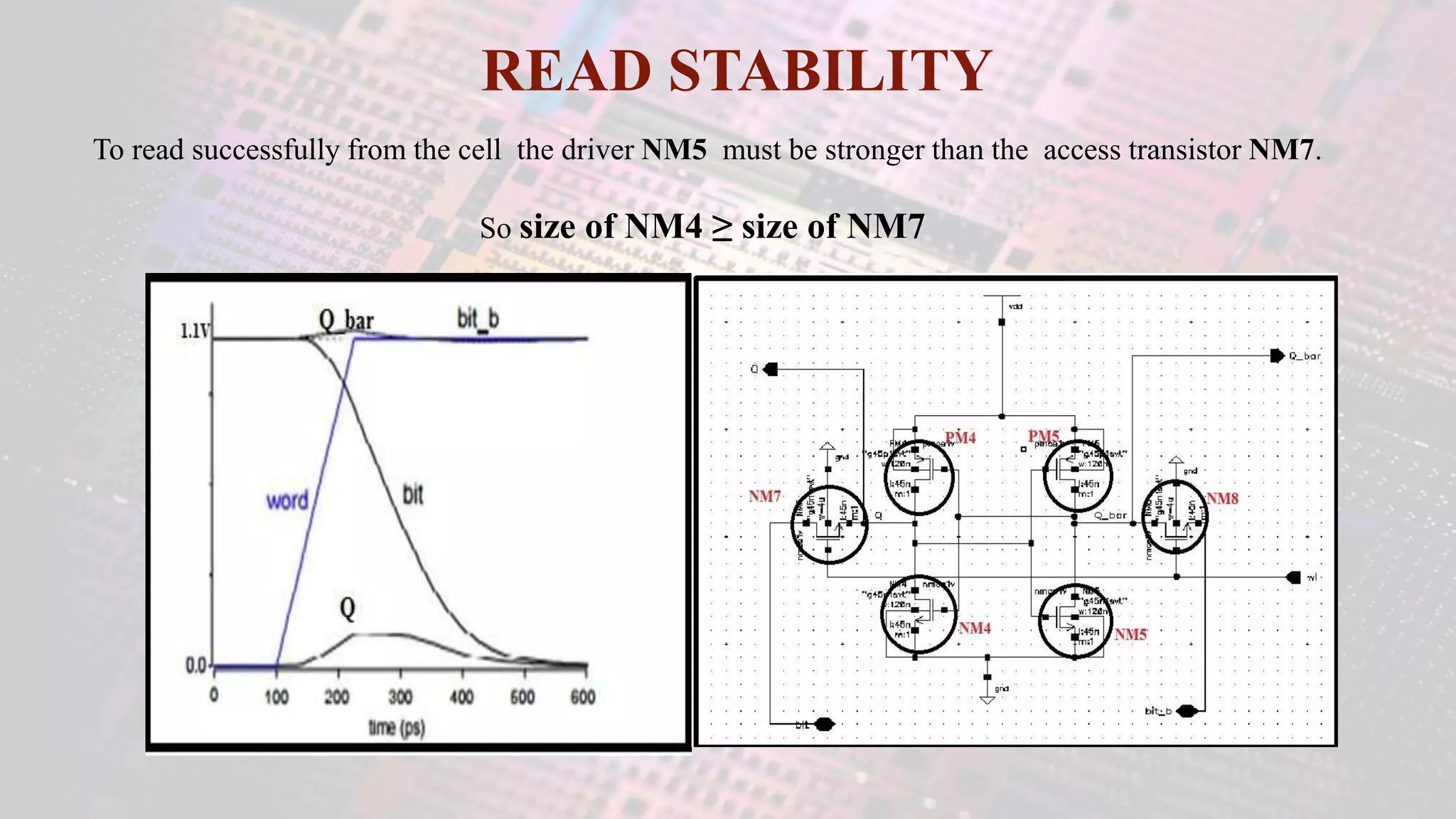
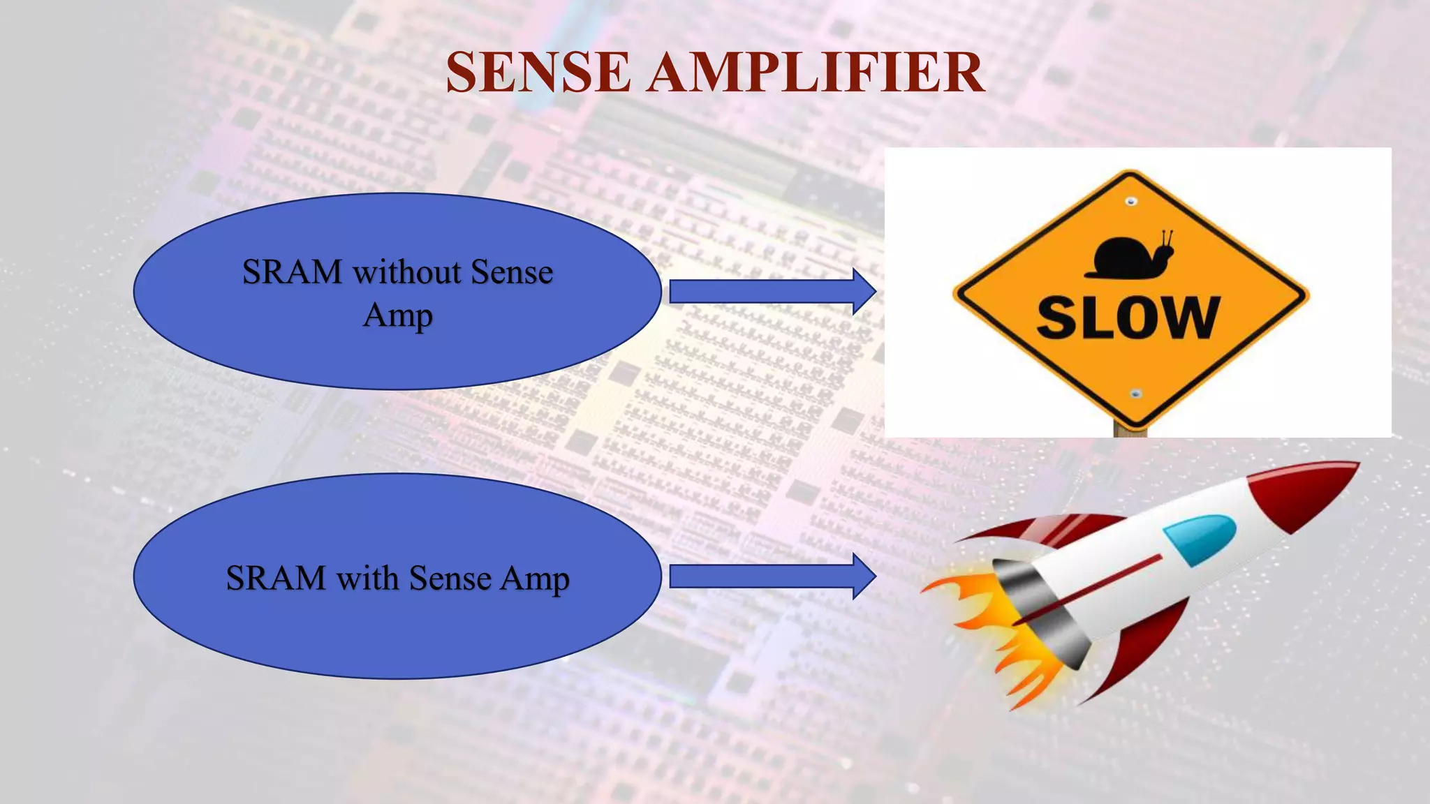
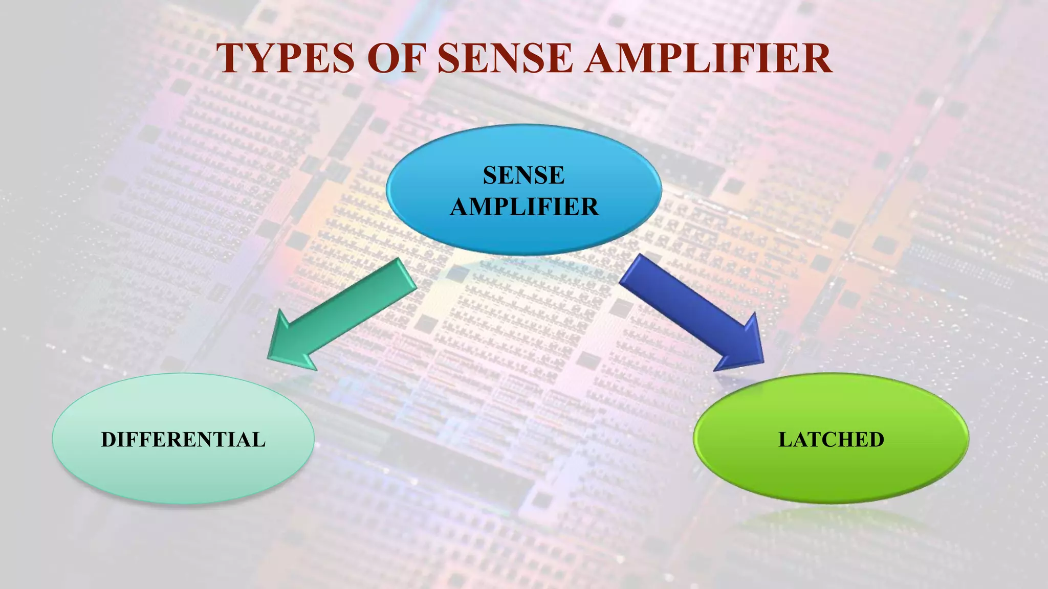
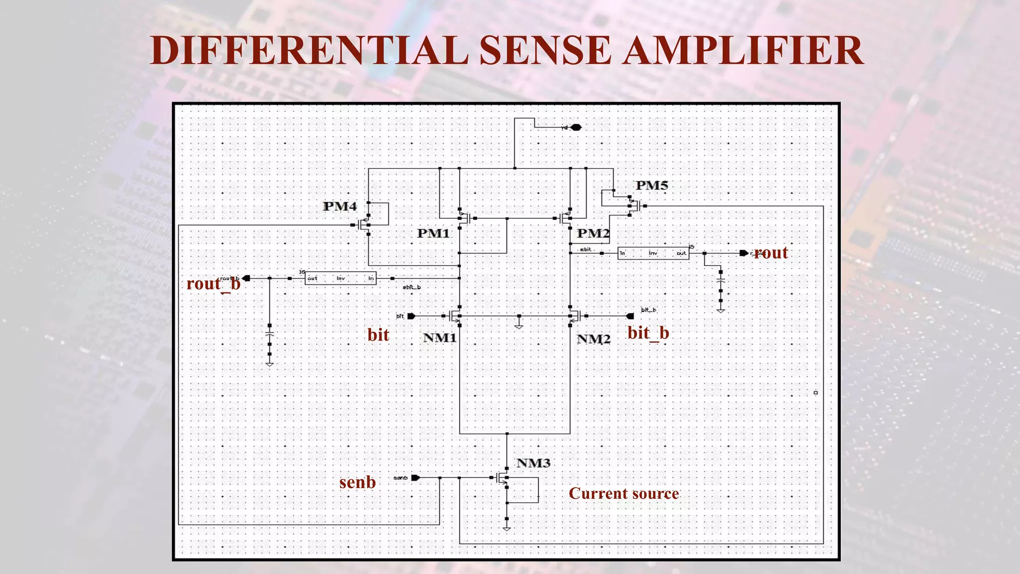
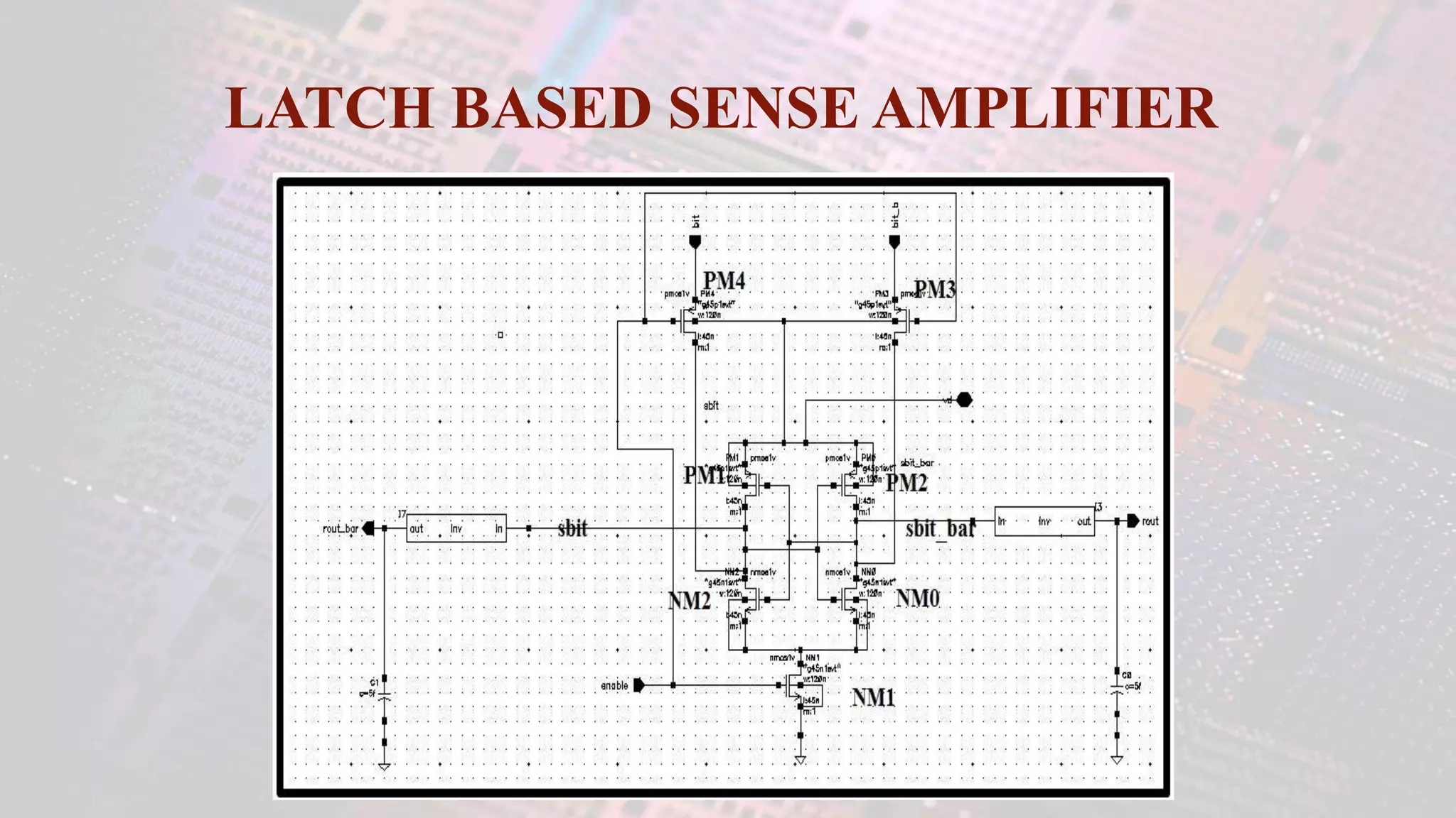
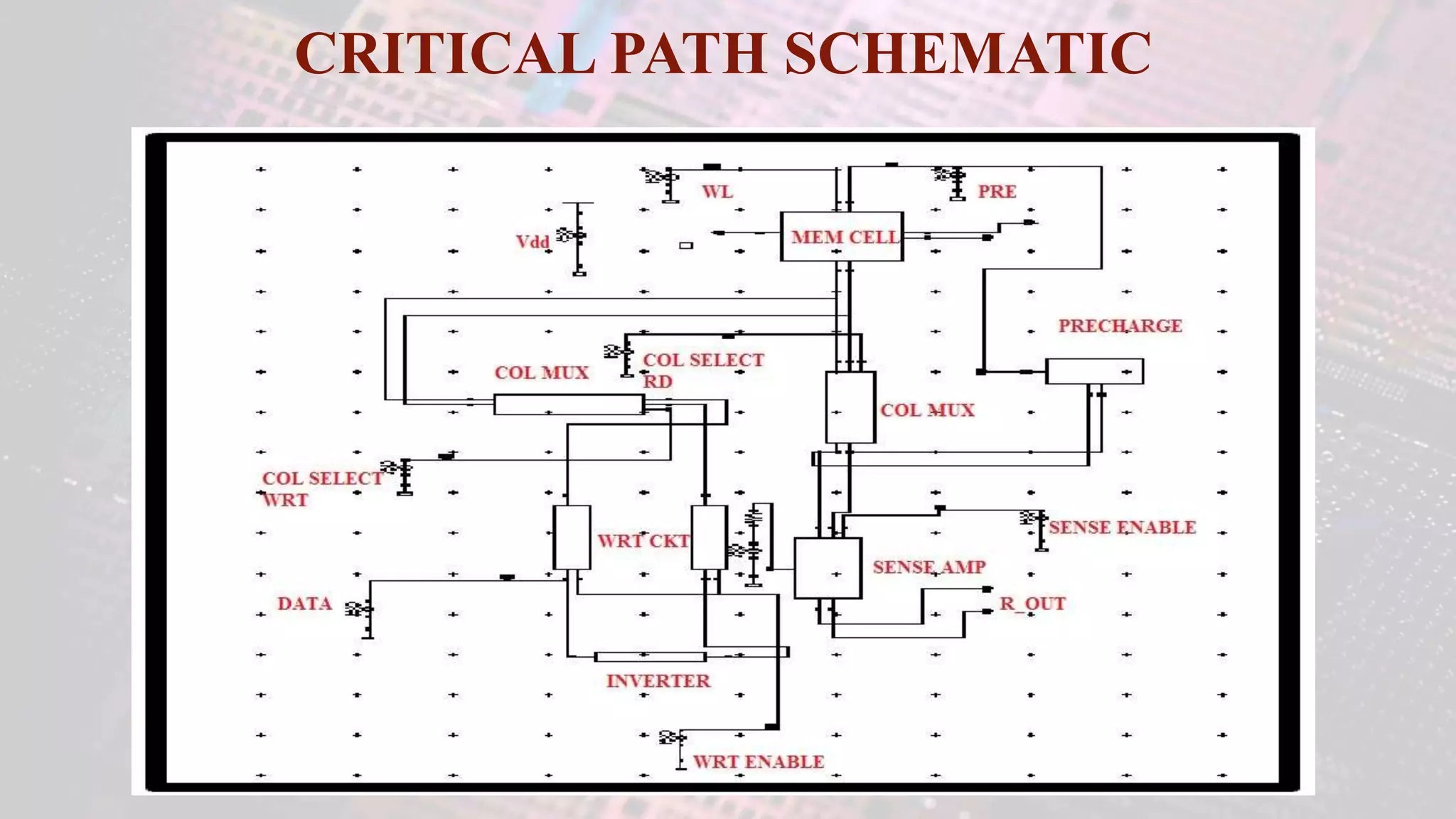
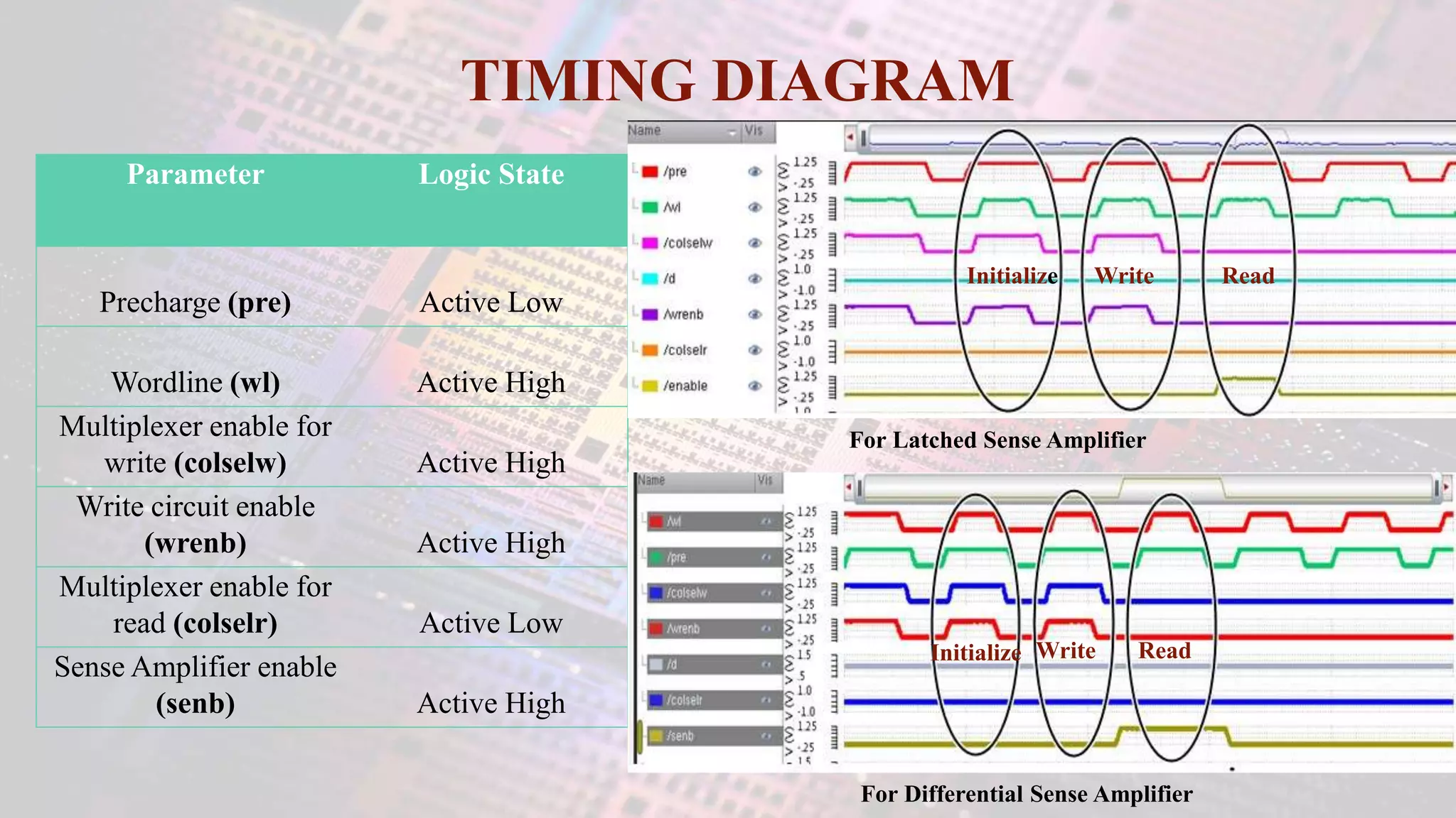
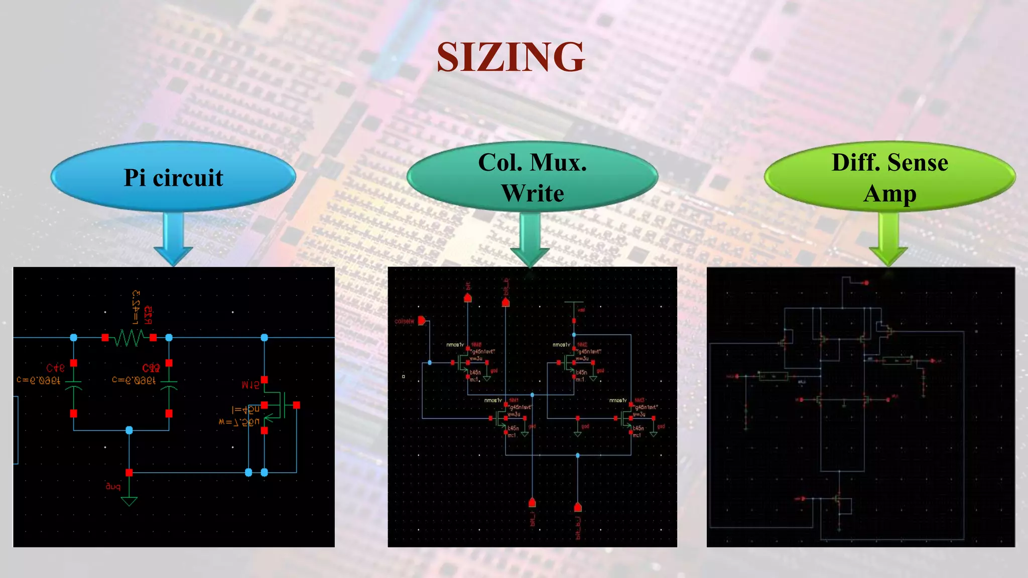
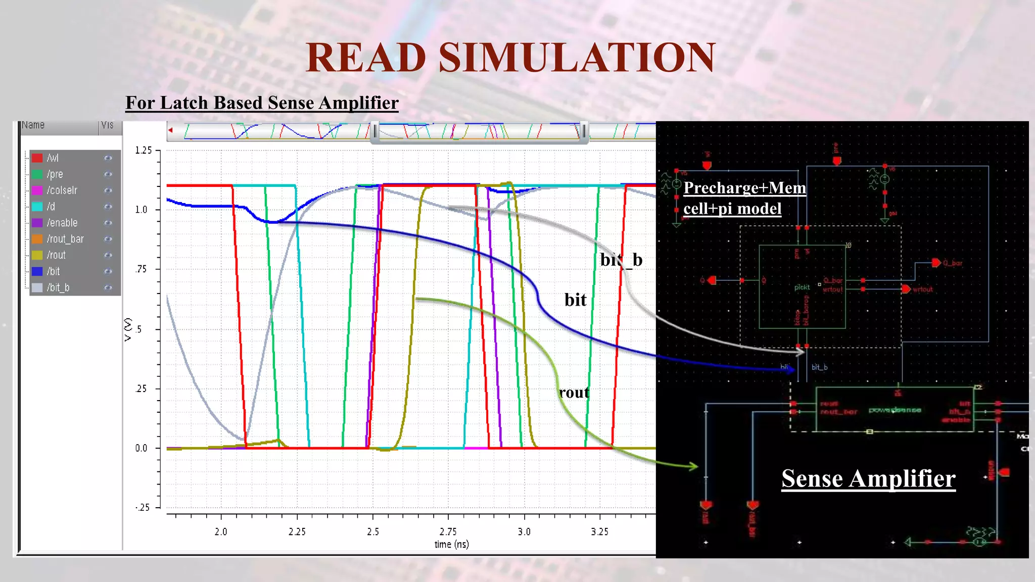
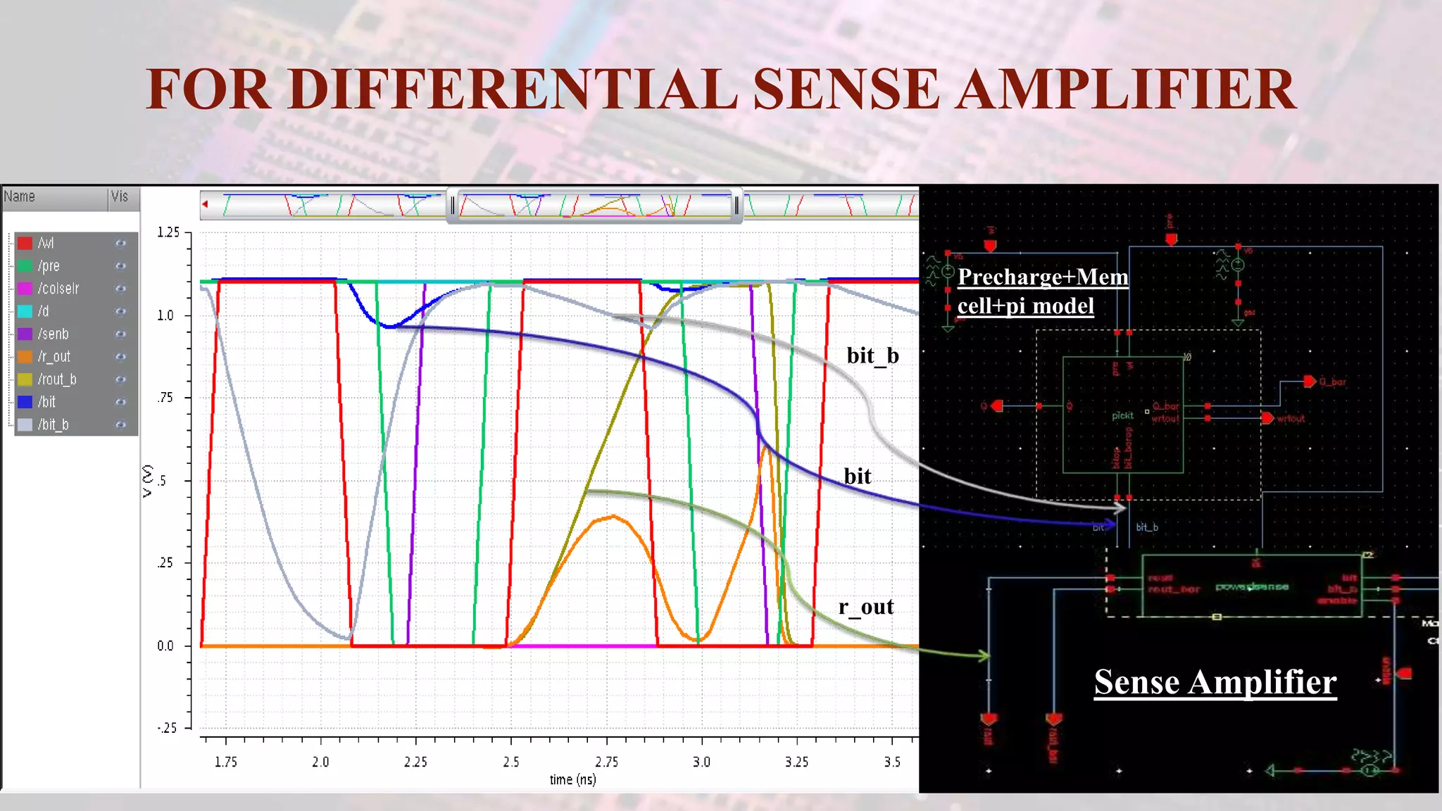
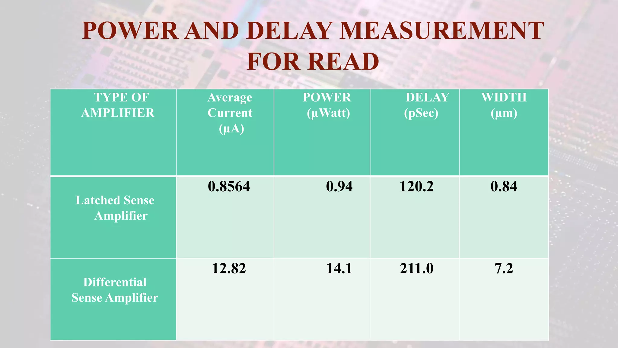
Under The Supervision of
Prof. Krishanu Datta
Department of Electronics and
Communication
Heritage Institute of Technology
VLSI SRAM READ, WRITE OPERATION
AND SENSE AMPLIFIER STUDY
•ABRARUL HAQUE (125243)
•DEBASMITA SIKDER (125222)
•JAYEESHA CHAKRABORTY (125241)
•SOUMYAJIT LANGAL (125239
Presented By:
LITERATURE SURVEY
• In the initial phase of our project we had gone through several articles from
the web resources.
• For better understanding we have gone through “CMOS VLSI Design
A Circuits and Systems Perspective” by Weste Harris Banerjee.
• And after all we are highly grateful to our mentor
Prof. Krishanu Datta for the detailed and complete understanding of our
project.
• Focus to design : 32 KB SRAM memory array
• Memory Size : 512*512 (512 rows & 512 columns)
• Tool used : Cadence Virtuoso
• Technology used : Cadence gpdk45nm
• Supply Voltage applied : 1.1V
• Comparative Study : a) Differential Sense Amplifier
VS.
b) Latch Based Sense Amplifier
• Key Parameters to analyze performance :
a) Access time
b) Speed
c) Power consumption
PROJECT OVERVIEW
6 TRANSISTOR SRAM CELL
SRAM MEMORY ARCHITECTURE
ROW DECODER AND COLUMN DECODER
CRITICAL PATH MODELLING
Schematics to be designed on the critical path :
 Precharge circuit
 RC model for bitline and bitline_bar
 Column multiplexer for write operation
 Write enable circuit
 Column multiplexer for read operation
 Sense Amplifier
For write operation
For read operation
PRECHARGE CIRCUIT
RC MODELLING OF BIT LINES
PROBLEM
How to model 512 bit line
segments on a single
column ??
OPTIMUM SOLUTION
Grouping 64 such bit line
segment to form a segment and
8 such segments
SOLUTION 2
Grouping 512 bit line segments
to an equivalent one
Equivalent bit line
represented using Pi
model and source to
drain capacitance of
NMOS
SOLUTION 1
Modeling for each of 512 bit line
segments
SPECIFICATIONS GIVEN
Parameter Value
Channel length(L) of Memory
cell MOS
45nm
Channel width(W) of Memory
cell MOS
120nm
Area Formula L=√A/12
Resistance for mid-level wire 1.01 Ω/ µm for 50nm
Capacitance for mid-level wire 0.294 fF/ µm for 50nm
CALCULATION FOR MODELING
Sl.
No.
Name of the parameter Specification
1. Cell Area (A) A=X2=144*L2 =144* 45nm2
2. Length of each side of the cell (X=√A) X=0.54 µm
3. Using 20% guard band(X´=1.2*X) X´=0.648 µm
4. Bitline length per segment (grouped by 64 cells) 64*0.648 µm = 41.472 µm
5. Resistance of Bitline per segment (grouped by 64 cells) 41.472*1.01 Ω=42.3 Ω
6. Capacitance of Bitline per segment: 41.472*0.294 fF=12.1927 fF
7. Source to drain capacitance of pass transistor w=120n*64=7.68u, l=45n
RC MODELLING
8 such
segments
COLUMN MULTIPLEXER FOR WRITE
Input/Output
Buffer
WRITE ENABLE CIRCUIT
wrt =1 to
enable AND
gate
WRITE STABILITY
For successful write operation PMOS PM5 must be weaker than the access transistor NM8.
So size of PM5 ≤ size of NM8
COLUMN MULTIPLEXER FOR READ
READ STABILITY
To read successfully from the cell the driver NM5 must be stronger than the access transistor NM7.
So size of NM4 ≥ size of NM7
SRAM without Sense
Amp
SRAM with Sense Amp
SENSE AMPLIFIER
TYPES OF SENSE AMPLIFIER
SENSE
AMPLIFIER
DIFFERENTIAL LATCHED
DIFFERENTIAL SENSE AMPLIFIER
Current source
senb
bit bit_b
rout
rout_b
LATCH BASED SENSE AMPLIFIER
CRITICAL PATH SCHEMATIC
SIMULATION & RESULTS
• The constraints are as follows
a) Timing of control signals
b) Sizing of NMOS & PMOS in critical path
• Results include 2 measurements in case of both the sense amplifiers during read operation.
a) Delay (the time lag between the wordline activation and
the Output from sense amplifier)
b)Power (during read operation the amount of power that is
consumed by the sense amplifier)
TIMING DIAGRAM
Parameter Logic State
Precharge (pre) Active Low
Wordline (wl) Active High
Multiplexer enable for
write (colselw) Active High
Write circuit enable
(wrenb) Active High
Multiplexer enable for
read (colselr) Active Low
Sense Amplifier enable
(senb) Active High
For Latched Sense Amplifier
For Differential Sense Amplifier
Write ReadInitialize
ReadWriteInitialize
SIZING
Pi circuit
Col. Mux.
Write
Diff. Sense
Amp
READ SIMULATION
For Latch Based Sense Amplifier
bit
bit_b
rout
Precharge+Mem
cell+pi model
Sense Amplifier
FOR DIFFERENTIAL SENSE AMPLIFIER
r_out
bit_b
bit
Precharge+Mem
cell+pi model
Sense Amplifier
POWER AND DELAY MEASUREMENT
FOR READ
TYPE OF
AMPLIFIER
Average
Current
(µA)
POWER
(µWatt)
DELAY
(pSec)
WIDTH
(µm)
Latched Sense
Amplifier
0.8564 0.94 120.2 0.84
Differential
Sense Amplifier
12.82 14.1 211.0 7.2
CONCLUSION
Latched base consume 14X less power.
Latched based has less READ delay.
Latched based has less size.
LATCHED DIFFERENTIALVS.
LATCHED BASE IS
THE BEST
SRAM read and write and sense amplifier

SRAM read and write and sense amplifier

  • 1.
    Under The Supervisionof Prof. Krishanu Datta Department of Electronics and Communication Heritage Institute of Technology VLSI SRAM READ, WRITE OPERATION AND SENSE AMPLIFIER STUDY
  • 2.
    •ABRARUL HAQUE (125243) •DEBASMITASIKDER (125222) •JAYEESHA CHAKRABORTY (125241) •SOUMYAJIT LANGAL (125239 Presented By:
  • 3.
    LITERATURE SURVEY • Inthe initial phase of our project we had gone through several articles from the web resources. • For better understanding we have gone through “CMOS VLSI Design A Circuits and Systems Perspective” by Weste Harris Banerjee. • And after all we are highly grateful to our mentor Prof. Krishanu Datta for the detailed and complete understanding of our project.
  • 4.
    • Focus todesign : 32 KB SRAM memory array • Memory Size : 512*512 (512 rows & 512 columns) • Tool used : Cadence Virtuoso • Technology used : Cadence gpdk45nm • Supply Voltage applied : 1.1V • Comparative Study : a) Differential Sense Amplifier VS. b) Latch Based Sense Amplifier • Key Parameters to analyze performance : a) Access time b) Speed c) Power consumption PROJECT OVERVIEW
  • 5.
  • 6.
  • 7.
    ROW DECODER ANDCOLUMN DECODER
  • 8.
    CRITICAL PATH MODELLING Schematicsto be designed on the critical path :  Precharge circuit  RC model for bitline and bitline_bar  Column multiplexer for write operation  Write enable circuit  Column multiplexer for read operation  Sense Amplifier For write operation For read operation
  • 9.
  • 10.
    RC MODELLING OFBIT LINES PROBLEM How to model 512 bit line segments on a single column ?? OPTIMUM SOLUTION Grouping 64 such bit line segment to form a segment and 8 such segments SOLUTION 2 Grouping 512 bit line segments to an equivalent one Equivalent bit line represented using Pi model and source to drain capacitance of NMOS SOLUTION 1 Modeling for each of 512 bit line segments
  • 11.
    SPECIFICATIONS GIVEN Parameter Value Channellength(L) of Memory cell MOS 45nm Channel width(W) of Memory cell MOS 120nm Area Formula L=√A/12 Resistance for mid-level wire 1.01 Ω/ µm for 50nm Capacitance for mid-level wire 0.294 fF/ µm for 50nm
  • 12.
    CALCULATION FOR MODELING Sl. No. Nameof the parameter Specification 1. Cell Area (A) A=X2=144*L2 =144* 45nm2 2. Length of each side of the cell (X=√A) X=0.54 µm 3. Using 20% guard band(X´=1.2*X) X´=0.648 µm 4. Bitline length per segment (grouped by 64 cells) 64*0.648 µm = 41.472 µm 5. Resistance of Bitline per segment (grouped by 64 cells) 41.472*1.01 Ω=42.3 Ω 6. Capacitance of Bitline per segment: 41.472*0.294 fF=12.1927 fF 7. Source to drain capacitance of pass transistor w=120n*64=7.68u, l=45n
  • 13.
  • 14.
    COLUMN MULTIPLEXER FORWRITE Input/Output Buffer
  • 15.
    WRITE ENABLE CIRCUIT wrt=1 to enable AND gate
  • 16.
    WRITE STABILITY For successfulwrite operation PMOS PM5 must be weaker than the access transistor NM8. So size of PM5 ≤ size of NM8
  • 17.
  • 18.
    READ STABILITY To readsuccessfully from the cell the driver NM5 must be stronger than the access transistor NM7. So size of NM4 ≥ size of NM7
  • 19.
    SRAM without Sense Amp SRAMwith Sense Amp SENSE AMPLIFIER
  • 20.
    TYPES OF SENSEAMPLIFIER SENSE AMPLIFIER DIFFERENTIAL LATCHED
  • 21.
    DIFFERENTIAL SENSE AMPLIFIER Currentsource senb bit bit_b rout rout_b
  • 22.
  • 23.
  • 24.
    SIMULATION & RESULTS •The constraints are as follows a) Timing of control signals b) Sizing of NMOS & PMOS in critical path • Results include 2 measurements in case of both the sense amplifiers during read operation. a) Delay (the time lag between the wordline activation and the Output from sense amplifier) b)Power (during read operation the amount of power that is consumed by the sense amplifier)
  • 25.
    TIMING DIAGRAM Parameter LogicState Precharge (pre) Active Low Wordline (wl) Active High Multiplexer enable for write (colselw) Active High Write circuit enable (wrenb) Active High Multiplexer enable for read (colselr) Active Low Sense Amplifier enable (senb) Active High For Latched Sense Amplifier For Differential Sense Amplifier Write ReadInitialize ReadWriteInitialize
  • 26.
  • 27.
    READ SIMULATION For LatchBased Sense Amplifier bit bit_b rout Precharge+Mem cell+pi model Sense Amplifier
  • 28.
    FOR DIFFERENTIAL SENSEAMPLIFIER r_out bit_b bit Precharge+Mem cell+pi model Sense Amplifier
  • 29.
    POWER AND DELAYMEASUREMENT FOR READ TYPE OF AMPLIFIER Average Current (µA) POWER (µWatt) DELAY (pSec) WIDTH (µm) Latched Sense Amplifier 0.8564 0.94 120.2 0.84 Differential Sense Amplifier 12.82 14.1 211.0 7.2
  • 30.
    CONCLUSION Latched base consume14X less power. Latched based has less READ delay. Latched based has less size. LATCHED DIFFERENTIALVS. LATCHED BASE IS THE BEST