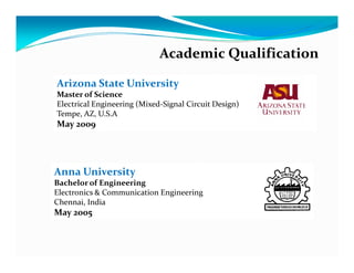
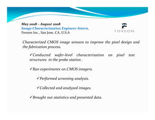
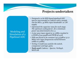
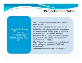
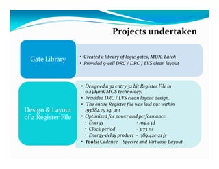
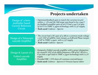
SRIRAM SUNDARRAJAH


  Professional Profile
Academic Qualification

Arizona State University
Master of Science
Electrical Engineering (Mixed-Signal Circuit Design)
Tempe, AZ, U.S.A
May 2009


Anna University
Bachelor of Engineering
Electronics & Communication Engineering
Chennai, India
May 2005
Professional Experience

May 2009 - Present
Volunteer Research Assistant for Dr. Sule Ozev,
Tempe, AZ, U.S.A


May 2008 – August 2008
Image Characterization Engineer-Intern,
San Jose, CA, U.S.A


October 2005 – July 2007
Assistant Systems Engineer,
Chennai, TN, India
May 2009 - Present
Volunteer Research Assistant for Dr. Sule Ozev,
Arizona State University, Tempe, AZ, U.S.A


Working on Defective Parts per Million (DPPM) estimation for
analog/RF circuits

         Designed an experiment (5 factors at 3 levels) using modified
      taguchi’s approach to accommodate manufacturing process
      variability of components for a LNA circuit.

         Created data and ran monte carlo (MC) simulations.

        Working on creating a database of defective parts.
May 2008 – August 2008
Image Characterization Engineer-Intern,
Foveon Inc., San Jose, CA, U.S.A

Characterized CMOS image sensors to improve the pixel design and
the fabrication process.

      Conducted wafer-level characterization       on   pixel   test
    structures in the probe station .

      Ran experiments on CMOS imagers.

          Performed screening analysis.

          Collected and analyzed images.

      Brought out statistics and presented data.
October 2005 – July 2007
Assistant Systems Engineer,
Tata Consultancy Services Ltd., Chennai, TN, India

Performed system maintenance in mainframe technology for Banking
& Financial Services client.

      Spearheaded several off-shore project deliveries with minimal
    task effort.

      Steered quarterly Releases/installations.

      Monitored smooth running of daily/weekly/monthly jobs.

      Sparked an idea to automate job flow that could save at least
    30 minutes a day for the client.
Projects undertaken

                  • Designed a 10 bit RSD-based pipelined ADC
                    spectre macromodel in Cadence with a sample
                    rate 80 MS/s, 39 MHz input bandwidth at 1.8V
                    supply.
                  • Optimized the capacitor sizes for each stage.
                    The optimum scaling factor for a minimum
                    power was determined to be 2.2.
 Modeling and
                  • A sine wave input signal at 37.71Mhz resulted in
Simulation of a     a SNDR of 59.4193dB and ENOB of 9.578
Pipelined ADC     • SNR was found to be constant (59.4233dB at 37.71
                    MHz) over input frequencies varied between
                    10Mhz to 30Mhz.
                  • Verilog A model was used for the switch,
                    comparator and logic gates.
                  • Tools used: Cadence – Spectre, VerilogA,
                    MATLAB
Projects undertaken


                    • The PFD was designed to operate at 100MHz
                      unto 250 MHz
                    • The PFD had a dead zone less than 0.16 ns
Design of a Phase   • Fully differential charge pump with minimum
                      current mismatch and variation to minimize
   Frequency          the steady state error in PLL was used.
  Detector and      • Simulated the PLL using behavioral VerilogA
charge pump for a     components. The settling time of PLL was
       PLL            determined to be 0.878 μs
                    • The PFD and the charge pump were designed
                      using 0.18 μm technology and with a 1.8 V
                      power supply.
                    • Tools used: Cadence –Spectre, VerilogA
Projects undertaken

                     • Created a library of logic gates, MUX, Latch
  Gate Library
                     • Provided 9-cell DRC / DRC / LVS clean layout


                     • Designed a 32 entry 32 bit Register File in
                       0.25dμmCMOS technology.
                     • Provided DRC / LVS clean layout design.
                     • The entire Register file was laid out within
Design & Layout        193682.79 sq. μm
of a Register File   • Optimized for power and performance.
                       • Energy                 - 104.4 pJ
                       • Clock period           - 3.73 ns
                       • Energy-delay product - 389.42e-21 Js
                     • Tools: Cadence – Spectre and Virtuoso Layout
Projects undertaken
 Design of a beta-       • Optimized feedback gain to match the currents (10 μA)
                           within +/- 5% and the Vdd range was found to be 2.399 V
  multiplier based         for feedback amplifier gain of 20V/V and 2.349 V at gain
 Current Reference         of 10V/V in TSMC 0.35μm technology, with a 2.5V supply.
      Circuit            • Tools used: Cadence – Spectre


                         • The circuit had a DC gain of 51 dB at a common mode voltage
Design of a Telescopic     1.75V, UGF of 79MHz, Gain margin 42.8 dB and Phase margin
 cascode Amplifier         of 78⁰ in TSMC 0.35μm with a 3.3V supply.
                         • Tools used: Cadence –Spectre


                         • Designed a Folded cascode amplifier with a power dissipation
Design & Layout of a       of 1.053mW, UGF of 26.2MHz frequency, PM of 63⁰, SR of 11.1
                           V/μs with a 15pF load in TSMC 0.35μm technology with a 2.7V
   Folded cascode          supply.
      Amplifier          • Provided DRC / LVS clean 2D common centroid layout.
                         • Tools used: Cadence – Spectre & Virtuoso layout editor

Professional Profile

  • 1.
    SRIRAM SUNDARRAJAH Professional Profile
  • 2.
    Academic Qualification Arizona StateUniversity Master of Science Electrical Engineering (Mixed-Signal Circuit Design) Tempe, AZ, U.S.A May 2009 Anna University Bachelor of Engineering Electronics & Communication Engineering Chennai, India May 2005
  • 3.
    Professional Experience May 2009- Present Volunteer Research Assistant for Dr. Sule Ozev, Tempe, AZ, U.S.A May 2008 – August 2008 Image Characterization Engineer-Intern, San Jose, CA, U.S.A October 2005 – July 2007 Assistant Systems Engineer, Chennai, TN, India
  • 4.
    May 2009 -Present Volunteer Research Assistant for Dr. Sule Ozev, Arizona State University, Tempe, AZ, U.S.A Working on Defective Parts per Million (DPPM) estimation for analog/RF circuits Designed an experiment (5 factors at 3 levels) using modified taguchi’s approach to accommodate manufacturing process variability of components for a LNA circuit. Created data and ran monte carlo (MC) simulations. Working on creating a database of defective parts.
  • 5.
    May 2008 –August 2008 Image Characterization Engineer-Intern, Foveon Inc., San Jose, CA, U.S.A Characterized CMOS image sensors to improve the pixel design and the fabrication process. Conducted wafer-level characterization on pixel test structures in the probe station . Ran experiments on CMOS imagers. Performed screening analysis. Collected and analyzed images. Brought out statistics and presented data.
  • 6.
    October 2005 –July 2007 Assistant Systems Engineer, Tata Consultancy Services Ltd., Chennai, TN, India Performed system maintenance in mainframe technology for Banking & Financial Services client. Spearheaded several off-shore project deliveries with minimal task effort. Steered quarterly Releases/installations. Monitored smooth running of daily/weekly/monthly jobs. Sparked an idea to automate job flow that could save at least 30 minutes a day for the client.
  • 7.
    Projects undertaken • Designed a 10 bit RSD-based pipelined ADC spectre macromodel in Cadence with a sample rate 80 MS/s, 39 MHz input bandwidth at 1.8V supply. • Optimized the capacitor sizes for each stage. The optimum scaling factor for a minimum power was determined to be 2.2. Modeling and • A sine wave input signal at 37.71Mhz resulted in Simulation of a a SNDR of 59.4193dB and ENOB of 9.578 Pipelined ADC • SNR was found to be constant (59.4233dB at 37.71 MHz) over input frequencies varied between 10Mhz to 30Mhz. • Verilog A model was used for the switch, comparator and logic gates. • Tools used: Cadence – Spectre, VerilogA, MATLAB
  • 8.
    Projects undertaken • The PFD was designed to operate at 100MHz unto 250 MHz • The PFD had a dead zone less than 0.16 ns Design of a Phase • Fully differential charge pump with minimum current mismatch and variation to minimize Frequency the steady state error in PLL was used. Detector and • Simulated the PLL using behavioral VerilogA charge pump for a components. The settling time of PLL was PLL determined to be 0.878 μs • The PFD and the charge pump were designed using 0.18 μm technology and with a 1.8 V power supply. • Tools used: Cadence –Spectre, VerilogA
  • 9.
    Projects undertaken • Created a library of logic gates, MUX, Latch Gate Library • Provided 9-cell DRC / DRC / LVS clean layout • Designed a 32 entry 32 bit Register File in 0.25dμmCMOS technology. • Provided DRC / LVS clean layout design. • The entire Register file was laid out within Design & Layout 193682.79 sq. μm of a Register File • Optimized for power and performance. • Energy - 104.4 pJ • Clock period - 3.73 ns • Energy-delay product - 389.42e-21 Js • Tools: Cadence – Spectre and Virtuoso Layout
  • 10.
    Projects undertaken Designof a beta- • Optimized feedback gain to match the currents (10 μA) within +/- 5% and the Vdd range was found to be 2.399 V multiplier based for feedback amplifier gain of 20V/V and 2.349 V at gain Current Reference of 10V/V in TSMC 0.35μm technology, with a 2.5V supply. Circuit • Tools used: Cadence – Spectre • The circuit had a DC gain of 51 dB at a common mode voltage Design of a Telescopic 1.75V, UGF of 79MHz, Gain margin 42.8 dB and Phase margin cascode Amplifier of 78⁰ in TSMC 0.35μm with a 3.3V supply. • Tools used: Cadence –Spectre • Designed a Folded cascode amplifier with a power dissipation Design & Layout of a of 1.053mW, UGF of 26.2MHz frequency, PM of 63⁰, SR of 11.1 V/μs with a 15pF load in TSMC 0.35μm technology with a 2.7V Folded cascode supply. Amplifier • Provided DRC / LVS clean 2D common centroid layout. • Tools used: Cadence – Spectre & Virtuoso layout editor