
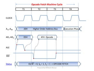
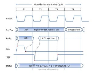
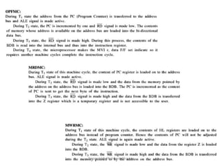
![Timing Signals For Fetching an Instruction
4F –> [MOV C, A] stored @ 2005h
T
1
T
2
T
3
T
4 Prepared By Rishikesh Bhavsar](https://image.slidesharecdn.com/chapter4-140604025400-phpapp01/85/Microprocessor-8085-Chapter-4-13-320.jpg)
![ALU
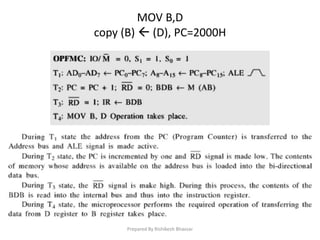
Data Flow from Memory to the MPU [4F – MOV C, A]
INSTRUCTION
DECODER
B
D E
H L
STACK
POINTER
PROGRAM
COUNTER
INTERNAL 8-BIT REGISTER
CONTROL
LOGIC
M
E
M
O
R
Y
D
E
C
O
D
E
R
4F
2000
2005
A/D BUS
2005
4F
4F
CACC External Memory
Prepared By Rishikesh Bhavsar](https://image.slidesharecdn.com/chapter4-140604025400-phpapp01/85/Microprocessor-8085-Chapter-4-15-320.jpg)
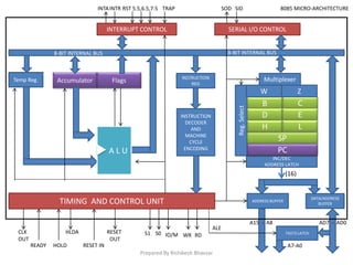
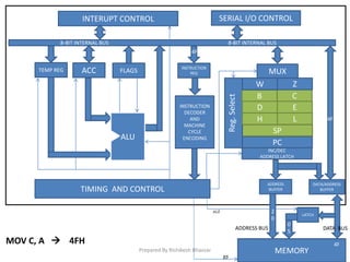
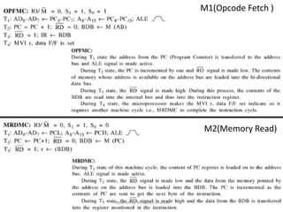


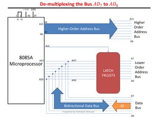
The 8085 microprocessor has 40 pins including address, data, control signals, power and clock pins. It uses multiplexed address/data bus and external latch is used to separate address and data. Memory interfacing and instruction fetch process involving program counter, memory and internal registers is explained with examples. Timing diagrams show the machine cycles and signal timings


![Interfacing technique with 8085- ADC[0808]](https://cdn.slidesharecdn.com/ss_thumbnails/adc-160307140900-thumbnail.jpg?width=640&height=640&fit=bounds)