Functional organization
•
0 likes•69 views

Functional organization of Computer Architecture

Recommended
More Related Content
What's hot
What's hot (20)
Similar to Functional organization
Similar to Functional organization (20)
More from Amit Kumar Rathi
More from Amit Kumar Rathi (20)
Recently uploaded
Recently uploaded (20)
Functional organization
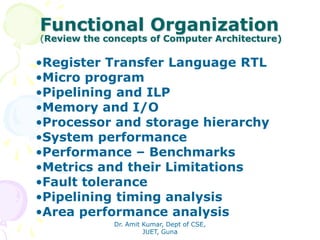
- 1. Functional Organization (Review the concepts of Computer Architecture) •Register Transfer Language RTL •Micro program •Pipelining and ILP •Memory and I/O •Processor and storage hierarchy •System performance •Performance – Benchmarks •Metrics and their Limitations •Fault tolerance •Pipelining timing analysis •Area performance analysis Dr. Amit Kumar, Dept of CSE, JUET, Guna
- 2. MICROOPERATION (2) An elementary operation performed (during one clock pulse), on the information stored in one or more registers R f(R, R) f: shift, load, clear, increment, add, subtract, complement, and, or, xor, … ALU (f) Registers (R) 1 clock cycle Register Transfer Language Dr. Amit Kumar, Dept of CSE, JUET, Guna
- 3. ORGANIZATION OF A DIGITAL SYSTEM - The Set of registers it contains and their functions -Microoperations set , the sequence of microoperation performed on binary information stored in the registers. (Set of allowable microoperations provided by the organization of the computer) -The Control signals that initiate the sequence of microoperations (to perform the functions) • Definition of the (internal) organization of a computer:- The internal hardware organization of a digital computer is best defines by specifying: Register Transfer Language Dr. Amit Kumar, Dept of CSE, JUET, Guna
- 4. REGISTER TRANSFER LEVEL Register Transfer Language • Viewing a computer, or any digital system, in this way is called the register transfer level • This is because we’re focusing on – The system’s registers – The data transformations in them, and – The data transfers between them. The term “register transfer” implies the availability of hardware logic circuits that can perform the a stated microoperation and transfer the result of the operation to the same or another register.Dr. Amit Kumar, Dept of CSE, JUET, Guna
- 5. REGISTER TRANSFER LANGUAGE (RTL) Register Transfer Language • Rather than specifying a digital system in words, a specific notation is used, register transfer language • For any function of the computer, the register transfer language can be used to describe the (sequence of) microoperations • Register transfer language – A symbolic language – A convenient tool for describing the internal organization of digital computers – Can also be used to facilitate the design process of digital systems. (The symbolic notation used to describe the microoperation transfers among registers is called a register transfer language) Dr. Amit Kumar, Dept of CSE, JUET, Guna
- 6. DESIGNATION OF REGISTERS Register Transfer Language • Registers are designated by capital letters, sometimes followed by numbers (e.g., A, R13, IR) • Often the names indicate function: – MAR - memory address register – PC - program counter – IR - instruction register • Registers and their contents can be viewed and represented in various ways – A register can be viewed as a single entity: – Registers may also be represented showing the bits of data they contain Register R MAR 1 0 1 0 0 0 1 1 Dr. Amit Kumar, Dept of CSE, JUET, Guna
- 7. DESIGNATION OF REGISTERS Register Transfer Language R1 Register Numbering of bits Showing individual bits Subfields PC(H) PC(L) 15 8 7 0 - a register - portion of a register - a bit of a register • Common ways of drawing the block diagram of a register 7 6 5 4 3 2 1 0 R2 15 0 • Designation of a register 0-7 are low byte , and 8-15 are high bit Dr. Amit Kumar, Dept of CSE, JUET, Guna
- 8. REGISTER TRANSFER Register Transfer • Information transfer (the contents) of one register to another is a register transfer. A register transfer is indicated as R2 R1 In this case the contents of register R1 are copied (loaded) into register R2. – A simultaneous transfer of all bits from the source R1 to the destination register R2, during one clock pulse. – Note that this is a non-destructive; i.e. the contents of R1 are not altered by copying (loading) them to R2 (the content of the R1 does not change after the transfer). - Known as replacement operator. Dr. Amit Kumar, Dept of CSE, JUET, Guna
- 9. REGISTER TRANSFER Register Transfer • A register transfer such as R3 R5 Implies that the digital system has – the data lines from the source register (R5) to the destination register (R3) – Parallel load capacity in the destination register R3) – Control lines to perform the action Dr. Amit Kumar, Dept of CSE, JUET, Guna
- 10. CONTROL FUNCTIONS Register Transfer • Normally, we want the transfer to occur only under a predetermined control condition. Often actions need to only occur if a certain condition is true. • This is similar to an “if” statement in a programming language. like ---- If (P= 1) then (R1 R2) • In digital systems, this is often done via a control signal, called a control function generated by control section. (P is a Boolean variable equal 0 or 1) – If the signal is 1, the action takes place • This is represented as: P: R2 R1 Which means “if P = 1, then load the contents of register R1 into register R2”, i.e., if (P = 1) then (R2 R1) Dr. Amit Kumar, Dept of CSE, JUET, Guna
- 11. HARDWARE IMPLEMENTATION OF CONTROLLED TRANSFERS Implementation of controlled transfer P: R2 R1 Block diagram Timing diagram Clock Register Transfer Transfer occurs here R2 R1 Control Circuit LoadP n Clock Load t t+1 The next positive transition of the clock at time t+1 finds the load input active and the data inputs of R2 are then loaded into the register in parallel. P may go back to 0 at time t+1, (transfer will occur with every clock pulse while P is remains active). Registers are assumed to use positive-edge-triggered flip-flops. P is activated in the control section by rising edge of a clock pulse at time t. Dr. Amit Kumar, Dept of CSE, JUET, Guna
- 12. SIMULTANEOUS OPERATIONS Register Transfer • If two or more operations are to occur simultaneously, they are separated with commas: P: R3 R5, MAR IR • Here, if the control function P = 1, load the contents of R5 into R3, and at the same time (clock), load the contents of register IR into register MAR. Dr. Amit Kumar, Dept of CSE, JUET, Guna
- 13. BASIC SYMBOLS FOR REGISTER TRANSFERS Capital letters Denotes a register MAR, R2 & numerals Parentheses () Denotes a part of a register R2(0-7), R2(L) Arrow Denotes transfer of information R2 R1 Colon : Denotes termination of control function P: Comma , Separates two micro-operations A B, R1 R2 Symbols Description Examples Register Transfer Dr. Amit Kumar, Dept of CSE, JUET, Guna
- 14. MEMORY (RAM) Bus and Memory Transfers • Memory (RAM) can be thought as a sequential circuits containing some number of registers. • These registers hold the words of memory. • Each of the r registers is indicated by an address. • These addresses range from 0 to r-1 • Each register (word) can hold n bits of data. • Assume the RAM contains r = 2k words. It needs the following – n data input lines – n data output lines – k address lines – A Read control line – A Write control line (128 x 8 RAM = 8 data input/output lines, 7 bit address lines for 128 words/registers) data input lines data output lines n n k address lines Read Write RAM unit Dr. Amit Kumar, Dept of CSE, JUET, Guna
- 15. MEMORY TRANSFER Bus and Memory Transfers • Collectively, the memory is viewed at the register level as a device, M. • Since it contains multiple locations, we must specify which address in memory we will be using. • This is done by indexing memory references. • Memory is usually accessed in computer systems by putting the desired address in a special register, the Memory Address Register (MAR, or AR). • When memory is accessed, the contents of the MAR get sent to the memory unit’s address lines AR Memory unit Read Write Data inData out M Dr. Amit Kumar, Dept of CSE, JUET, Guna
- 16. MEMORY READ Bus and Memory Transfers • To read a value from a location in memory and load it into a register, the register transfer language notation looks like this: • This causes the following to occur-- – The contents of the MAR get sent to the memory address lines. – A Read (= 1) gets sent to the memory unit. – The contents of the specified address are put on the memory’s output data lines. – These get sent over the bus to be loaded into register R1. R1 M[MAR] Dr. Amit Kumar, Dept of CSE, JUET, Guna
- 17. MEMORY WRITE Bus and Memory Transfers • To write a value from a register to a location in memory looks like this in register transfer language: • This causes the following to occur – The contents of the MAR get sent to the memory address lines. – A Write (= 1) gets sent to the memory unit. – The values in register R1 get sent over the bus to the data input lines of the memory. – The values get loaded into the specified address in the memory. M[MAR] R1 Dr. Amit Kumar, Dept of CSE, JUET, Guna
- 18. SUMMARY OF R. TRANSFER MICROOPERATIONS Bus and Memory Transfers A B Transfer content of reg. B into reg. A AR DR(AD) Transfer content of AD portion of reg. DR into reg. AR A constant Transfer a binary constant into reg. A ABUS R1, Transfer content of R1 into bus A and, at the same time, R2 ABUS transfer content of bus A into R2 AR Address register DR Data register M[R] Memory word specified by reg. R M Equivalent to M[AR] DR M Memory read operation: transfers content of memory word specified by AR into DR M DR Memory write operation: transfers content of DR into memory word specified by AR Dr. Amit Kumar, Dept of CSE, JUET, Guna
- 19. MICROOPERATIONS • Computer system microoperations are of four types: - Register transfer microoperations - Arithmetic microoperations - Logic microoperations - Shift microoperations Arithmetic Microoperations Dr. Amit Kumar, Dept of CSE, JUET, Guna
- 20. ARITHMETIC MICROOPERATIONS Summary of Typical Arithmetic Micro-Operations Arithmetic Microoperations R3 R1 + R2 Contents of R1 plus R2 transferred to R3 R3 R1 - R2 Contents of R1 minus R2 transferred to R3 R2 R2’ Complement the contents of R2 R2 R2’+ 1 2's complement the contents of R2 (negate) R3 R1 + R2’+ 1 Subtraction R1 R1 + 1 Increment R1 R1 - 1 Decrement • The basic arithmetic microoperations are – Addition – Subtraction – Increment – Decrement Dr. Amit Kumar, Dept of CSE, JUET, Guna
- 21. HALF Adder A combinational circuit that performs the arithmetic addition of two bits is called a half-adder . One that performs the addition of three bits (two significant bits and a previous carry) is called a full-adder. Two half adder are needed to implement a full adder. HALF ADDER: The input variables of a half adder are called the augend and addend bits. The output variables the sum and carry. X Y C S 0 0 0 0 0 1 0 1 1 0 0 1 1 1 1 0 The Boolean function can be obtained directly from the truth table : S = x’y + xy’ = x y C = xy Dr. Amit Kumar, Dept of CSE, JUET, Guna
- 22. FULL Adder It consists of three inputs and two outputs . Two of the inputs variables, denoted by x and y, represents the two significant bits to be added . The third input z represents the carry from the previous lower significant bit position. The two Boolean expression for the full adder : S = x y z C = xy + (x y )z x y z c s 0 0 0 0 0 0 0 1 0 1 0 1 0 0 1 0 1 1 1 0 1 0 0 0 1 1 0 1 1 0 1 1 0 1 0 1 1 1 1 1 Dr. Amit Kumar, Dept of CSE, JUET, Guna
- 23. BINARY ADDER / SUBTRACTOR / INCREMENTER FA B0 A0 S0 C0FA B1 A1 S1 C1FA B2 A2 S2 C2FA B3 A3 S3 C3 C4 Binary Adder-Subtractor FA B0 A0 S0 C0C1FA B1 A1 S1 C2FA B2 A2 S2 C3FA B3 A3 S3C4 M Binary Incrementer HA x y C S A0 1 S0 HA x y C S A1 S1 HA x y C S A2 S2 HA x y C S A3 S3C4 Binary Adder Arithmetic Microoperations (4 bit binary adder) Mode input M=0 adder M=1 subtractor When M =0 , then B 0 =B When M = 1 then we have B 1 = B’ and carry C0 = 1 Dr. Amit Kumar, Dept of CSE, JUET, Guna
- 24. ARITHMETIC CIRCUIT S1 S0 0 1 2 3 4x1 MUX X0 Y0 C0 C1 D0 FA S1 S0 0 1 2 3 4x1 MUX X1 Y1 C1 C2 D1FA S1 S0 0 1 2 3 4x1 MUX X2 Y2 C2 C3 D2FA S1 S0 0 1 2 3 4x1 MUX X3 Y3 C3 C4 D3FA Cout A0 B0 A1 B1 A2 B2 A3 B3 0 1 S0 S1 Cin S1 S0 Cin Y Output Microoperation 0 0 0 B D = A + B Add 0 0 1 B D = A + B + 1 Add with carry 0 1 0 B’ D = A + B’ Subtract with borrow 0 1 1 B’ D = A + B’+ 1 Subtract 1 0 0 0 D = A Transfer A 1 0 1 0 D = A + 1 Increment A 1 1 0 1 D = A - 1 Decrement A 1 1 1 1 D = A Transfer A Arithmetic Microoperations Output can be calculated from D = A + Y + Cin Dr. Amit Kumar, Dept of CSE, JUET, Guna
- 25. LOGIC MICROOPERATIONS Logic Microoperations • Specify binary operations on the strings of bits in registers – Logic microoperations are bit-wise operations, i.e., they work on the individual bits of data – useful for bit manipulations on binary data – useful for making logical decisions based on the bit value • There are, in principle, 16 different logic functions that can be defined over two binary input variables • However, most systems only implement four of these – AND (), OR (), XOR (), Complement/NOT • The others can be created from combination of these 0 0 0 0 0 … 1 1 1 0 1 0 0 0 … 1 1 1 1 0 0 0 1 … 0 1 1 1 1 0 1 0 … 1 0 1 A B F0 F1 F2 … F13 F14 F15 Dr. Amit Kumar, Dept of CSE, JUET, Guna
- 26. LIST OF LOGIC MICROOPERATIONS • List of Logic Microoperations - 16 different logic operations with 2 binary vars. - n binary vars → functions2 2 n • Truth tables for 16 functions of 2 variables and the corresponding 16 logic micro-operations Boolean Function Micro- Operations Name x 0 0 1 1 y 0 1 0 1 Logic Microoperations 0 0 0 0 F0 = 0 F 0 Clear 0 0 0 1 F1 = xy F A B AND 0 0 1 0 F2 = xy' F A B’ 0 0 1 1 F3 = x F A Transfer A 0 1 0 0 F4 = x'y F A’ B 0 1 0 1 F5 = y F B Transfer B 0 1 1 0 F6 = x y F A B Exclusive-OR 0 1 1 1 F7 = x + y F A B OR 1 0 0 0 F8 = (x + y)' F A B)’ NOR 1 0 0 1 F9 = (x y)' F (A B)’ Exclusive-NOR 1 0 1 0 F10 = y' F B’ Complement B 1 0 1 1 F11 = x + y' F A B 1 1 0 0 F12 = x' F A’ Complement A 1 1 0 1 F13 = x' + y F A’ B 1 1 1 0 F14 = (xy)' F (A B)’ NAND 1 1 1 1 F15 = 1 F all 1's Set to all 1's Dr. Amit Kumar, Dept of CSE, JUET, Guna
- 27. HARDWARE IMPLEMENTATION OF LOGIC MICROOPERATIONS 0 0 F = A B AND 0 1 F = AB OR 1 0 F = A B XOR 1 1 F = A’ Complement S1 S0 Output -operation Function table Logic Microoperations B A S S F 1 0 i i i 0 1 2 3 4 X 1 MUX Select There are 16 logic microoperations, most computers use only four- AND, OR, XOR, and complement. Dr. Amit Kumar, Dept of CSE, JUET, Guna
- 28. SHIFT MICROOPERATIONS Shift Microoperations • There are three types of shifts – Logical shift (left and right) – Circular shift (left and right) – Arithmetic shift (left and right) • What differentiates them is the information that goes into the serial input Serial input • A right shift operation • A left shift operation Serial input Dr. Amit Kumar, Dept of CSE, JUET, Guna
- 29. LOGICAL SHIFT Shift Microoperations • In a logical shift the serial input to the shift is a 0. • A right logical shift operation: • A left logical shift operation: • In a Register Transfer Language, the following notation is used – shl for a logical shift left – shr for a logical shift right – Examples: • R2 shr R2 (R2 = 1010) after shr = 0101 • R3 shl R3 (R3 = 0110) after shl = 1100 0 0 Dr. Amit Kumar, Dept of CSE, JUET, Guna
- 30. CIRCULAR SHIFT Shift Microoperations • In a circular shift the serial input is the bit that is shifted out of the other end of the register. • A right circular shift operation: • A left circular shift operation: • In a RTL, the following notation is used – cil for a circular shift left – cir for a circular shift right – Examples: • R2 cir R2 (R2 = 1001 after cir = 1100) • R3 cil R3 (R3 = 1011 after cil = 0111) Dr. Amit Kumar, Dept of CSE, JUET, Guna
- 31. ARITHMETIC SHIFT Shift Microoperations • An arithmetic shift is meant for signed binary numbers (integer) • An arithmetic left shift multiplies a signed number by two • An arithmetic right shift divides a signed number by two • The main distinction of an arithmetic shift is that it must keep the sign of the number the same as it performs the multiplication or division • A right arithmetic shift operation: • A left arithmetic shift operation: 0 sign bit sign bit Dr. Amit Kumar, Dept of CSE, JUET, Guna
- 32. ARITHMETIC SHIFT Shift Microoperations • An left arithmetic shift operation must be checked for the overflow 0 V Before the shift, if the leftmost two bits differ, the shift will result in an Overflow (V s the overflow flip-flop ) • In a RTL, the following notation is used – ashl for an arithmetic shift left – ashr for an arithmetic shift right – Examples: • R2 ashr R2 (R2 = 1001 after ashr = 1100) • R3 ashl R3 (R3 = 0110 after ashl = 1100) sign bit Dr. Amit Kumar, Dept of CSE, JUET, Guna
- 33. HARDWARE IMPLEMENTATION OF SHIFT MICROOPERATIONS Shift Microoperations S 0 1 H0MUX S 0 1 H1MUX S 0 1 H2MUX S 0 1 H3MUX Select 0 for shift right (down) 1 for shift left (up)Serial input (IR) A0 A1 A2 A3 Serial input (IL) Function Table Select Output S H0 H1 H2 H3 0 IR A0 A1 A2 1 A1 A2 A3 IL Dr. Amit Kumar, Dept of CSE, JUET, Guna
- 34. ARITHMETIC LOGIC SHIFT UNIT S3 S2 S1 S0 Cin Operation Function 0 0 0 0 0 F = A Transfer A 0 0 0 0 1 F = A + 1 Increment A 0 0 0 1 0 F = A + B Addition 0 0 0 1 1 F = A + B + 1 Add with carry 0 0 1 0 0 F = A + B’ Subtract with borrow 0 0 1 0 1 F = A + B’+ 1 Subtraction 0 0 1 1 0 F = A - 1 Decrement A 0 0 1 1 1 F = A TransferA 0 1 0 0 X F = A B AND 0 1 0 1 X F = A B OR 0 1 1 0 X F = A B XOR 0 1 1 1 X F = A’ Complement A 1 0 X X X F = shr A Shift right A into F 1 1 X X X F = shl A Shift left A into F Shift Microoperations Arithmetic Circuit Logic Circuit C C 4 x 1 MUX Select 0 1 2 3 F S3 S2 S1 S0 B A i A D A E shr shl i+1 i i i i+1 i-1 i i Dr. Amit Kumar, Dept of CSE, JUET, Guna