SlideShare a Scribd company logo
1 of 31
ARM
Organization and Implementation
Submitted To: Submitted By:
Dr. Nitesh Kashyap Faizan Ansari
Yash Valia
Rohit Kumar Tripathi
Shubham Singh
Ravinder Kumar
MTech VLSI Design
ARM organization
• Register file –
• 2 read ports, 1 write port +
1 read, 1 write port reserved for r15 (pc)
• Barrel shifter – shift or rotate one
operand for any number of bits
• ALU – performs the arithmetic and logic
functions required
• Memory address register + incrementer
• Memory data registers
• Instruction decoder and associated
control logic
2
multiply
data out register
instruction
decode
&
control
incrementer
register
bank
address register
barrel
shifter
A[31:0]
D[31:0]
data in register
ALU
control
P
C
PC
A
L
U
b
u
s
A
b
u
s
B
b
u
s
register
Three-stage pipeline
• Fetch
• the instruction is fetched from memory and placed in the instruction pipeline
• Decode
• the instruction is decoded and the datapath control signals prepared for the
next cycle; in this stage the instruction owns the decode logic but not the
datapath
• Execute
• the instruction owns the datapath; the register bank is read, an operand
shifted, the ALU register generated and written back into a destination
register
3
ARM single-cycle instruction pipeline
4
fetch decode execute
time
1
fetch decode execute
2
3
instruction
HAZARDS
Any conditions that causes a pipeline to
stall…
• Structural Hazard
• Data Hazard
• Control Hazard
Structural Hazard
A structural hazard occurs when two (or more) instructions
that are already in pipeline need the same resource. One
solution to such resource hazard is to increase available
resources, such as having multiple ports into main memory and
multiple (ALU) units.
Data Hazard
Data Hazard occur when instructions that exhibit
data dependency modify data in different stages
of pipeline.
ADD R1,R2 ADD R1,R2
AND R0,R1 AND R4,R3
Control Hazard
Control Hazards occur when there is a branch
instructions.
ARM Implementation
• Datapath
• RTL (Register Transfer Level)
• Control unit
• FSM (Finite State Machine)
9
2-phase non-overlapping clock scheme
• Most ARMs do not operate on edge-sensitive registers
• Instead the design is based around
2-phase non-overlapping clocks which are generated internally from
a single clock signal
• Data movement is controlled by passing the data alternatively
through latches
which are open during phase 1 or latches during phase 2
10
1 clock cycle
phase 1
phase 2
ARM datapath timing
• Register read
• Register read buses – dynamic, precharged during phase 2
• During phase 1 selected registers discharge the read buses
which become valid early in phase 1
• Shift operation
• second operand passes through barrel shifter
• ALU operation
• ALU has input latches which are open in phase 1,
allowing the operands to begin combining in ALU
as soon as they are valid, but they close at the end of phase 1
so that the phase 2 precharge does not get through to the ALU
• ALU processes the operands during the phase 2, producing the valid output
towards the end of the phase
• the result is latched in the destination register
at the end of phase 2
11
ARM datapath timing (cont’d)
12
read bus valid
shift out valid
ALU out
shift time
ALU time
register
w rite time
register
read
time
ALU operands
latched
phase1
phase2
precharge
invalidates
buses
Minimum Datapath Delay =
Register read time +
Shifter Delay + ALU Delay +
Register write set-up time + Phase 2 to phase 1 non-overlap time
The ARM6 ALU organization
• Not easy to merge the arithmetic and logic functions =>
a separate logic unit runs in parallel with the adder,
and multiplexor selects the output
13
Z
N
V
C
logic/arithmetic
C in
function
invert A invert B
result
result mux
logic functions
A operand latch B operand latch
XOR gates XOR gates
adder
zero detect
The cross-bar switch barrel shifter
• Shifter delay is critical since it contributes directly to the datapath
cycle time
• Cross-bar switch matrix (32 x 32)
• Principle for 4x4 matrix
14
in[0]
in[1]
in[2]
in[3]
out[0]
out[1]
out[2]
out[3]
no shift
right 1
right 2
right 3
left 1
left 2
left 3
The cross-bar switch barrel shifter (cont’d)
• Precharged logic is used =>
each switch is a single NMOS transistor
• Precharging sets all outputs to logic 0, so those which are not
connected to any input during switching remain at 0 giving the zero
filling required by the shift semantics
15
The cross-bar switch barrel shifter (cont’d)
16
• For rotate right, the right shift diagonal is enabled +
complementary shift left diagonal (e. g., ‘right 1’ + ‘left 3’)
• Arithmetic shift right:
use sign-extension => separate logic is used to decode the shift amount and
discharge those outputs appropriately
ARM register bank
17
• ARM has 31 general Purpose Registers containing 1KB of data (32 bits).
ARM2 register cell circuit
18
A bus
B bus
ALUbus
write
read
B
read
A
• Transistor circuit of register cell used in ARM cores upto ARM6 is based on
Asymmetric Cross Coupled Paires of CMOS inverters.
• This cross coupled CMOS is overdriven by strong signal from ALU bus when
register contents are charged.
ARM2 register cell circuit
• The Feedback inverter is made weak in order to minimize the cells
Resistance to a new value.
• A and B buses are pre-charged to Vdd during phase-2 of clock cycle
so that register cells needs only discharge the read bused , which it
does through the n-type pass transistor when read lines are enabled
19
A bus
B bus
ALUbus
write
read
B
read
A
ARM register bank floor plan
20
A bus read decoders
B bus read decoders
w rite decoders
register cells
PC
Vdd
Vss
ALU
bus
PC
bus
INC
bus
ALU
bus
A bus
B bus
• Register Cells are arranged in columns to for a 32-bit register and columns are
packed together to form complete register bank.
ARM register bank floor plan
• Decoder for read and write enable lines are packed above the
columns.
• Enable line runs vertically whereas databus horizontally across the
array of register cell.
21
A bus read decoders
B bus read decoders
w rite decoders
register cells
PC
Vdd
Vss
ALU
bus
PC
bus
INC
bus
ALU
bus
A bus
B bus
ARM core datapath buses
22
address register
incrementer
register bank
multiplier
ALU
shifter
data in
instruction pipe
data out
A B
W
instruction
Din
shift out
PC
Ad
inc
• The order of datapath buses is chosen to minimize the number of additional
busses passing over more complex functions.
Buses:
1. Register bank output buses(A,B)
2. Data/Inst. Input buses(Din)
3. Data write bus(W)
4. Address incrementation bus(Ad)
5. Data/Addr incremetation
bus(Inc)
6. PC load (PC)
7. Shift out
ARM control logic structure
23
decode
PLA
cycle
count
multiply
control
load/store
multiple
address
control
register
control
ALU
control
shifter
control
instruction
coprocessor
The Control Path in simpler
ARM cores has 3 structural
components :-
1. An instruction Decoder
PLA
2. Distributed secondary
control associated with
main functional units.
3. Decentralized control
units for specific
instruction
ARM Instruction Execution
DATA PROCESSING INSTRUCTIONS
• A data processing instruction requires two operands, one of which is
always a register and the other is either a second register or an
immediate value.
• The second operand is passed through the barrel shifter where it is
subject to a general shift operation, then it is combined with the first
operand in the ALU using a general ALU operation. Finally, the result
from the ALU is written back into the destination register.
• The PC value in the address register is incremented and copied back
into both the address register and r15 in the register bank.
DATAPATH ACTIVITY
Reg-Reg
Rd = Rn op Rm
r15 = AR + 4
AR = AR + 4
Reg-Imm
Rd = Rn op Imm
r15 = AR + 4
AR = AR + 4
DATA TRANSFER INSTRUCTIONS
• A data transfer (load or store) instruction computes a memory
address in which register is used as the base address, to which is
added (or from which is subtracted) an offset which again may be
another register or an immediate value.
• The address is sent to the address register, and in a second cycle the
data transfer takes place.
• The incremented PC value is stored in the register bank at the end of
the first cycle so that the address register is free to accept the data
transfer address for the second cycle.
• The value sent to the address register in a cycle is the value used for
the memory access in the following cycle.
• The address register is, in effect, a pipeline register between the
processor datapath and the external memory.
STORE INSTRUCTION DATAPATH ACTIVITY
Compute
address
AR = Rn op
Disp
r15 = AR + 4
Store data
AR = PC
mem[AR] =
Rd<x:y>
BRANCHING INSTRUCTIONS
• Branch instructions compute the target address in the first cycle.
• A 24-bit immediate field is extracted from the instruction and then
shifted left two bit positions to give a word-aligned offset which is
added to the PC. The result is issued as an instruction fetch address,
and while the instruction pipeline refills the return address is copied
into the link register (r14).
• The third cycle, which is required to complete the pipeline refilling, is
also used to make a small correction to the value stored in the link
register in order that it points directly at the instruction which follows
the branch.
TWO CYCLE OF BRANCH INSTRUCTION
Compute target
address
AR = PC + Disp,lsl
#2
Save return address
(if required)
r14 = PC
AR = AR + 4
31
Thank You

More Related Content

What's hot

Introduction to Digital Signal processors
Introduction to Digital Signal processorsIntroduction to Digital Signal processors
Introduction to Digital Signal processorsPeriyanayagiS
 
Embedded system in Smart Cards
Embedded system in Smart CardsEmbedded system in Smart Cards
Embedded system in Smart CardsRebecca D'souza
 
Arm programmer's model
Arm programmer's modelArm programmer's model
Arm programmer's modelv Kalairajan
 
Architectural support for High Level Language
Architectural support for High Level LanguageArchitectural support for High Level Language
Architectural support for High Level LanguageSudhanshu Janwadkar
 
8259 Programmable Interrupt Controller
8259 Programmable Interrupt Controller8259 Programmable Interrupt Controller
8259 Programmable Interrupt Controllerabhikalmegh
 
Instruction cycle with interrupts
Instruction cycle with interruptsInstruction cycle with interrupts
Instruction cycle with interruptsShubham Jain
 
8237 dma controller
8237 dma controller8237 dma controller
8237 dma controllerTech_MX
 
System On Chip
System On ChipSystem On Chip
System On ChipA B Shinde
 
Arm architecture chapter2_steve_furber
Arm architecture chapter2_steve_furberArm architecture chapter2_steve_furber
Arm architecture chapter2_steve_furberasodariyabhavesh
 
Unit II arm 7 Instruction Set
Unit II arm 7 Instruction SetUnit II arm 7 Instruction Set
Unit II arm 7 Instruction SetDr. Pankaj Zope
 
Architecture of 8086 Microprocessor
Architecture of 8086 Microprocessor  Architecture of 8086 Microprocessor
Architecture of 8086 Microprocessor Mustapha Fatty
 

What's hot (20)

Introduction to Digital Signal processors
Introduction to Digital Signal processorsIntroduction to Digital Signal processors
Introduction to Digital Signal processors
 
ARM Processors
ARM ProcessorsARM Processors
ARM Processors
 
Embedded system in Smart Cards
Embedded system in Smart CardsEmbedded system in Smart Cards
Embedded system in Smart Cards
 
Multipliers in VLSI
Multipliers in VLSIMultipliers in VLSI
Multipliers in VLSI
 
Arm programmer's model
Arm programmer's modelArm programmer's model
Arm programmer's model
 
Architectural support for High Level Language
Architectural support for High Level LanguageArchitectural support for High Level Language
Architectural support for High Level Language
 
8259 Programmable Interrupt Controller
8259 Programmable Interrupt Controller8259 Programmable Interrupt Controller
8259 Programmable Interrupt Controller
 
Arm instruction set
Arm instruction setArm instruction set
Arm instruction set
 
Instruction cycle with interrupts
Instruction cycle with interruptsInstruction cycle with interrupts
Instruction cycle with interrupts
 
8237 dma controller
8237 dma controller8237 dma controller
8237 dma controller
 
ARM Architecture
ARM ArchitectureARM Architecture
ARM Architecture
 
UART
UARTUART
UART
 
System On Chip
System On ChipSystem On Chip
System On Chip
 
Arm architecture chapter2_steve_furber
Arm architecture chapter2_steve_furberArm architecture chapter2_steve_furber
Arm architecture chapter2_steve_furber
 
dual-port RAM (DPRAM)
dual-port RAM (DPRAM)dual-port RAM (DPRAM)
dual-port RAM (DPRAM)
 
Unit II arm 7 Instruction Set
Unit II arm 7 Instruction SetUnit II arm 7 Instruction Set
Unit II arm 7 Instruction Set
 
ARM CORTEX M3 PPT
ARM CORTEX M3 PPTARM CORTEX M3 PPT
ARM CORTEX M3 PPT
 
Ec8791 arm 9 processor
Ec8791 arm 9 processorEc8791 arm 9 processor
Ec8791 arm 9 processor
 
Architecture of 8086 Microprocessor
Architecture of 8086 Microprocessor  Architecture of 8086 Microprocessor
Architecture of 8086 Microprocessor
 
DMA operation
DMA operationDMA operation
DMA operation
 

Similar to Arm organization and implementation

310471266 chapter-7-notes-computer-organization
310471266 chapter-7-notes-computer-organization310471266 chapter-7-notes-computer-organization
310471266 chapter-7-notes-computer-organizationsrinoni
 
COMPUTER ORGANIZATION NOTES Unit 7
COMPUTER ORGANIZATION NOTES Unit 7COMPUTER ORGANIZATION NOTES Unit 7
COMPUTER ORGANIZATION NOTES Unit 7Dr.MAYA NAYAK
 
Computer organization prashant odhavani- 160920107003
Computer organization   prashant odhavani- 160920107003Computer organization   prashant odhavani- 160920107003
Computer organization prashant odhavani- 160920107003Prashant odhavani
 
PPT in register and micro operations in electronic
PPT in register and micro operations in electronicPPT in register and micro operations in electronic
PPT in register and micro operations in electronicaaravjamela
 
MCA-I-COA- overview of register transfer, micro operations and basic computer...
MCA-I-COA- overview of register transfer, micro operations and basic computer...MCA-I-COA- overview of register transfer, micro operations and basic computer...
MCA-I-COA- overview of register transfer, micro operations and basic computer...Rai University
 
Bca 2nd sem-u-2.2-overview of register transfer, micro operations and basic c...
Bca 2nd sem-u-2.2-overview of register transfer, micro operations and basic c...Bca 2nd sem-u-2.2-overview of register transfer, micro operations and basic c...
Bca 2nd sem-u-2.2-overview of register transfer, micro operations and basic c...Rai University
 
B.sc cs-ii-u-2.2-overview of register transfer, micro operations and basic co...
B.sc cs-ii-u-2.2-overview of register transfer, micro operations and basic co...B.sc cs-ii-u-2.2-overview of register transfer, micro operations and basic co...
B.sc cs-ii-u-2.2-overview of register transfer, micro operations and basic co...Rai University
 

Similar to Arm organization and implementation (20)

mod 3-1.pptx
mod 3-1.pptxmod 3-1.pptx
mod 3-1.pptx
 
coa
coacoa
coa
 
310471266 chapter-7-notes-computer-organization
310471266 chapter-7-notes-computer-organization310471266 chapter-7-notes-computer-organization
310471266 chapter-7-notes-computer-organization
 
COMPUTER ORGANIZATION NOTES Unit 7
COMPUTER ORGANIZATION NOTES Unit 7COMPUTER ORGANIZATION NOTES Unit 7
COMPUTER ORGANIZATION NOTES Unit 7
 
THE PROCESSOR
THE PROCESSORTHE PROCESSOR
THE PROCESSOR
 
Digital-Unit-III.ppt
Digital-Unit-III.pptDigital-Unit-III.ppt
Digital-Unit-III.ppt
 
Unit 3 The processor
Unit 3 The processorUnit 3 The processor
Unit 3 The processor
 
8051d
8051d8051d
8051d
 
Computer Organization
Computer OrganizationComputer Organization
Computer Organization
 
Basic non pipelined cpu architecture
Basic non pipelined cpu architectureBasic non pipelined cpu architecture
Basic non pipelined cpu architecture
 
Computer organization prashant odhavani- 160920107003
Computer organization   prashant odhavani- 160920107003Computer organization   prashant odhavani- 160920107003
Computer organization prashant odhavani- 160920107003
 
COA (Unit_1.pptx)
COA (Unit_1.pptx)COA (Unit_1.pptx)
COA (Unit_1.pptx)
 
PPT in register and micro operations in electronic
PPT in register and micro operations in electronicPPT in register and micro operations in electronic
PPT in register and micro operations in electronic
 
MPMC
MPMC MPMC
MPMC
 
SUDHARSAN.V.pptx
SUDHARSAN.V.pptxSUDHARSAN.V.pptx
SUDHARSAN.V.pptx
 
MCA-I-COA- overview of register transfer, micro operations and basic computer...
MCA-I-COA- overview of register transfer, micro operations and basic computer...MCA-I-COA- overview of register transfer, micro operations and basic computer...
MCA-I-COA- overview of register transfer, micro operations and basic computer...
 
Bca 2nd sem-u-2.2-overview of register transfer, micro operations and basic c...
Bca 2nd sem-u-2.2-overview of register transfer, micro operations and basic c...Bca 2nd sem-u-2.2-overview of register transfer, micro operations and basic c...
Bca 2nd sem-u-2.2-overview of register transfer, micro operations and basic c...
 
Pentium processor
Pentium processorPentium processor
Pentium processor
 
B.sc cs-ii-u-2.2-overview of register transfer, micro operations and basic co...
B.sc cs-ii-u-2.2-overview of register transfer, micro operations and basic co...B.sc cs-ii-u-2.2-overview of register transfer, micro operations and basic co...
B.sc cs-ii-u-2.2-overview of register transfer, micro operations and basic co...
 
Unit - 5 Pipelining.pptx
Unit - 5 Pipelining.pptxUnit - 5 Pipelining.pptx
Unit - 5 Pipelining.pptx
 

Recently uploaded

Gurgaon ✡️9711147426✨Call In girls Gurgaon Sector 51 escort service
Gurgaon ✡️9711147426✨Call In girls Gurgaon Sector 51 escort serviceGurgaon ✡️9711147426✨Call In girls Gurgaon Sector 51 escort service
Gurgaon ✡️9711147426✨Call In girls Gurgaon Sector 51 escort servicejennyeacort
 
Work Experience-Dalton Park.pptxfvvvvvvv
Work Experience-Dalton Park.pptxfvvvvvvvWork Experience-Dalton Park.pptxfvvvvvvv
Work Experience-Dalton Park.pptxfvvvvvvvLewisJB
 
Past, Present and Future of Generative AI
Past, Present and Future of Generative AIPast, Present and Future of Generative AI
Past, Present and Future of Generative AIabhishek36461
 
Electronically Controlled suspensions system .pdf
Electronically Controlled suspensions system .pdfElectronically Controlled suspensions system .pdf
Electronically Controlled suspensions system .pdfme23b1001
 
Software and Systems Engineering Standards: Verification and Validation of Sy...
Software and Systems Engineering Standards: Verification and Validation of Sy...Software and Systems Engineering Standards: Verification and Validation of Sy...
Software and Systems Engineering Standards: Verification and Validation of Sy...VICTOR MAESTRE RAMIREZ
 
CCS355 Neural Networks & Deep Learning Unit 1 PDF notes with Question bank .pdf
CCS355 Neural Networks & Deep Learning Unit 1 PDF notes with Question bank .pdfCCS355 Neural Networks & Deep Learning Unit 1 PDF notes with Question bank .pdf
CCS355 Neural Networks & Deep Learning Unit 1 PDF notes with Question bank .pdfAsst.prof M.Gokilavani
 
pipeline in computer architecture design
pipeline in computer architecture  designpipeline in computer architecture  design
pipeline in computer architecture designssuser87fa0c1
 
Study on Air-Water & Water-Water Heat Exchange in a Finned Tube Exchanger
Study on Air-Water & Water-Water Heat Exchange in a Finned Tube ExchangerStudy on Air-Water & Water-Water Heat Exchange in a Finned Tube Exchanger
Study on Air-Water & Water-Water Heat Exchange in a Finned Tube ExchangerAnamika Sarkar
 
EduAI - E learning Platform integrated with AI
EduAI - E learning Platform integrated with AIEduAI - E learning Platform integrated with AI
EduAI - E learning Platform integrated with AIkoyaldeepu123
 
CCS355 Neural Network & Deep Learning UNIT III notes and Question bank .pdf
CCS355 Neural Network & Deep Learning UNIT III notes and Question bank .pdfCCS355 Neural Network & Deep Learning UNIT III notes and Question bank .pdf
CCS355 Neural Network & Deep Learning UNIT III notes and Question bank .pdfAsst.prof M.Gokilavani
 
Churning of Butter, Factors affecting .
Churning of Butter, Factors affecting  .Churning of Butter, Factors affecting  .
Churning of Butter, Factors affecting .Satyam Kumar
 
Risk Assessment For Installation of Drainage Pipes.pdf
Risk Assessment For Installation of Drainage Pipes.pdfRisk Assessment For Installation of Drainage Pipes.pdf
Risk Assessment For Installation of Drainage Pipes.pdfROCENODodongVILLACER
 
Decoding Kotlin - Your guide to solving the mysterious in Kotlin.pptx
Decoding Kotlin - Your guide to solving the mysterious in Kotlin.pptxDecoding Kotlin - Your guide to solving the mysterious in Kotlin.pptx
Decoding Kotlin - Your guide to solving the mysterious in Kotlin.pptxJoão Esperancinha
 
Introduction-To-Agricultural-Surveillance-Rover.pptx
Introduction-To-Agricultural-Surveillance-Rover.pptxIntroduction-To-Agricultural-Surveillance-Rover.pptx
Introduction-To-Agricultural-Surveillance-Rover.pptxk795866
 
GDSC ASEB Gen AI study jams presentation
GDSC ASEB Gen AI study jams presentationGDSC ASEB Gen AI study jams presentation
GDSC ASEB Gen AI study jams presentationGDSCAESB
 
Gfe Mayur Vihar Call Girls Service WhatsApp -> 9999965857 Available 24x7 ^ De...
Gfe Mayur Vihar Call Girls Service WhatsApp -> 9999965857 Available 24x7 ^ De...Gfe Mayur Vihar Call Girls Service WhatsApp -> 9999965857 Available 24x7 ^ De...
Gfe Mayur Vihar Call Girls Service WhatsApp -> 9999965857 Available 24x7 ^ De...srsj9000
 
Call Us ≽ 8377877756 ≼ Call Girls In Shastri Nagar (Delhi)
Call Us ≽ 8377877756 ≼ Call Girls In Shastri Nagar (Delhi)Call Us ≽ 8377877756 ≼ Call Girls In Shastri Nagar (Delhi)
Call Us ≽ 8377877756 ≼ Call Girls In Shastri Nagar (Delhi)dollysharma2066
 

Recently uploaded (20)

Gurgaon ✡️9711147426✨Call In girls Gurgaon Sector 51 escort service
Gurgaon ✡️9711147426✨Call In girls Gurgaon Sector 51 escort serviceGurgaon ✡️9711147426✨Call In girls Gurgaon Sector 51 escort service
Gurgaon ✡️9711147426✨Call In girls Gurgaon Sector 51 escort service
 
Work Experience-Dalton Park.pptxfvvvvvvv
Work Experience-Dalton Park.pptxfvvvvvvvWork Experience-Dalton Park.pptxfvvvvvvv
Work Experience-Dalton Park.pptxfvvvvvvv
 
Past, Present and Future of Generative AI
Past, Present and Future of Generative AIPast, Present and Future of Generative AI
Past, Present and Future of Generative AI
 
9953056974 Call Girls In South Ex, Escorts (Delhi) NCR.pdf
9953056974 Call Girls In South Ex, Escorts (Delhi) NCR.pdf9953056974 Call Girls In South Ex, Escorts (Delhi) NCR.pdf
9953056974 Call Girls In South Ex, Escorts (Delhi) NCR.pdf
 
Electronically Controlled suspensions system .pdf
Electronically Controlled suspensions system .pdfElectronically Controlled suspensions system .pdf
Electronically Controlled suspensions system .pdf
 
Software and Systems Engineering Standards: Verification and Validation of Sy...
Software and Systems Engineering Standards: Verification and Validation of Sy...Software and Systems Engineering Standards: Verification and Validation of Sy...
Software and Systems Engineering Standards: Verification and Validation of Sy...
 
CCS355 Neural Networks & Deep Learning Unit 1 PDF notes with Question bank .pdf
CCS355 Neural Networks & Deep Learning Unit 1 PDF notes with Question bank .pdfCCS355 Neural Networks & Deep Learning Unit 1 PDF notes with Question bank .pdf
CCS355 Neural Networks & Deep Learning Unit 1 PDF notes with Question bank .pdf
 
pipeline in computer architecture design
pipeline in computer architecture  designpipeline in computer architecture  design
pipeline in computer architecture design
 
Study on Air-Water & Water-Water Heat Exchange in a Finned Tube Exchanger
Study on Air-Water & Water-Water Heat Exchange in a Finned Tube ExchangerStudy on Air-Water & Water-Water Heat Exchange in a Finned Tube Exchanger
Study on Air-Water & Water-Water Heat Exchange in a Finned Tube Exchanger
 
EduAI - E learning Platform integrated with AI
EduAI - E learning Platform integrated with AIEduAI - E learning Platform integrated with AI
EduAI - E learning Platform integrated with AI
 
🔝9953056974🔝!!-YOUNG call girls in Rajendra Nagar Escort rvice Shot 2000 nigh...
🔝9953056974🔝!!-YOUNG call girls in Rajendra Nagar Escort rvice Shot 2000 nigh...🔝9953056974🔝!!-YOUNG call girls in Rajendra Nagar Escort rvice Shot 2000 nigh...
🔝9953056974🔝!!-YOUNG call girls in Rajendra Nagar Escort rvice Shot 2000 nigh...
 
POWER SYSTEMS-1 Complete notes examples
POWER SYSTEMS-1 Complete notes  examplesPOWER SYSTEMS-1 Complete notes  examples
POWER SYSTEMS-1 Complete notes examples
 
CCS355 Neural Network & Deep Learning UNIT III notes and Question bank .pdf
CCS355 Neural Network & Deep Learning UNIT III notes and Question bank .pdfCCS355 Neural Network & Deep Learning UNIT III notes and Question bank .pdf
CCS355 Neural Network & Deep Learning UNIT III notes and Question bank .pdf
 
Churning of Butter, Factors affecting .
Churning of Butter, Factors affecting  .Churning of Butter, Factors affecting  .
Churning of Butter, Factors affecting .
 
Risk Assessment For Installation of Drainage Pipes.pdf
Risk Assessment For Installation of Drainage Pipes.pdfRisk Assessment For Installation of Drainage Pipes.pdf
Risk Assessment For Installation of Drainage Pipes.pdf
 
Decoding Kotlin - Your guide to solving the mysterious in Kotlin.pptx
Decoding Kotlin - Your guide to solving the mysterious in Kotlin.pptxDecoding Kotlin - Your guide to solving the mysterious in Kotlin.pptx
Decoding Kotlin - Your guide to solving the mysterious in Kotlin.pptx
 
Introduction-To-Agricultural-Surveillance-Rover.pptx
Introduction-To-Agricultural-Surveillance-Rover.pptxIntroduction-To-Agricultural-Surveillance-Rover.pptx
Introduction-To-Agricultural-Surveillance-Rover.pptx
 
GDSC ASEB Gen AI study jams presentation
GDSC ASEB Gen AI study jams presentationGDSC ASEB Gen AI study jams presentation
GDSC ASEB Gen AI study jams presentation
 
Gfe Mayur Vihar Call Girls Service WhatsApp -> 9999965857 Available 24x7 ^ De...
Gfe Mayur Vihar Call Girls Service WhatsApp -> 9999965857 Available 24x7 ^ De...Gfe Mayur Vihar Call Girls Service WhatsApp -> 9999965857 Available 24x7 ^ De...
Gfe Mayur Vihar Call Girls Service WhatsApp -> 9999965857 Available 24x7 ^ De...
 
Call Us ≽ 8377877756 ≼ Call Girls In Shastri Nagar (Delhi)
Call Us ≽ 8377877756 ≼ Call Girls In Shastri Nagar (Delhi)Call Us ≽ 8377877756 ≼ Call Girls In Shastri Nagar (Delhi)
Call Us ≽ 8377877756 ≼ Call Girls In Shastri Nagar (Delhi)
 

Arm organization and implementation

  • 1. ARM Organization and Implementation Submitted To: Submitted By: Dr. Nitesh Kashyap Faizan Ansari Yash Valia Rohit Kumar Tripathi Shubham Singh Ravinder Kumar MTech VLSI Design
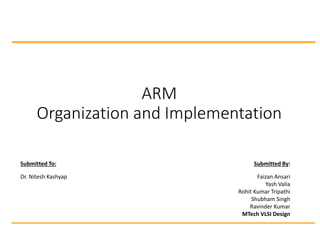
  • 2. ARM organization • Register file – • 2 read ports, 1 write port + 1 read, 1 write port reserved for r15 (pc) • Barrel shifter – shift or rotate one operand for any number of bits • ALU – performs the arithmetic and logic functions required • Memory address register + incrementer • Memory data registers • Instruction decoder and associated control logic 2 multiply data out register instruction decode & control incrementer register bank address register barrel shifter A[31:0] D[31:0] data in register ALU control P C PC A L U b u s A b u s B b u s register
  • 3. Three-stage pipeline • Fetch • the instruction is fetched from memory and placed in the instruction pipeline • Decode • the instruction is decoded and the datapath control signals prepared for the next cycle; in this stage the instruction owns the decode logic but not the datapath • Execute • the instruction owns the datapath; the register bank is read, an operand shifted, the ALU register generated and written back into a destination register 3
  • 4. ARM single-cycle instruction pipeline 4 fetch decode execute time 1 fetch decode execute fetch decode execute 2 3 instruction
  • 5. HAZARDS Any conditions that causes a pipeline to stall… • Structural Hazard • Data Hazard • Control Hazard
  • 6. Structural Hazard A structural hazard occurs when two (or more) instructions that are already in pipeline need the same resource. One solution to such resource hazard is to increase available resources, such as having multiple ports into main memory and multiple (ALU) units.
  • 7. Data Hazard Data Hazard occur when instructions that exhibit data dependency modify data in different stages of pipeline. ADD R1,R2 ADD R1,R2 AND R0,R1 AND R4,R3
  • 8. Control Hazard Control Hazards occur when there is a branch instructions.
  • 9. ARM Implementation • Datapath • RTL (Register Transfer Level) • Control unit • FSM (Finite State Machine) 9
  • 10. 2-phase non-overlapping clock scheme • Most ARMs do not operate on edge-sensitive registers • Instead the design is based around 2-phase non-overlapping clocks which are generated internally from a single clock signal • Data movement is controlled by passing the data alternatively through latches which are open during phase 1 or latches during phase 2 10 1 clock cycle phase 1 phase 2
  • 11. ARM datapath timing • Register read • Register read buses – dynamic, precharged during phase 2 • During phase 1 selected registers discharge the read buses which become valid early in phase 1 • Shift operation • second operand passes through barrel shifter • ALU operation • ALU has input latches which are open in phase 1, allowing the operands to begin combining in ALU as soon as they are valid, but they close at the end of phase 1 so that the phase 2 precharge does not get through to the ALU • ALU processes the operands during the phase 2, producing the valid output towards the end of the phase • the result is latched in the destination register at the end of phase 2 11
  • 12. ARM datapath timing (cont’d) 12 read bus valid shift out valid ALU out shift time ALU time register w rite time register read time ALU operands latched phase1 phase2 precharge invalidates buses Minimum Datapath Delay = Register read time + Shifter Delay + ALU Delay + Register write set-up time + Phase 2 to phase 1 non-overlap time
  • 13. The ARM6 ALU organization • Not easy to merge the arithmetic and logic functions => a separate logic unit runs in parallel with the adder, and multiplexor selects the output 13 Z N V C logic/arithmetic C in function invert A invert B result result mux logic functions A operand latch B operand latch XOR gates XOR gates adder zero detect
  • 14. The cross-bar switch barrel shifter • Shifter delay is critical since it contributes directly to the datapath cycle time • Cross-bar switch matrix (32 x 32) • Principle for 4x4 matrix 14 in[0] in[1] in[2] in[3] out[0] out[1] out[2] out[3] no shift right 1 right 2 right 3 left 1 left 2 left 3
  • 15. The cross-bar switch barrel shifter (cont’d) • Precharged logic is used => each switch is a single NMOS transistor • Precharging sets all outputs to logic 0, so those which are not connected to any input during switching remain at 0 giving the zero filling required by the shift semantics 15
  • 16. The cross-bar switch barrel shifter (cont’d) 16 • For rotate right, the right shift diagonal is enabled + complementary shift left diagonal (e. g., ‘right 1’ + ‘left 3’) • Arithmetic shift right: use sign-extension => separate logic is used to decode the shift amount and discharge those outputs appropriately
  • 17. ARM register bank 17 • ARM has 31 general Purpose Registers containing 1KB of data (32 bits).
  • 18. ARM2 register cell circuit 18 A bus B bus ALUbus write read B read A • Transistor circuit of register cell used in ARM cores upto ARM6 is based on Asymmetric Cross Coupled Paires of CMOS inverters. • This cross coupled CMOS is overdriven by strong signal from ALU bus when register contents are charged.
  • 19. ARM2 register cell circuit • The Feedback inverter is made weak in order to minimize the cells Resistance to a new value. • A and B buses are pre-charged to Vdd during phase-2 of clock cycle so that register cells needs only discharge the read bused , which it does through the n-type pass transistor when read lines are enabled 19 A bus B bus ALUbus write read B read A
  • 20. ARM register bank floor plan 20 A bus read decoders B bus read decoders w rite decoders register cells PC Vdd Vss ALU bus PC bus INC bus ALU bus A bus B bus • Register Cells are arranged in columns to for a 32-bit register and columns are packed together to form complete register bank.
  • 21. ARM register bank floor plan • Decoder for read and write enable lines are packed above the columns. • Enable line runs vertically whereas databus horizontally across the array of register cell. 21 A bus read decoders B bus read decoders w rite decoders register cells PC Vdd Vss ALU bus PC bus INC bus ALU bus A bus B bus
  • 22. ARM core datapath buses 22 address register incrementer register bank multiplier ALU shifter data in instruction pipe data out A B W instruction Din shift out PC Ad inc • The order of datapath buses is chosen to minimize the number of additional busses passing over more complex functions. Buses: 1. Register bank output buses(A,B) 2. Data/Inst. Input buses(Din) 3. Data write bus(W) 4. Address incrementation bus(Ad) 5. Data/Addr incremetation bus(Inc) 6. PC load (PC) 7. Shift out
  • 23. ARM control logic structure 23 decode PLA cycle count multiply control load/store multiple address control register control ALU control shifter control instruction coprocessor The Control Path in simpler ARM cores has 3 structural components :- 1. An instruction Decoder PLA 2. Distributed secondary control associated with main functional units. 3. Decentralized control units for specific instruction
  • 25. DATA PROCESSING INSTRUCTIONS • A data processing instruction requires two operands, one of which is always a register and the other is either a second register or an immediate value. • The second operand is passed through the barrel shifter where it is subject to a general shift operation, then it is combined with the first operand in the ALU using a general ALU operation. Finally, the result from the ALU is written back into the destination register. • The PC value in the address register is incremented and copied back into both the address register and r15 in the register bank.
  • 26. DATAPATH ACTIVITY Reg-Reg Rd = Rn op Rm r15 = AR + 4 AR = AR + 4 Reg-Imm Rd = Rn op Imm r15 = AR + 4 AR = AR + 4
  • 27. DATA TRANSFER INSTRUCTIONS • A data transfer (load or store) instruction computes a memory address in which register is used as the base address, to which is added (or from which is subtracted) an offset which again may be another register or an immediate value. • The address is sent to the address register, and in a second cycle the data transfer takes place. • The incremented PC value is stored in the register bank at the end of the first cycle so that the address register is free to accept the data transfer address for the second cycle. • The value sent to the address register in a cycle is the value used for the memory access in the following cycle. • The address register is, in effect, a pipeline register between the processor datapath and the external memory.
  • 28. STORE INSTRUCTION DATAPATH ACTIVITY Compute address AR = Rn op Disp r15 = AR + 4 Store data AR = PC mem[AR] = Rd<x:y>
  • 29. BRANCHING INSTRUCTIONS • Branch instructions compute the target address in the first cycle. • A 24-bit immediate field is extracted from the instruction and then shifted left two bit positions to give a word-aligned offset which is added to the PC. The result is issued as an instruction fetch address, and while the instruction pipeline refills the return address is copied into the link register (r14). • The third cycle, which is required to complete the pipeline refilling, is also used to make a small correction to the value stored in the link register in order that it points directly at the instruction which follows the branch.
  • 30. TWO CYCLE OF BRANCH INSTRUCTION Compute target address AR = PC + Disp,lsl #2 Save return address (if required) r14 = PC AR = AR + 4

Editor's Notes

  1. ...