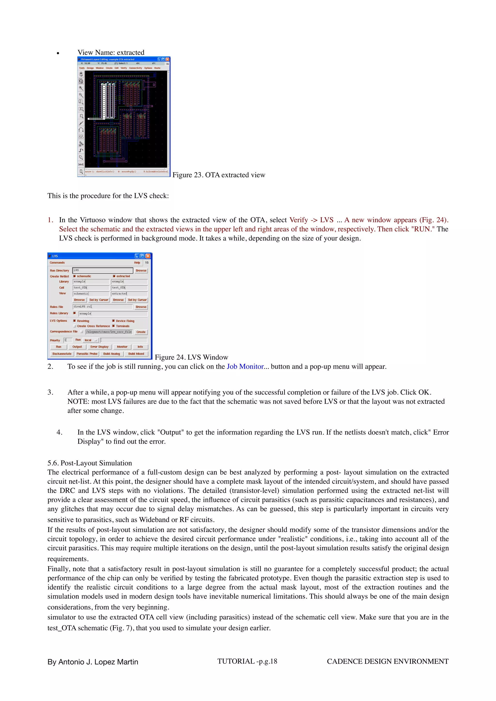
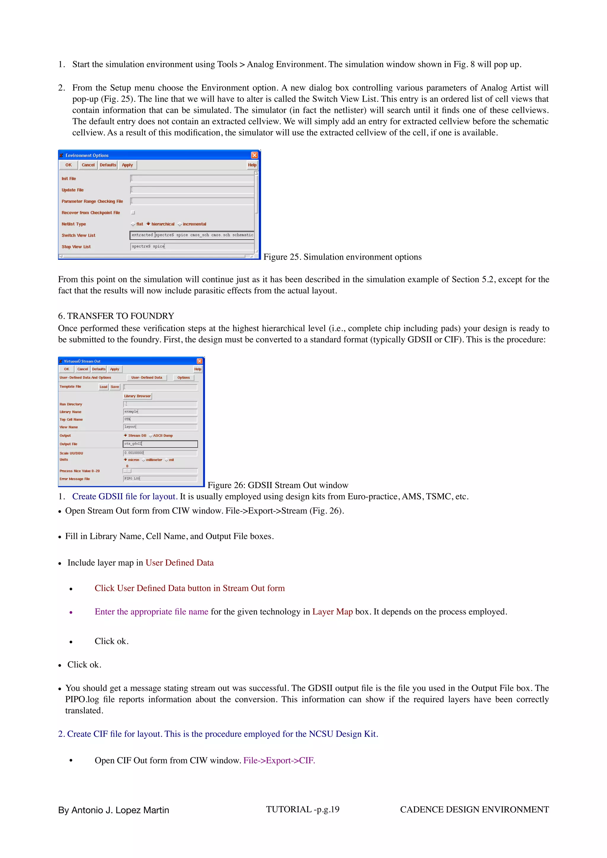
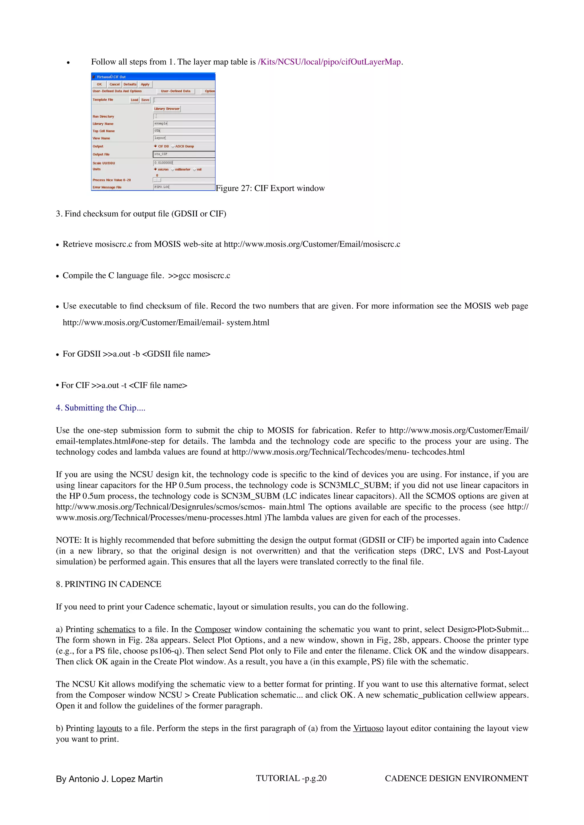
Unix is a family of operating systems derived from the original AT&T Unix developed in the 1970s at Bell Labs. Linux is an open source operating system based on the Linux kernel, which was created by Linus Torvalds in 1991. Xming and PuTTY are software tools used to enable graphical interfaces over remote connections between Windows PCs and Unix/Linux systems. Virtual Network Computing (VNC) is another graphical desktop sharing system that can be used instead of Xming and PuTTY.
Kernel Recipes 2014 - What I’m forgetting when designing a new userspace inte...Anne Nicolas
The document provides advice on properly designing a new interface between userspace and the kernel. It discusses using the correct data types that have fixed sizes across architectures, avoiding implicit padding, filling holes in data structures, placing the header in include/uapi/linux, and tools like pahole and Trinity that can help test the interface. It emphasizes that the ABI cannot change once exposed to userspace and recommends getting reviews from linux-kernel@vger.kernel.org or linux-api@vger.kernel.org mailing lists.
The document provides an overview of the initialization phase of the Linux kernel. It discusses how the kernel enables paging to transition from physical to virtual memory addresses. It then describes the various initialization functions that are called by start_kernel to initialize kernel features and architecture-specific code. Some key initialization tasks discussed include creating an identity page table, clearing BSS, and reserving BIOS memory.
The document provides an overview of Lab 1 for ECEN 474/704. The objectives are to learn Linux commands, Cadence basics, and MOS transistor characterization. Students will create an inverter schematic in Cadence, simulate it, and measure transistor model parameters like threshold voltage. The document reviews transistor operation and SPICE models. It provides instructions for starting Cadence, creating a library and cell, building an inverter schematic, setting up a DC simulation, and interpreting output plots.
This document summarizes the previous state of software development prior to .NET, including the use of punched cards, assembly programming, C/Windows API, C++/MFC, Visual Basic 6.0, Java, and COM. It then introduces the .NET framework as a solution that provides language interoperability, a common runtime, and base class libraries. Key aspects of .NET are discussed like the Common Language Specification, Common Type System, and Common Language Runtime. The session concludes by discussing potential criticisms of .NET and suggestions for further reading.
A Beowulf cluster is a computer cluster of what are normally identical, commodity-grade computers networked into a small local area network with libraries and programs installed which allow processing to be shared among them. The result is a high-performance parallel computing cluster from inexpensive personal computer hardware.
The name Beowulf originally referred to a specific computer built in 1994 by Thomas Sterling and Donald Becker at NASA.[1] The name "Beowulf" comes from the Old English epic poem of the same name.
No particular piece of software defines a cluster as a Beowulf. Beowulf clusters normally run a Unix-like operating system, such as BSD, Linux, or Solaris, normally built from free and open source software. Commonly used parallel processing libraries include Message Passing Interface (MPI) and Parallel Virtual Machine (PVM). Both of these permit the programmer to divide a task among a group of networked computers, and collect the results of processing. Examples of MPI software include Open M
The conversion of the ARM Linux kernel over to the Device Tree as the mechanism to describe the hardware has been a significant change for ARM kernel developers. Nowadays, all developers porting the Linux kernel on new ARM platforms, either new SOCs or new boards, have to work with the Device Tree. Based on practical examples, this talk intends to provide a ""getting started guide"" for newcomers in the Device Tree world: what is the Device Tree? How is it written and compiled? How do the bootloader and kernel interact? How are Device Tree bindings written and documented? What are the best practices for writing Device Trees and their bindings?
Video available at https://www.youtube.com/watch?v=m_NyYEBxfn8.
The document discusses the architecture of the Linux kernel. It describes the user space and kernel space components. In user space are the user applications, glibc library, and each process's virtual address space. In kernel space are the system call interface, architecture-independent kernel code, and architecture-dependent code. It then covers several kernel subsystems like process management, memory management, virtual file system, network stack, and device drivers.
This document provides an overview of embedded Linux. It defines embedded Linux as porting the Linux kernel to run on a specific CPU and board that will be placed in an embedded device. It discusses common embedded Linux distributions and components like bootloaders, kernels, and file systems. It also outlines the process for building an embedded Linux system, developing applications for it using common free tools, and emulating or testing on real hardware.
Making Clouds: Turning OpenNebula into a ProductNETWAYS
What does it takes to bring innovations like private clouds to small and medium enterprises? In the course of this talk we will present our experience in creating a self-service toolkit for creating a complete virtualization and cloud platform based on OpenNebula, as well as our experience gathered in tens of installations of all sizes. From scalable storage (with benchmarks!) to autonomic optimization, we will present what in our view is needed to bring private clouds to everyone, what components and additions we created to better solve our customers’ problems (from replacing industrial control systems to medium scale virtual desktop infrastructures), and why OpenNebula has been chosen over other competing cloud toolkits.
OpenNebulaConf 2013 - Making Clouds: Turning OpenNebula into a Product by Car...OpenNebula Project
What does it takes to bring innovations like private clouds to small and medium enterprises? In the course of this talk we will present our experience in creating a self-service toolkit for creating a complete virtualization and cloud platform based on OpenNebula, as well as our experience gathered in tens of installations of all sizes. From scalable storage (with benchmarks!) to autonomic optimization, we will present what in our view is needed to bring private clouds to everyone, what components and additions we created to better solve our customers’ problems (from replacing industrial control systems to medium scale virtual desktop infrastructures), and why OpenNebula has been chosen over other competing cloud toolkits.
Bio:
Carlo Daffara the Technical director of Cloudweavers, and formerly head of research and development at Conecta, a consulting firm specializing in open source systems and distributed computing; Italian member of the European Working Group on Libre Software and co-coordinator of the working group on SMEs of the EU ICT task force on competitiveness. Since 1999, works as evaluator for IST programme submissions in the field of component-based software engineering, GRIDs and international cooperation. Coordinator of the open source platforms technical area of the IEEE technical committee on scalable computing, co-chair of the SIENA EU cloud initiative roadmap editorial board and part of the editorial review board of the International Journal of Open Source Software & Processes (IJOSSP).
This document provides an overview of multimedia capabilities and libraries for embedded Linux systems, including DirectFB and SDL. It describes key multimedia concepts and gives brief descriptions of the main features and capabilities of DirectFB and SDL, including video playback, audio, input handling, and acceleration. It also discusses using these libraries for multimedia development on embedded Linux targets.
I have described all about linux OS starting from basics.
I guess this PPT will really be very very helpful for you guys.
This was one of the most appreciable PPT in my time when i presented it in my class.
This document discusses System on Chip (SoC) design and related topics. It provides an overview of SoC design, including definitions of SoC, typical architectures, challenges, and applications. It also summarizes System Generator, a tool for designing DSP applications on FPGAs, and DIP Lab software, which is used for image and video processing applications.
This document provides an overview and introduction to using the curses module in Python for writing text-based terminal applications. It describes initializing and terminating curses, creating windows and pads, displaying text with attributes and colors, and getting user input. The curses module hides complex terminal control codes and provides a consistent interface for building terminal applications that works across systems.
An embedded system is a microprocessor-based system designed to perform specific tasks and embedded as a component in a larger system. Common application areas include automotive electronics, aircraft electronics, trains, and telecommunications. The key design challenge is to optimize numerous design metrics like unit cost, size, performance, power consumption, and flexibility simultaneously. Common integrated circuit technologies used include full-custom/VLSI, semi-custom ASICs, and programmable logic devices like FPGAs. VHDL and Verilog are hardware description languages used to model and simulate the system at different levels of abstraction from transistors to functional behavior.
First Steps Developing Embedded Applications using Heterogeneous Multi-core P...Toradex
Read our blog for the latest on demystifying the development of embedded systems using Heterogeneous Multicore Processing architecture powered SoCs! This might provide you with the jump start you need for your development. https://www.toradex.com/blog/first-steps-developing-embedded-applications-using-heterogeneous-multicore-processors
Introduction to embedded linux device driver and firmwaredefinecareer
This document provides an introduction to embedded Linux and device drivers. It defines an embedded system as a special-purpose computer designed to perform dedicated functions with real-time constraints, often embedded as part of a complete device. Linux is commonly used in embedded systems due to advantages like reuse of existing components, community support, and low cost. The document outlines the typical hardware and software requirements for developing embedded Linux systems, and provides an overview of the Linux kernel architecture for device drivers, including the unified device model, bus drivers, and platform devices.
The document provides information about accessing Linux from Windows using SSH. It discusses using programs like Putty, Xming, MobaXterm, and SmarTTY to connect to a Linux server. These programs allow running both command line and graphical applications remotely. The document also covers basic Linux commands like cal, ncal, echo, and tput to display calendars, output text, and query the terminal database for features.
The document discusses Microsoft's .NET framework. It defines .NET as a new platform for developing and running software applications that features ease of development of web services and interoperability between programming languages. It then goes on to describe key concepts in .NET including the Common Language Runtime (CLR), assemblies, application domains, garbage collection, and serialization.
The Raspberry Pi is a series of credit card–sized single-board computers developed in the UK by the Raspberry Pi Foundation with the intention of promoting the teaching of basic computer science in schools.
The original Raspberry Pi and Raspberry Pi 2 are manufactured in several board configurations through licensed manufacturing agreements with Newark element14 (Premier Farnell), RS Components and Egoman. These companies sell the Raspberry Pi online. Egoman produces a version for distribution solely in China and Taiwan, which can be distinguished from other Pis by their red colouring and lack of FCC/CE marks. The hardware is the same across all manufacturers.
The original Raspberry Pi is based on the Broadcom BCM2835 system on a chip (SoC), which includes an ARM1176JZF-S 700 MHz processor, VideoCore IV GPU, and was originally shipped with 256 megabytes of RAM, later upgraded (models B and B+) to 512 MB. The system has Secure Digital (SD) (models A and B) or MicroSD (models A+ and B+) sockets for boot media and persistent storage.
This slideshow gives feedback about using Linux in industrial projects. It is part of a conference held by our company CIO Informatique Industrielle at ERTS 2008, the European Embedded Real Time software Congress in Toulouse
Ansible is an automation tool that allows users to deploy applications, manage systems, and simplify complexity through automation without using scripts or custom code. It leverages SSH and requires no agents to be installed on remote systems. Ansible describes infrastructure in a language that is both machine- and human-friendly and allows users to instantly manage new remote machines without bootstrapping. Playbooks can be used to describe deployment and configuration policies across multiple systems.
The document discusses cross-compiling native packages for Android using autotools or cmake. It describes downloading and configuring the Android NDK, which provides cross-compilation tools for ARM, x86, and MIPS architectures. It then gives steps to cross-compile the expat library as an example, including downloading the sources, extracting them, and configuring/building using the autotools system. Key points covered include limitations of the Bionic C library used on Android and associations between Android API levels and supported architectures.
Symica is an electronic design automation tool for analog and mixed-signal integrated circuit design. It supports hierarchical design entry and compatibility with popular simulation models. Symica has capabilities for modern IC development including accommodating different process design kits. Its affordable and flexible pricing makes it attractive for startups and independent researchers. Established semiconductor companies can use Symica as a cost-saving solution for expanding design capabilities beyond limited licenses from major EDA vendors.
Gene's law, Common gate, kernel Principal Component Analysis, ASIC Physical Design Post-Layout Verification, TSMC180nm, 0.13um IBM CMOS technology, Cadence Virtuoso, FPAA, in Spanish, Bruun E,
The Tektronix MDO3104 is a mixed domain oscilloscope with 1 GHz analog bandwidth and built-in spectrum analyzer, arbitrary function generator, logic analyzer, and protocol analyzer. It offers 4 analog channels, 16 digital channels, and 1 RF input channel. The MDO3104 also supports a variety of serial protocols and comes with various optional application modules for extended analysis capabilities.
Low power sar ad cs presented by pieter harpeHoopeer Hoopeer
The document discusses the operation and design tradeoffs of SAR and sigma-delta analog-to-digital converters (ADCs). It explains that SAR ADCs use a binary search approach to determine each output bit but are limited by noise and nonlinearity issues from components like track-and-hold switches and digital-to-analog converters. Sigma-delta ADCs shift quantization noise out of band through oversampling and noise shaping to achieve high resolution without requiring high-precision analog components. The document also covers speed limitations of SAR ADCs and how power consumption scales with resolution for different blocks like comparators and logic.
Lab 2: Cadence Tutorial on Layout and DRC/LVS/PEX
This section describes how to extract a netlist from your layout that includes parasitic resistances and capacitances. You will then be able to re-simulate your design with extracted parasitics in Spectre. PEX requires a clean LVS so that extracted parasitics can be correlated to nets on the schematic. Initiate the PEX interface by clicking on:Calibre > Run PEX
A window asking to load a runset file will now appear. Browse to the file
Step by step process of uploading presentation videos Hoopeer Hoopeer
Deep neural network, compressive sensing, floating gate techniques can be efficiently employed to increase voltage swing and reduce supply voltage requirements of class AB regulated cascode current mirrors, implement extreme low power analog circuits with this process. /also have good references for subthreshold region.
[Extreme Low Power Differential Pair: An Experimental Evaluation, Super-Gain-Boosted Miller Op-Amp based on Nested Regulated Cascode Techniques , Step by Step process of uploading presentation videos, Dennis Ritchie The creator of the C programming language and co-creator of Unix
This document is a project report submitted by Renu Gupta to fulfill requirements for a Master's degree in Electronics and Communication Engineering. The project involves realizing various signal processing and generating circuits using an Operational Trans-Resistance Amplifier (OTRA). The OTRA is implemented using commercially available CFOA ICs. Circuits designed include filters, oscillators, and an active inductor-based LC oscillator. Theoretical results are verified through PSPICE simulations and experiments using practical circuits assembled with CFOA ICs. The report documents the work conducted under the guidance of Dr. Neeta Pandey.
S-parameters are used to analyze microwave circuits operating between 300MHz to 1000GHz. S-parameters relate the input and output traveling wave variables of network components using a scattering matrix. For a two-port network, the S-parameters relate the incident and reflected waves at each port. S11 and S22 represent reflection coefficients, while S12 and S21 represent transmission coefficients. Networks can be reciprocal if S12 = S21, and symmetrical if S11 = S22. LTSpice can be used to simulate S-parameters for two-port networks.
Influential and powerful professional electrical and electronics engineering ...Hoopeer Hoopeer
powerful professional electrical and electronics engineering books
. Analysis and Design of Analog Integrated Circuits
Analysis and Design of Analog Integrated Circuits
Analog filter design
This document provides instructions for assembling and operating a 3-stage FM transmitter kit. It includes a list of components, descriptions of each circuit stage including amplification, oscillation and tuning, and guidance on assembling, powering and tuning the transmitter to broadcast within the FM radio band. The transmitter is designed to transmit audio from a microphone up to 1 km when powered by a 9V battery and connected to an antenna.
The Teager Energy Operator (TEO) is a feature extraction circuit used for electroencephalography (EEG) signals. TEO uses a low-pass filter and multiplier to measure instantaneous energy, which can help classify specific sleep stages. TEO is designed using a mathematical formula and extracts features from EEG signals by measuring energy. It is one tool among others, including signal level detection and peak detection, that can extract features from EEG, electromyography, and electrooculography signals.
The document provides information about the Department of Physics at the University of Patras in Greece. It includes details such as the chairperson, degrees offered, faculty members, laboratories, courses, and research activities. The department has over 1200 undergraduate students and 70 graduate students. There are 50 faculty members across four divisions conducting teaching and research in various fields of physics.
The document provides 15 links to YouTube videos and one link to a PDF file featuring lectures on various topics. The YouTube videos range in length from 15 minutes to over an hour and cover subjects such as Islamic theology, philosophy and spirituality. The linked PDF file is a condensed nightly prayer handbook.
1. The document provides instructions on how to generate a layout view in Cadence Virtuoso and perform layout verification and simulation with extracted parasitics. It describes creating a CMOS inverter layout including placing nFET and pFET devices and connecting their terminals.
2. Key layers used in the layout are described, including Metal 1 (M1), Poly (PC), Diffusion (RX), Contact (CA), N-well (NW), P+ implant (BP), and Via 1 (V1). Design rules for spacing and dimensions are outlined.
3. An example inverter layout is shown, and instructions are provided on how to move and edit devices, enter layout shapes, and connect the devices to
The document discusses various performance evaluation metrics that are commonly used to evaluate classification algorithms and predictive models, including accuracy, precision, recall, F1 score, confusion matrix, receiver operating characteristic curve, and precision-recall curve. It provides definitions and formulas for calculating each of these metrics and discusses their strengths and weaknesses for evaluating model performance, especially for imbalanced datasets. Examples of each metric are given from literature on applications like seizure detection, trust prediction in social networks, and gene association networks. Feature extraction techniques for biomedical signals like EEG are also mentioned.
BJT and MOS, Advanced Circuit Topologies, concept of tracking, mm-Wave frequency beyond 30GHz, Bandgap is a stable, well defined, and constant current source
This document provides an overview of VLSI-compatible implementations for artificial neural networks. It begins with an introduction and motivation for the work. The objectives are to develop generalized artificial neural network models and architectures that can be implemented using standard VLSI technologies. Various hardware implementation techniques for neural networks are reviewed, including pulse-coded, digital, and analog approaches. Different analog implementations like resistive synaptic weights, switched capacitor neurons, current-mode and sub-threshold designs are discussed. The document concludes with a comparison of some existing neural network hardware systems and a summary of the chapter.
William Strange earned his PhD in 1959 from the University of California, Los Angeles under advisor Peter Henrici. His thesis was titled "Difference Methods for Mixed Boundary Value Problems". One of his PhD students was Hermann Flaschka.
Applications of artificial Intelligence in Mechanical Engineering.pdfAtif Razi
Historically, mechanical engineering has relied heavily on human expertise and empirical methods to solve complex problems. With the introduction of computer-aided design (CAD) and finite element analysis (FEA), the field took its first steps towards digitization. These tools allowed engineers to simulate and analyze mechanical systems with greater accuracy and efficiency. However, the sheer volume of data generated by modern engineering systems and the increasing complexity of these systems have necessitated more advanced analytical tools, paving the way for AI.
AI offers the capability to process vast amounts of data, identify patterns, and make predictions with a level of speed and accuracy unattainable by traditional methods. This has profound implications for mechanical engineering, enabling more efficient design processes, predictive maintenance strategies, and optimized manufacturing operations. AI-driven tools can learn from historical data, adapt to new information, and continuously improve their performance, making them invaluable in tackling the multifaceted challenges of modern mechanical engineering.
Software Engineering and Project Management - Introduction, Modeling Concepts...Prakhyath Rai
Introduction, Modeling Concepts and Class Modeling: What is Object orientation? What is OO development? OO Themes; Evidence for usefulness of OO development; OO modeling history. Modeling
as Design technique: Modeling, abstraction, The Three models. Class Modeling: Object and Class Concept, Link and associations concepts, Generalization and Inheritance, A sample class model, Navigation of class models, and UML diagrams
Building the Analysis Models: Requirement Analysis, Analysis Model Approaches, Data modeling Concepts, Object Oriented Analysis, Scenario-Based Modeling, Flow-Oriented Modeling, class Based Modeling, Creating a Behavioral Model.
Discover the latest insights on Data Driven Maintenance with our comprehensive webinar presentation. Learn about traditional maintenance challenges, the right approach to utilizing data, and the benefits of adopting a Data Driven Maintenance strategy. Explore real-world examples, industry best practices, and innovative solutions like FMECA and the D3M model. This presentation, led by expert Jules Oudmans, is essential for asset owners looking to optimize their maintenance processes and leverage digital technologies for improved efficiency and performance. Download now to stay ahead in the evolving maintenance landscape.
Introduction- e - waste – definition - sources of e-waste– hazardous substances in e-waste - effects of e-waste on environment and human health- need for e-waste management– e-waste handling rules - waste minimization techniques for managing e-waste – recycling of e-waste - disposal treatment methods of e- waste – mechanism of extraction of precious metal from leaching solution-global Scenario of E-waste – E-waste in India- case studies.
Batteries -Introduction – Types of Batteries – discharging and charging of battery - characteristics of battery –battery rating- various tests on battery- – Primary battery: silver button cell- Secondary battery :Ni-Cd battery-modern battery: lithium ion battery-maintenance of batteries-choices of batteries for electric vehicle applications.
Fuel Cells: Introduction- importance and classification of fuel cells - description, principle, components, applications of fuel cells: H2-O2 fuel cell, alkaline fuel cell, molten carbonate fuel cell and direct methanol fuel cells.
Data Control Language.pptx Data Control Language.pptx
Cadence design environment
1. Unix is a family of multitasking, multiuser computer operating systems that derive from the original AT&T Unix, development
starting in the 1970s at the Bell Labs research center by Ken Thompson, Dennis Ritchie, and others.
Unix commands are case sensitive.
Linux is a family of open source Unix-like operating systems based on the Linux kernel, an operating system kernel first released on
September 17, 1991, by Linus Torvalds. Linux is typically packaged in a Linux distribution.
Linux is an operating system that is a multi-user, multi-tasking system that can be used on servers, desktops and laptops. Linux was
originally developed at Bell Labs in 1969. Linux is used to access cadence and manage the files in its libraries.
The X Window System is a windowing system for bitmap displays, common on Unix-like operating systems. X provides the basic
framework for a GUI environment: drawing and moving windows on the display device and interacting with a mouse and keyboard.
Xming is an X11 display server for Microsoft Windows operating systems, including Windows XP and later
PuTTY is a free and open-source terminal emulator, serial console and network file transfer application. It supports several network
protocols, including SCP, SSH (secure shell (SSH)), Telnet, rlogin, and raw socket connection. It can also connect to a serial port.
The name "PuTTY" has no official meaning.
http://laptops.eng.uci.edu/software-installation/using-linux/how-to-configure-xming-putty?
tmpl=%2Fsystem%2Fapp%2Ftemplates%2Fprint%2F&showPrintDialog=1
https://www.egr.msu.edu/classes/ece410/mason/files/guide-410-setup-PC.pdf
By Antonio J. Lopez Martin TUTORIAL -p.g.1 CADENCE DESIGN ENVIRONMENT
2. Xming software is a graphic server that runs on the PC to supply remote login to the Xwindow system. PuTTy software is used to
setup a link between a remote Xwindow server (in UNIX or Linux) and the client PC. For programs that need a graphics interface,
Xming will help display this interface at client side.
X Windows servers like Exceed, X-Win32, or Xfree (Linux).
More recent, X2Go enables users to access a graphical desktop of a Linux computer over a network connection. The use of X2Go
allows the ability to disconnect and resume sessions, even from another client.
Note: This replaces ssh and Xming with one software package and allows sessions to be suspended and resumed later. Only one
session is allowed per machine. For all other servers, you will need to use your preferred SSH client and launch applications via the
command-line interface.
(Xfree old), (Xming new: used).
Instead of PuTTY and Xming, MobaXterm.
For all applications requiring graphical display (Cadence or Matlab) on a remote machine, ssh -X, putty +Xming, or VNC
Also the VNC software can be employed (see the accompanying document about VNC tools).
In computing, Virtual Network Computing (VNC) is a graphical desktop-sharing system that uses the Remote Frame Buffer
protocol (RFB) to remotely control another computer. It transmits the keyboard and mouse events from one computer to another,
relaying the graphical-screen updates back in the other direction, over a network.
VPN for off-campus
https://www.google.com/url?
sa=t&rct=j&q=&esrc=s&source=web&cd=&cad=rja&uact=8&ved=2ahUKEwjoxajM2PvpAhVFrxoKHeHgAqA4ChAWMAd6BAg
JEAE&url=https%3A%2F%2Fucirvine.instructure.com%2Ffiles%2F1604071%2Fdownload%3Fdownload_frd%3D1&usg=AOvVa
w2or9Y7X6sKmJTKOY6jkRs9
Note: OS X systems (10.7 & above) will need to install XQuartz
(link is external)
to enable X-Windows sessions. X-Windows is no longer supported natively.
Cadence main window (Common Interface Window, CIW) and Library Manager Window
CIW menus, all Cadence main tools, online help and options can be accessed.
http://www.accessam.com/myip.shtml
In the window area, all kind of messages (info, errors, warnings, etc) generated by the different Cadence tools appear. You can also
introduce commands
CIW window
All the entities in Cadence are managed using libraries and each library contains cell. Each cell contains difference design views. (the
structure is similar –and physically corresponds - to a directory (library) containing subdirectories (cells), each one containing files
(views). Thus, for instance, a certain circuit (e.g. an ADC) can be stored in a library, and such library can contain the different ADC
blocks (comparators, registers, resistor strings, etc) stored as cells. Each block (cell) contains different views (schematic, layout, etc.).
There are usually three types of libraries:
By Antonio J. Lopez Martin TUTORIAL -p.g.2 CADENCE DESIGN ENVIRONMENT
3. • A set of common Cadence libraries that come with the Cadence software (containing basic components, such as voltage
and current sources, R, L, C, etc).
• Libraries that come with a certain design kit and that are related to a certain technology (e.g. transistors with a certain
model attached, etc). In the NCSU design kit, some general Cadence libraries are customized and converted into design kit
libraries.
• User libraries; where the user stores its designs. These designs employ components from the Cadence/design kit libraries.
All the libraries are managed from the Library Manager Window.
This kit can be freely obtained from the North Carolina State University
Tools>Library Manager... from the CIW. Libraries with names starting by NCSU are design kit libraries and contain basic
components for building designs
* NCSU_Analog_Parts: contains all the required blocks for designing an analog schematic (sources, GND and VDD terminals,
transistors, R, L, C, diodes, etc.)
* NCSU_Digital_Parts: similarly, it contains all parts required for digital design (logic gates, muxes, etc.)
* NCSU_Sheets_8ths: it contains informative sheet borders for the schematics, in different sheet sizes. Its use is optional, for design
documentation.
* NCSU_TechLibAMI06: it is a technology-specific library that is created when the user attaches this particular technology
(AMI06) to a user library.
Library Manager window
It is recommended that you use a library to store related cell views; e.g., use a library to hold all the cell views for a single project
(that can involve a complete chip design).
Create a new library for our design. From the CIW or from the Library Manager window:
• a) Select File -> New -> Library. A new window appears (see Fig. 4).
• b) Enter a library name, e.g., example.
• c) Enter the absolute path name if you want the library created somewhere else than the working
directory.
• d) Choose the Attach to an existing techfile option.
• e) Choose your technology; for instance, for AMI 0.5μm in MOSIS, choose AMI 0.6u C5N
Create Library window
By Antonio J. Lopez Martin TUTORIAL -p.g.3 CADENCE DESIGN ENVIRONMENT
4. 1/Schematic Entry with Composer
From the CIW or from the Library Manager window,
a) Select the library name that you just created, e.g., example.
b) Select File -> New -> Cellview
c) Enter a cell name, for instance, OTA
d) Choose Composer - Schematic as the Tool. View name should be schematic. e)
Click OK.
NOTE: There are three-terminal (nmos, pmos) and four-terminal (nmos4, pmos4) MOS devices available. The three-terminal devices
have a hidden fourth (bulk) terminal, which is connected by default to "gnd!" for nmos and "vdd!" for pmos. This means that you
need to have nets named "vdd!"and "gnd!" somewhere in your schematic. (The easiest way to do this is to drop in the vdd and gnd
pins from NCSU_Analog_Parts->Supply_Nets.) If you don't have these nets in your schematic somewhere, you'll get complaints
about unknown nets either in the netlister or in LVS. (You can also change the bulk node in the three-terminal device if you want to.
Just select the device in the schematic, and bring up the "Edit Object Properties" form (Edit->Object- >Properties...). Change the
"Bulk node connection" field to whichever net you want.
-set instance properties: you can modify at any time the properties of a certain component instance (resistance value, transistor
dimensions, etc), e.g., by selecting the instance (click on it) and then clicking on the Properties icon. You can also change a group of
instances of the same component simultaneously, by first selecting this group, then clicking in Properties and modifying the
parameters, selecting Apply to > All selected.
-There are basically two ways of creating schematics:
a) Non-Hierarchical schematic. You introduce all the circuit schematic at the same (transistor) level, including the required sources.
This is only viable for small designs.
b) Hierarchical schematic. If your design is very large, or if you want to reuse your design in other designs (e.g. an OpAmp to be
employed in other circuits), you should create basic blocks at a low level, then create symbols for them and then use these symbols as
basic components at a higher hierarchical level of the design. It is the same concept employed in SPICE netlists with the .SUBCKT
command.
-Symbol Creation
• First, you have to create pins in your schematic in those non-global nets (inputs, outputs, supplies perhaps) that have to be accessible outside the symbol. For
doing this, you can select the Create Pin icon in the Composer schematic window, select the pin name, its input or output configuration, etc, and then click at
the end of the wire when the pin has to be placed. Six pin icons have been placed in the example of Fig. 5: v+, v-, ibias, vdd, vss (input pins) and out (output
pin).
• Now, select Design > Create Cellview > From cellview. A window appears that by default creates a symbol view from the schematic view. Just click OK. A
black window pops up with the symbol. It can be edited if desired (changing shape, pin distribution, etc.). Fig. 6 shows the resulting symbol (after some
editing) and the actions associated to the left icons.
Symbol Editor window
By Antonio J. Lopez Martin TUTORIAL -p.g.4 CADENCE DESIGN ENVIRONMENT
5. Composer Schematic Editor window, hierarchical design
2/Simulation
The initial simulation phase also serves to detect some of the design errors that may have been created during the schematic entry
step. It is quite common to discover errors such as a missing connection or an unintended crossing of two signals in the schematic.
Some of these errors (e.g., floating nodes) can be detected even before simulation, by pressing the Check and Save icon in the
schematic window.
The second simulation phase will follow the "extraction" of a mask layout (post-layout simulation), to accurately assess the electrical
performance of the completed design. Like in other simulation environments, it is the netlist text file extracted from the schematic (or
layout) what is actually simulated.
In order to start simulations, from the Composer window that contains the schematic you want to simulate (in our example,
test_OTA, shown in Fig. 7), choose Tools > Analog Environment. The simulation window appears (Fig. 8).
Simulation window
By default, the design from which we have launched the window can be simulated using Spectre.
Setting simulator
We can change the design with the corresponding icon or using the menus. We can also change the simulator (from Spectre to
another simulator) by choosing Setup->Simulator/Directory/Host and setting e.g., HSPICE. Obviously, the chosen simulator must be
installed and licensed.
Setting models
Also by default the component models for the library technology (in our example AMI 0.5μ) will be used. If we want to use other
models, we can store them in some directory and choose Setup- >Model Path, typing the full path (including filename) of the
model(s) needed for simulation, before the path for the default models (list position means precedence in the search for models). This
procedure assumes that your models have the same name as the default models.
Setting design variables
We can use in our schematic design variables for the component parameters, so that their values can be assigned just before
simulation. For instance, we can name some (or all) of the transistor lengths as ‘L’. Then, in the simulation window we assign the
desired value to L. This way, we can make several simulations just changing the parameter(s) without having to edit the schematic.
For editing design variables, choose Variables >Edit (or select the corresponding icon).
Selecting the analysis
By Antonio J. Lopez Martin TUTORIAL -p.g.5 CADENCE DESIGN ENVIRONMENT
6. Several analyses can be performed (DC, AC, transient, etc.). For selecting the required analysis, choose Analysis > Choose (or the
corresponding icon) and complete the settings in the window that appears. Example: Transient analysis, choose 'tran', ‘conservative’
and then type in the total time you wish to run (ex. 40n or 40e-9). Currents cannot be plotted by default. If you are interested in
viewing currents in your circuit, choose: Output > Save all ....> Select all DC/transient terminal currents (for DC and transient
analyses) or Select all AC terminal currents (for AC analysis).
Running the simulation
When the former steps are performed, simulation can start. Click the Green Traffic Light Icon (bottom right corner of the simulation
window) or choose Run > Simulation to run the simulation. If you want to interrupt the simulation at any instant, click the Red
Traffic Light Icon or choose Run > Interrupt.
Plotting the simulation results
There are different ways of plotting the results of a simulation. Here we are going to use the Calculator tool. After running the
simulation, choose Tools > Calculator. A calculator window appears (see Fig. 9).
Figure 9. Calculator
With this tool we can, among other things:
• Plot in a waveform window the different currents and voltages
• Print (to a printer or a file) the selected waveforms
• Perform different functions on the selected waveform (multiply, divide, dB calculation, DFT, THD calculation, bandwidth,
maximum and minimum calculation, etc).
• Use as a normal calculator for making calculations. You can select the Help option for details.
When we want to display a certain waveform, we first select the button corresponding to the type of waveform. The most
common are:
- Vt: nodal voltage (transient analysis) It: terminal current (transient analysis) Vf: nodal voltage (AC analysis)
- If: terminal current (AC analysis)
- Vs: nodal voltage (DC sweep)
- Is: terminal current (DC sweep)
- Vdc: nodal voltage (quiescent value)
- Idc: terminal current (quiescent value)
Then, we just click on the corresponding wire (voltages) or terminal (currents) in the schematic. Finally, we select in the calculator:
Plot: To plot the waveform without removing already displayed waveforms
Erplot: To remove displayed waveforms and plot the selected one.
The waveform is plotted in the Waveform Window. We can continue selecting circuit nodes and selecting plot or erplot. Finally, press
Esc for disabling the current action.
The Waveform Window, showing the input and output voltages of our voltage buffer, is shown in Fig. 10. Different configurations
can be chosen (various graphs or axes, cursors, etc.). Press the Help button for details.
If you want to modify and re-simulate your circuit, just change your schematic, design variables or simulation command, run again
the simulation and select Window > Update results in the Waveform Window.
By Antonio J. Lopez Martin TUTORIAL -p.g.6 CADENCE DESIGN ENVIRONMENT
7. Waveform window
3/Layout
The creation of the mask layout is one of the most important steps in the full-custom (bottom-up) design flow, where the designer
describes the detailed geometry and the relative positioning of each mask layer to be used in actual fabrication, using a Layout Editor.
Physical layout design is very tightly linked to overall circuit performance (area, speed and power dissipation) since the physical
structure determines the transconductances of the transistors, the parasitic capacitances and resistances, and obviously, the silicon
area that is used to realize a certain function.
The physical (mask layout) design is an iterative process, which starts with the circuit topology and the initial sizing of the
transistors. It is extremely important that the layout design must not violate any of the Layout Design Rules of the fabrication
process, in order to ensure a high probability of defect-free fabrication of all features described in the mask layout. It is also
important to Extract the netlist underlying the layout view, for two main purposes:
• This allows comparing it with the netlist extracted from the schematic. This Layout versus Schematic (LVS) comparison
ensures that the layout actually implements the required functionality.
• If the extraction program allows to extract also parasitics from the layout view, a more accurate, Post-Layout Simulation,
can be performed taking into account the geometry of the circuit.
The detailed mask layout requires a very intensive and time-consuming design effort, so that automated tools are employed as much
as possible. Typically, the design of digital circuits based on single-clock synchronous logic is completely automated. First, a circuit
description (typically in a HDL language as VHDL or Verilog) is synthesized, leading to a gate-level circuit description. From this
gate-level netlist, Place&Route programs generate automatically the layout.
Unfortunately, analog circuits are very sensitive to the layout style, so that an automated procedure is difficult to implement.
Usually a tedious, full-custom approach is followed, where the designer builds manually the layout, basically drawing rectangles of
different layers. Nevertheless, there are some aids to the full-custom designer:
• Parametrized Cells (Pcells). They are complete layout cells (e.g. a transistor or a row of contacts) already available, containing all
the required layers, and whose characteristics can be set by the designer by means of some parameters (e.g., transistor length or
width, etc.). They can be implemented in Cadence using the SKILL language, and some of them come usually with a certain
Design Kit.
• Standard Cells. Cells already designed that can be placed in our layout. In case of digital cells, they are usually automatically
placed with a Place&Route program. The availability of parametrized and standard cells in a certain Design Kit is an important
factor for its quality (and price!).
• “Semi-automated” layout. The layout of the components in the schematic is automatically generated from the schematic, with its
corresponding sizes. The designer just places and routes such components. Even for assisting place and route tasks there are
additional features available. This can be done in Cadence with the Virtuoso Accelerator (Virtuoso XL).
We will now make the layout of our OTA. From the CIW or from the Library Manager window,
a) Select the library name that you just created, e.g., example.
b) Select File -> New -> Cellview
By Antonio J. Lopez Martin TUTORIAL -p.g.7 CADENCE DESIGN ENVIRONMENT
8. c) Enter the cell name, e.g., OTA
d) Choose Virtuoso as the Tool. View name should be layout.
f) Click OK. Two design windows will pop up (see Fig. 11), LSW and Virtuoso Editor.
LSW
Virtuoso and LSW windows
The Layer Selection Window (LSW) lets the user select different layers of the mask layout. Virtuoso will always use the layer
currently selected in the LSW for editing. The LSW can also be used to restrict the type of layers that are visible or selectable. To
select a layer, simply click on the desired layer within the LSW.
WARNING: Only layers with the dg property will be fabricated. The rest are basically for labeling, highlighting errors, and
documenting!!
• Common Layers. The following layers are common to all MOSIS CMOS processes:
Table I. Common layers in all MOSIS processes
• Layers corresponding to optional technology features. Some specific additional layers can be included for implementing optional
features of the technology. Table II shows which active processes support which optional technology features. Table III shows the
mask layers that correspond to the technology features.
By Antonio J. Lopez Martin TUTORIAL -p.g.8 CADENCE DESIGN ENVIRONMENT
9. Table III. Additional layers supporting the optional features
Virtuoso
Virtuoso is the main layout editor of Cadence design tools. There is a small (icon) button bar on the left side of the editor. Commonly
used functions can be accessed pressing these buttons. There is an information line at the top of the window. This information line,
(from left to right) contains the X and Y coordinates of the cursor, number of selected objects, the traveled distance in X and Y, the
total distance and the command currently in use. This information can be very handy while editing. At the bottom of the window,
another line shows what function the mouse buttons have at any given moment. Note that these functions will change according to
the command you are currently executing.
“Basic” Full-Custom layout (Process)
The layout is made layer by layer, in any order. This is similar to the mask layout edition in Magic or L-Edit. In Cadence, this is not
usually done in practice (unless the Layout Editor/Design Kit do not support more advanced methods). This is included here as a
reference, you can skip this section and go to the more practical approaches of Sections 5.3.2 and 5.3.3.
In our example the technology selected is n-well, so that the black area represents the p substrate. The full custom layout process
consist basically on repeatedly selecting a certain layer from the LSW window, choosing the Rectangle icon to create a rectangle and
drawing it.
As mentioned above, the geometries (enclosure, extension, minimum dimensions, etc) of the objects created have to comply with a
set of rules dependent on the technology, named Design Rules. Once your layout completed, a Design Rule Check (DRC) is
performed to enforce this point. Object dimensions can be checked by observing the screen coordinates or using the ruler (Ruler icon
or k shortkey).
-For designing a PMOS transistor of aspect ratio W/L (the order of layer drawing is irrelevant):
Since we are using an n-well process, the substrate will be p-substrate. To create a PMOS transistor we need an n-well in which the
transistor will be formed.
• Draw the well
-a) Select the n-well layer from the LSW window
-b) Select the Create->Rectangle (or choose the Rectangle icon from the side toolbar).
-c) Using your mouse, draw the n-well with the size required
• Draw the p- and n-select regions for the p transistor
-Select the pselect layer from the LSW window; we will draw the pselect enclosing the transistor
-Select the Create->Rectangle (or choose the Rectangle icon from the side toolbar).
-Using your mouse, draw the pselect on the cellview. The pselect should be placed within the n-well (you can use the Edit->Move
command to move the layer) with geometry according to the Design Rules.
• Draw Diffusions
-Select the pactive layer from the LSW window; we will draw the active region of the p-device
-Select the Create->Rectangle (or choose the Rectangle icon from the side toolbar).
By Antonio J. Lopez Martin TUTORIAL -p.g.9 CADENCE DESIGN ENVIRONMENT
10. -Using your mouse, draw the pactive on the cellview (it should be enclosed by the pselect and by the nwell, as determined by the
Design Rules). Its width should be W, and its length as small as possible, for reducing device parasitics.
—NOTE: In many SCMOS (standard CMOS) processes there are 3 active layers: active, nactive and pactive. They are
interchangeable since they translate to the same physical layer in fabrication. As mentioned in Table I, nactive and pactive layers are
provided for differentiating graphically n and p active diffusions (assigning them different colors) but what makes an active layer of
type n or p is the nselect or pselect layer, respectively, surrounding it).
• Draw Poly
a) Select the poly layer from the LSW window
b) Select the Create->Rectangle (or choose the Rectangle icon from the side toolbar).
c) Using your mouse, draw the poly on the cellview
The poly should be placed at the center of the p-island, with length L, and should extend over the p-island as specified in the Design
Rules.
• Place Contacts
a) Select the contact layer from the LSW window
b) Select the Create->Rectangle (or choose the Rectangle icon from
the side toolbar).
c) Using your mouse, draw the contact on the cellview. Most technologies require one (or two) fixed contact size/s.
Contacts should be placed at both sides of the pactive. You can copy the generated contact throughout the drain and source areas. The
number of contacts should be as large as possible. Their size is determined by the corresponding Design Rules.
- For designing a NMOS transistor of dimensions W/L (the order of layer drawing is irrelevant):
• Draw the nselect
-Select the nselect layer from the LSW window
-Select the Create->Rectangle (or choose the Rectangle icon from the side toolbar).
-Using your mouse, draw the nselect on the cellview
• Draw the N active region
-Select the nactive layer from the LSW window
-Select the Create->Rectangle (or choose the Rectangle icon from the side toolbar).
-Using your mouse, draw the nactive on the cellview ; it should be enclosed by the nselect (as determined by the Design Rules). Its
width should be W, and its length as small as possible.
• Draw Poly
-Select the poly layer from the LSW window
-Select the Create->Rectangle (or choose the Rectangle icon from the side toolbar).
-Using your mouse, draw the poly on the cellview. The poly should be placed at the center of the n-island, with length L, and should
extend over the n-island as specified in the Design Rules.
• Place Contacts
-Select the contact layer from the LSW window
-Select the Create->Rectangle (or choose the Rectangle icon from the side toolbar).
-Using your mouse, draw the contact on the cellview. Most technologies require one (or two) fixed contact size/s. Contacts should be
placed at both sides of the nactive. You can copy the generated contact throughout the drain and source areas. The number of contacts
should be as large as possible. Their size is provided by the corresponding Design Rules.
• Designing resistors:
Integrated resistors can be made by different layers (diffusion, well, poly). In analog applications linear resistors are usually
required, so that they are typically implemented using poly, and if technology allows, using a special high resistive poly layer.
The procedure for designing a resistor is as follows:
a) Determine the number of squares required by the resistor geometry:
No. squares =
Resistor Value(Ω)/Sheet Resistance(Ω / square)
Typical sheet resistances are 20-30 Ω/︎square for (silicide) poly and about 1 kΩ/︎square for the high-resistive poly.
(silicide: a binary compound of silicon with another element or group).
b) Choose the width W of the resistor strip. It should be larger than the minimum given by the Design Rules for fabricating resistors.
c) Obtain the length L of the resistor strip: L= W x No. Squares.
d) If L is too long, several bends can be introduced (thus forming serpentine resistors). Recalculate (b) counting about 1⁄2 square for
each bend corner. (serpentine: winding and twisting like a snake).
-Poly1 resistor
• Draw Poly
a) Select the poly layer from the LSW window
b) Select the Create->Rectangle (or choose the Rectangle icon from the side toolbar).
c) Using your mouse, draw the poly on the cellview of width W and length slightly larger than L. (for allowing contacts at the
By Antonio J. Lopez Martin TUTORIAL -p.g.10 CADENCE DESIGN ENVIRONMENT
11. resistor ends)
• Place Contacts
a) Select the contact layer from the LSW window
b) Select the Create->Rectangle (or choose the Rectangle icon from the side toolbar).
c) Using your mouse, draw the contact on the extremes of the poly strip.
• Identify the device as a resistor
If the Design Kit does not extract resistances by default (as the AMI technologies in the NCSU Kit) a layer is provided to identify
where a resistor is, and to obtain its resistance value during netlist extraction. It our example technology, it is res_id (this layer is
not fabricated).
a) Select the res_id layer from the LSW window
b) Select the Create->Rectangle (or choose the Rectangle icon from the side toolbar).
c) Using your mouse, draw a rectangle of length L limited by the contacts and surrounding the resistor (according to the Design
Rules).
Fig. 12 shows an example of a poly resistor, of 6 squares. Its approximate value is therefore 6 x (20-30 Ω/︎square) = 120–180 Ω
Figure 12. Poly resistor
- High-Res resistor: Some technologies offer a highly resistive polysilicon layer, useful in analog design for obtaining linear
resistors of large values using small silicon area. Usually they are made using the poly layer (more precisely, one of the poly layers
if technology has two) and an additional layer that provides the high resistance properties.
The procedure for the AMI 0.5μ technology is as follows.
• Draw Poly
a) Select the elec layer from the LSW window (this is the second poly layer in this process)
b) Select the Create->Rectangle (or choose the Rectangle icon from the side toolbar).
c) Using your mouse, draw the poly on the cellview of width W and length slightly larger than L. (for allowing contacts at
the resistor ends).
• Place Contacts
a) Select the contact layer from the LSW window
b) Select the Create->Rectangle (or choose the Rectangle icon from the side toolbar).
c) Using your mouse, draw the contact on the extremes of the poly strip.
• Identify the device as a high-resistance resistor
a) Select the high_res layer from the LSW window
b) Select the Create->Rectangle (or choose the Rectangle icon from the side toolbar).
c) Using your mouse, draw a rectangle of length L, separated from the contacts and surrounding the resistor (according to the Design
Rules).
Fig. 13 shows an example of a poly resistor, of 6 squares. Its approximate value is therefore 6 x (1kΩ/︎square) = 6 kΩ
Figure 13. Hig-res resistor
NOTE: Fabricated resistance values can differ considerably from calculations. Therefore, the operation of a design should NEVER
rely on exact resistance values, but on resistance RATIOS.
- Other resistor:
Resistors can also be made using diffusion or n-well layers, but the resulting resistances are strongly nonlinear and temperature-
dependent, so that their application in analog design is marginal. The layout is very similar to that described for poly resistors,
By Antonio J. Lopez Martin TUTORIAL -p.g.11 CADENCE DESIGN ENVIRONMENT
12. substituting the poly layer by the proper layer. The resistor_id layer should be present for extracting these resistances in the layout
netlist.
- Designing capacitors:
Capacitors in analog circuits need typically be linear. Hence they are usually made (if technology provides a second poly layer) using
two overlapping poly regions (poly1 and poly2) with a thin oxide layer in between. The overlapping region defines the required
capacitance.
When two poly layers are available, the first poly layer (gate of MOS transistors and bottom plate of capacitors) is usually called poly
or poly1. The second poly layer (top plate of capacitors and sometimes layer for resistors) is called polycap or poly2 or elec.
The procedure for designing a poly-poly capacitor is as follows:
a) Determine the area required by the capacitor geometry:
Area(μm
2
)=Capacitor Value(F )/Capacitance per unit area (F/μm
2
)
Typical poly-poly capacitances per unit area are 0.5 – 1 fF/μm
2
. For the AMI 0.5μ process, it is approximately 0.9 fF/μm
2
.
• Draw elec
a) Select the elec layer from the LSW window (this is the second poly layer in this process).
b) Select the Create->Rectangle (or choose the Rectangle icon from the side toolbar).
c) Using your mouse, draw a rectangle with the area calculated previously.
• Draw poly
a) Select the poly layer from the LSW window
b) Select the Create->Rectangle (or choose the Rectangle icon from the side toolbar).
c) Using your mouse, draw a rectangle overlapping the previous elec geometry according to the Design Rules.
• Place Contacts
a) Select the contact layer from the LSW window
b) Select the Create->Rectangle (or choose the Rectangle icon from the side toolbar).
c) Using your mouse, draw the contact on the top and bottom capacitor plates, according to the Design Rules.
Fig. 14 shows a poly capacitor in the AMI 0.5μ process.
Figure 14. Poly-Poly capacitor
NOTE 1: The geometry of the capacitor need not be a rectangle. It can fit the layout geometry in order to minimize area. In any
case, if matched capacitors are required, they should not only have the same area but also the same geometry.
NOTE 2: Fabricated capacitor values may differ considerably from calculations. Therefore, the operation of a design should
NEVER rely on exact capacitance values, but on capacitance RATIOS.
- Layout: necessary connections:
• Draw the well-contacts
a) Select the nselect layer from the LSW window; we will draw the nselect enclosing the n-well contact for the PMOS transistors.
b) Select the Create->Rectangle (or choose the Rectangle icon from the side toolbar).
c) Using the mouse, draw the nselect on the cellview; If technology allows, the nselect can abut directly to the pselect of the
PMOS transistor, but they should not overlap. Also, both selects should be placed within the n-well.
d) Select the nactive layer from the LSW window; we will draw the body contact region of the P devices.
e) Select the Create->Rectangle (or choose the Rectangle icon from the side toolbar).
f) Using your mouse, draw the nactive on the cellview.
g) Add contacts in the well-contact island.
• Draw the Substrate-contacts
a) Select the pselect layer from the LSW window; we will draw the pselect enclosing the substrate contact for the NMOS
transistors.
By Antonio J. Lopez Martin TUTORIAL -p.g.12 CADENCE DESIGN ENVIRONMENT
13. b) Select the Create->Rectangle (or choose the Rectangle icon from the side toolbar).
c) Using the mouse, draw the pselect on the cellview; If technology allows, pselect abuts directly to the nselect of the NMOS
transistor, but they should not overlap.
d) Select the pactive layer from the LSW window
e) Select the Create->Rectangle (or choose the Rectangle icon from the side toolbar).
f) Using your mouse, draw the p-island on the cellview.
g) Add contacts in the substrate-contact island.
• Metal Connections
a) Connect the transistor terminal contacts, terminal contacts of capacitors and resistors, and substrate/well contacts using the
Metal1 layer (gates can be connected directly using the Poly1 layer).
b) For interconnections, you can use any metal layer provided by the technology (Metal1, Metal2, Metal3, ...) so that metal paths
can cross without being shorted. In two-metal technologies, usually one metal tends to be used for the horizontal paths and other
for the vertical ones.
- Additional steps for layout verification
• Add Pins:
Once you have finished creating the layout, the next step is to add the I/O pins of your circuit. It is necessary to add the vdd! and vss!
(or gnd!) pins to your circuit for the purpose of verification (if you have used these terminals in the schematic). Net labels ending in
‘!” mean global nodes (i.e., all wires in the entire design hierarchy labeled with this name are considered to be connected, even if
they physically are not. They are usually power nets). The following is a procedure for adding I/O pins to your circuit:
From your Layout window:
1. Choose Create->Pin... from the menu. The Create Pin form will appear (Fig. 15).
Figure 15. Create Pin window
2. If the form is titled "Create Shape Pin", choose "sym pin" under the Mode option.
3. Enter a TerminalName(the name of your pin).
4. Make sure that the "Display Pin Name" option is selected
5. Specify the "I/O Type" as input, output, or inputoutput, according to the schematic.
6. Specify the Pin Type as Metal1, Metal2,... depending on which is the top layer at the place that the pin is to be inserted (they
should match).
7. Specify the Pin Width to the desired pin width (the pin is square).
8. Move the mouse to specify where the pin and the label should be placed.
In our example, you need to add pins for the input terminals (named in our OTA example v+, v-), outputs (out),ibias, vdd, and vss.
This information will be employed for the extraction of the netlist from the layout and subsequent comparison with the schematic
netlist. Therefore, pin names in layout and schematic must match perfectly (comparison is case sensitive).
5.4.2. Full-Custom Layout using pcells
The above approach is useful for learning the design rules and layers available for a certain technology, but it is not usually followed
(if one can avoid it). Instead, basic elements (transistors, resistances, capacitors, etc) can be directly created using parametrized cells
(pcells), by defining their dimensions in a Properties window. Properties of a certain pcell can be modified after creation by selecting
the pcell and clicking on the Property icon.
- For designing a PMOS transistor of aspect ratio W/L:
Select the Instance NCSU_TechLib_ami06 > pmos. In the Create Instance window (Fig. 16), you can select the desired W and L.
Then, place the pcell.
For creating cascoded or interdigitized structures (e.g., for current mirrors or differential pairs) it is useful to use the Multiplier or
Finger fields in the instance properties. They generate multiple instances of the transistor, sharing the adjacent instances a common
(drain or source) terminal with metal contacts (Multiplier) or without them (Finger).
- For designing an NMOS transistor:
Similar to the PMOS, just select the Instance NCSU_TechLib_ami06 > nmos.
- For designing resistances and capacitances:
Similar to the procedure described in the former section for the AMI 0.5μ process (other processes may include resistor and capacitor
pcells). However, pcells can be employed for the required poly contacts. There are also two rudimentary pcells for poly resistances,
(NCSU_TechLib_ami06 > res (wide) or res2 (thin)), but they are not very useful.
By Antonio J. Lopez Martin TUTORIAL -p.g.13 CADENCE DESIGN ENVIRONMENT
14. Figure 16. Creating a PMOS transistor
• Creating contacts: Select Create > Contact, then select the type of contacts and the number of contacts required in the pop-up
window (Fig. 17). The types of contacts available in the AMI 0.5μ process are:
- M1-P: Metal1-Pactive contact. Used mainly in PMOS drain and source contacts, substrate contacts.
- M1-N: Metal1-Nactive contact. Used mainly in NMOS drain and source contacts.
- NTAP: Metal1-Nwell contact. Used in N-well contacts.
- M1-POLY: Metal1-Poly contact. Used mainly in gate transistors and poly resistor terminals.
- M1-ELEC: M1 to poly2 contact. Used mainly in top plate contacts of poly-poly capacitors and in “high-res” resistor terminals.
- M1-M2: Metal1-Metal2 via.
- M2-M3: Metal2-Metal3 via.
Figure 17. Creating a contact
• Routing:
-Metal and poly paths can be created using the Create > Rectangle function. Alternatively, they can be made using the Path icon (or
Create Path, or p shortkey). You select the path width and draw the path. Orthogonal or diagonal paths can usually be created.
Moreover, you can create a via and change the metal layer without quitting the Path function, using Change to layer .. in the Create
Path window. This tool is extremely necessary for wiring large paths in the highest hierarchies of the layout. The Path tool is also
very useful for creating serpentine resistors.
• Pins:
They are created as explained in the above section.
5.4.3 Full-Custom Layout using Virtuoso-XL
The Virtuoso layout accelerator (Virtuoso XL) is a connectivity-based editing tool that automates each stage of layout design, from
component generation through automatic/interactive routing. When used as part of an automated custom physical design
methodology, Virtuoso XL lets you generate custom layouts from schematics or netlists and edit layouts that have defined
connectivity. Virtuoso XL continuously monitors connections of components in the layout and compares them with connections in
the schematic. You can use Virtuoso XL to view incomplete nets, shorts, invalid connections, and overlaps to help you wire your
design. It lets you both speed up and customize the layout process.
To start the Virtuoso XL environment, open the schematic view of cell OTA. Next, in the Composer window, click on Tools ->
Design Synthesis -> Layout XL. The Virtuoso XL Startup Option window will appear, asking whether a new layout cell view should
be created or an existing layout cell should be used. Enable Create New and click on OK. A Create New File window will then
appear. Use for Library Name example, for Cell Name OTA, for View Name layout, and for Tool Virtuoso, and click on OK. The
Virtuoso layout window then appears.
To start the generation of the layout from the schematic, click on Design -> Gen from Source ... in the Virtuoso XL window. The
Layout Generation Options window, as shown in Fig. 18, will appear. Under I/O Pins, change the pin layers to Metal1 and switch off
By Antonio J. Lopez Martin TUTORIAL -p.g.14 CADENCE DESIGN ENVIRONMENT
15. the Create button for Defaults (to prevent the creation of a pin "BULK!" for the epi connections of the layout instance cells).
Figure 18. Layout Generation Options window
Next, click on OK. The Virtuoso XL window will show a large rectangle, which describes the boundary for placement and routing,
and several small red rectangles describing the bounding boxes of the layout of the instance cells. Also the pins of the layout will be
present in the layout shown by the Virtuoso XL window. To obtain an initial placement with the instances and pins inside the place
and route boundary, click on Edit -> Place from Schematic in the Virtuoso XL window. Press the f key or click Window -> Fit All to
fit the total design in the Virtuoso window. A picture similar to Fig. 19a will be obtained. The placement is not particularly good, but
it is a good starting point.
Figure 19. Virtuoso-XL windows after placement (a) Bounding boxes displayed (b) Instances displayed
To see which layout instance corresponds to which schematic instance, click on an instance in one of the views and the corresponding
instance in the other view will be highlighted.
To view the contents of the instances, press Shift-f (Fig. 19b results)
To view only the bounding boxes again, press Ctrl-f.
Virtuoso XL can show so-called flight lines for the nets in the layout which are not yet connected. The flight lines connect the pins
that belong to the same net, and flight lines that belong to the same net have the same color. To show the flight lines for the
unconnected nets, click on Connectivity -> Show Incomplete Nets. The Show Incomplete Nets form will appear from which the nets
that are shown are selected. Click on OK and a picture similar to that shown below will be obtained:
By Antonio J. Lopez Martin TUTORIAL -p.g.15 CADENCE DESIGN ENVIRONMENT
16. Figure 20. Virtuoso-Xl windows displaying connectivity
To hide the flight lines again, click on Connectivity -> Hide Incomplete Nets.
5.4.4.Hierarchical layout
As for the schematic, the layout of a complex circuit usually is performed hierarchically. First, basic components are created (e.g.,
OpAmps, OTAs, current mirrors, etc) that are they instantiated in another layout at a higher hierarchical level. Such components are
instantiated as pcells are, using e.g., the Instance icon. The only difference is that now they are selected from the user libraries.
The contents of the instances in the layout can be viewed pressing Shift-f, and can be converted to bounding boxes pressing Ctrl-f.
Lower-level instances in a hierarchical layout cannot be modified by default. If we want to modify them, we can either go to the
layout cellview of this component or directly edit it descending in the hierarchical layout, using the Edit in Place feature (Edit
selecting Design>Hierarchy>Edit in Place or ^x, return using Design>Hierarchy>Return or b). In both cases, changes will affect all
the instances of this component.
5.5. Verification
5.5.1. Design Rule Check (DRC)
The created mask layout must conform to a complex set of design rules, in order to ensure a lower probability of fabrication defects.
A tool built into the Layout Editor, called Design Rule Checker, is used to detect any design rule violations during and after the mask
layout design. The detected errors are displayed on the layout editor window as error markers, and the corresponding rule is also
displayed in a separate window. The designer must perform DRC (in a large design, DRC is usually performed frequently - before the
entire design is completed), and make sure that all layout errors are eventually removed from the mask layout, before the final design
is saved.
The MOSIS SCMOS design rules (http://www.mosis.org/Technical/Designrules/scmos/tech-codes) are employed in the NCSU
Design Kit. The Scalable CMOS (SCMOS) rules are a common set of rules widely supported by MOSIS that intend to simplify and
unify the layout design and verification process. Circuit geometries (and layout rules) are specified in the Mead and Conway's lambda
based methodology. The unit of measurement, lambda, can easily be scaled to different fabrication processes. Specific vendor rules
are employed in other processes that lead usually to denser layouts.
The following is a procedure to perform design rule check (DRC) for a layout.
• From your Layout window:
1. Choose Verify -> DRC from the menu. The Verify DRC form will appear.
Figure 21. DRC Window
2. Set the Switch Names field, if the process you’re running requires it (in our example, leave as default). Switches allow
customizing the rules check.
3. Click OK to run DRC.
- If your design has violated any design rules, DRC will report the errors in the CIW.
-Errors are also indicated by the markers (white color) on the circuit. -
-You may then proceed to correct the errors according to the design rules.
4. For huge layouts, the markers might not be easily located. To find markers, choose Verify -> Markers -> Find in layout
window.
By Antonio J. Lopez Martin TUTORIAL -p.g.16 CADENCE DESIGN ENVIRONMENT
17. • A pop-up menu will appear. Click on the Zoom to Markers box.
• Click on the Apply button and Cadence will zoom in to the errors or warnings as desired.
5.5.2. Layout versus Schematic (LVS)
Once the layout fulfills all the design rules, the next verification step follows. The netlist behind the layout view is extracted and
compared to that of the schematic view. This is the Layout Versus Schematic (LVS) Check.
Circuit extraction is performed after the mask layout design is completed, in order to create a detailed netlist (or circuit description)
for the LVS and the simulation tool. The circuit extractor is capable of identifying the individual transistors and their interconnections
(on various layers), as well as (usually) the parasitic resistances and capacitances that are inevitably present between these layers.
Thus, the "extracted netlist" can provide a very accurate estimation of the actual device dimensions and device parasitics that
ultimately determine the circuit performance. The extracted netlist file and parameters are subsequently used in Layout-versus-
Schematic comparison and in detailed transistor-level simulations (post-layout simulation).
This is how a netlist is extracted:
1. Check and Save your design (schematic). Click on the first icon to the left of the schematic (it is the icon with a box and a
check mark).
• You will be warned if you have any floating wires or pins. You can also perform the same function by selecting Check and
Save from the Design menu of the schematic window.
• Make sure you select Check and Save, not just Save.
2. Open the layout view of your design.
Make sure you have labeled the vdd! and vss! (or gnd!) pins for the power nets in layout, if they are employed in the
schematic.
3. In the Virtuoso layout window, select Verify -> Extract.
An extractor window appears (Fig. 22). Some switches can be set for customizing the extraction (e.g., for extracting
parasitic capacitances). In our example, just click OK and watch any errors in the CIW.
It extracts a netlist from the layout, and creates a new view name "extracted."
Figure 22. Extraction window and switches applicable
4. Open the cell with view name "extracted". (Click Design -> Load ...)
A new window appears. In our example, set the following items, and click OK.
• Library Name: example
• Cell Name: OTA
By Antonio J. Lopez Martin TUTORIAL -p.g.17 CADENCE DESIGN ENVIRONMENT
18. • View Name: extracted
Figure 23. OTA extracted view
This is the procedure for the LVS check:
1. In the Virtuoso window that shows the extracted view of the OTA, select Verify -> LVS ... A new window appears (Fig. 24).
Select the schematic and the extracted views in the upper left and right areas of the window, respectively. Then click "RUN." The
LVS check is performed in background mode. It takes a while, depending on the size of your design.
Figure 24. LVS Window
2. To see if the job is still running, you can click on the Job Monitor... button and a pop-up menu will appear.
3. After a while, a pop-up menu will appear notifying you of the successful completion or failure of the LVS job. Click OK.
NOTE: most LVS failures are due to the fact that the schematic was not saved before LVS or that the layout was not extracted
after some change.
4. In the LVS window, click "Output" to get the information regarding the LVS run. If the netlists doesn't match, click" Error
Display" to find out the error.
5.6. Post-Layout Simulation
The electrical performance of a full-custom design can be best analyzed by performing a post- layout simulation on the extracted
circuit net-list. At this point, the designer should have a complete mask layout of the intended circuit/system, and should have passed
the DRC and LVS steps with no violations. The detailed (transistor-level) simulation performed using the extracted net-list will
provide a clear assessment of the circuit speed, the influence of circuit parasitics (such as parasitic capacitances and resistances), and
any glitches that may occur due to signal delay mismatches. As can be guessed, this step is particularly important in circuits very
sensitive to parasitics, such as Wideband or RF circuits.
If the results of post-layout simulation are not satisfactory, the designer should modify some of the transistor dimensions and/or the
circuit topology, in order to achieve the desired circuit performance under "realistic" conditions, i.e., taking into account all of the
circuit parasitics. This may require multiple iterations on the design, until the post-layout simulation results satisfy the original design
requirements.
Finally, note that a satisfactory result in post-layout simulation is still no guarantee for a completely successful product; the actual
performance of the chip can only be verified by testing the fabricated prototype. Even though the parasitic extraction step is used to
identify the realistic circuit conditions to a large degree from the actual mask layout, most of the extraction routines and the
simulation models used in modern design tools have inevitable numerical limitations. This should always be one of the main design
considerations, from the very beginning.
simulator to use the extracted OTA cell view (including parasitics) instead of the schematic cell view. Make sure that you are in the
test_OTA schematic (Fig. 7), that you used to simulate your design earlier.
By Antonio J. Lopez Martin TUTORIAL -p.g.18 CADENCE DESIGN ENVIRONMENT
19. 1. Start the simulation environment using Tools > Analog Environment. The simulation window shown in Fig. 8 will pop up.
2. From the Setup menu choose the Environment option. A new dialog box controlling various parameters of Analog Artist will
pop-up (Fig. 25). The line that we will have to alter is called the Switch View List. This entry is an ordered list of cell views that
contain information that can be simulated. The simulator (in fact the netlister) will search until it finds one of these cellviews.
The default entry does not contain an extracted cellview. We will simply add an entry for extracted cellview before the schematic
cellview. As a result of this modification, the simulator will use the extracted cellview of the cell, if one is available.
Figure 25. Simulation environment options
From this point on the simulation will continue just as it has been described in the simulation example of Section 5.2, except for the
fact that the results will now include parasitic effects from the actual layout.
6. TRANSFER TO FOUNDRY
Once performed these verification steps at the highest hierarchical level (i.e., complete chip including pads) your design is ready to
be submitted to the foundry. First, the design must be converted to a standard format (typically GDSII or CIF). This is the procedure:
Figure 26: GDSII Stream Out window
1. Create GDSII file for layout. It is usually employed using design kits from Euro-practice, AMS, TSMC, etc.
• Open Stream Out form from CIW window. File->Export->Stream (Fig. 26).
• Fill in Library Name, Cell Name, and Output File boxes.
• Include layer map in User Defined Data
• Click User Defined Data button in Stream Out form
• Enter the appropriate file name for the given technology in Layer Map box. It depends on the process employed.
• Click ok.
• Click ok.
• You should get a message stating stream out was successful. The GDSII output file is the file you used in the Output File box. The
PIPO.log file reports information about the conversion. This information can show if the required layers have been correctly
translated.
2. Create CIF file for layout. This is the procedure employed for the NCSU Design Kit.
• Open CIF Out form from CIW window. File->Export->CIF.
By Antonio J. Lopez Martin TUTORIAL -p.g.19 CADENCE DESIGN ENVIRONMENT
20. • Follow all steps from 1. The layer map table is /Kits/NCSU/local/pipo/cifOutLayerMap.
Figure 27: CIF Export window
3. Find checksum for output file (GDSII or CIF)
• Retrieve mosiscrc.c from MOSIS web-site at http://www.mosis.org/Customer/Email/mosiscrc.c
• Compile the C language file. >>gcc mosiscrc.c
• Use executable to find checksum of file. Record the two numbers that are given. For more information see the MOSIS web page
http://www.mosis.org/Customer/Email/email- system.html
• For GDSII >>a.out -b <GDSII file name>
• For CIF >>a.out -t <CIF file name>
4. Submitting the Chip....
Use the one-step submission form to submit the chip to MOSIS for fabrication. Refer to http://www.mosis.org/Customer/Email/
email-templates.html#one-step for details. The lambda and the technology code are specific to the process your are using. The
technology codes and lambda values are found at http://www.mosis.org/Technical/Techcodes/menu- techcodes.html
If you are using the NCSU design kit, the technology code is specific to the kind of devices you are using. For instance, if you are
using linear capacitors for the HP 0.5um process, the technology code is SCN3MLC_SUBM; if you did not use linear capacitors in
the HP 0.5um process, the technology code is SCN3M_SUBM (LC indicates linear capacitors). All the SCMOS options are given at
http://www.mosis.org/Technical/Designrules/scmos/scmos- main.html The options available are specific to the process (see http://
www.mosis.org/Technical/Processes/menu-processes.html )The lambda values are given for each of the processes.
NOTE: It is highly recommended that before submitting the design the output format (GDSII or CIF) be imported again into Cadence
(in a new library, so that the original design is not overwritten) and that the verification steps (DRC, LVS and Post-Layout
simulation) be performed again. This ensures that all the layers were translated correctly to the final file.
8. PRINTING IN CADENCE
If you need to print your Cadence schematic, layout or simulation results, you can do the following.
a) Printing schematics to a file. In the Composer window containing the schematic you want to print, select Design>Plot>Submit...
The form shown in Fig. 28a appears. Select Plot Options, and a new window, shown in Fig, 28b, appears. Choose the printer type
(e.g., for a PS file, choose ps106-q). Then select Send Plot only to File and enter the filename. Click OK and the window disappears.
Then click OK again in the Create Plot window. As a result, you have a (in this example, PS) file with the schematic.
The NCSU Kit allows modifying the schematic view to a better format for printing. If you want to use this alternative format, select
from the Composer window NCSU > Create Publication schematic... and click OK. A new schematic_publication cellwiew appears.
Open it and follow the guidelines of the former paragraph.
b) Printing layouts to a file. Perform the steps in the first paragraph of (a) from the Virtuoso layout editor containing the layout view
you want to print.
By Antonio J. Lopez Martin TUTORIAL -p.g.20 CADENCE DESIGN ENVIRONMENT
21. (a) (b)
Figure 28. Printing to a file. (a) Submit Plot window (b) Plot Options Window.
c) Printing a waveform. If you want to save the results for a simulation, you have two options:
• Save the waveforms displayed in the waveform window in a graphic file (e.g., PS). In the waveform window (Fig. 10),
select Window>Hardcopy. The window in Fig. 29 pops up. Deselect Plot with Header and Mail Log to ... options. Select
the type of graphic format choosing the Plotter Name (ps106-q for PS), select Send Plot only to File and write the filename.
Finally, click OK.
• Save the data of a certain waveform in a text file. You may prefer to save the waveform data in a spreadsheet text file (X
axis in first column, Y values in second column) for importing it in Matlab, Excel, etc. In this case, from the Calculator
window (Fig. 9), select printvs. A window pops up (Fig. 30) where you can introduce the data range you want to save. A
results display window appears with the data (Fig. 31a). Usually you prefer to save the data in scientific notation. You can
change the data representation by choosing Expressions> Display Options. The window of Fig. 31b appears. Then, save the
data to a file by Selecting from this window Window>Print. The window of Fig. 32 appears. Select Print to File, and write
the filename.
Figure 29. Printing the waveform window to a file. , Figure 31. Data displayed (a) Engineering notation (b) Scientific notation
Figure 30. Data range selection
Figure 32. Printing data to a file
By Antonio J. Lopez Martin TUTORIAL -p.g.21 CADENCE DESIGN ENVIRONMENT
22. 7. REFERENCES
The basic and most complete reference is the Cadence OnLine Help. It can be accessed from the Help menu of any Cadence Window,
or writing cdsdoc& in the UNIX shell. The window shown in Fig. 33 appears. You can browse among the libraries to find the
document required.
Figure 33. Cadence online help
Online information concerning the NCSU Kit can be found in tesla, in the following directory: /Kits/NCSU/local/doc.
Try opening the index page, writing from this directory: $ netscape index.html
There are also several of Cadence tutorials spread over the Internet (better than this manual in most cases), with varied contents and
quality of presentation. Some examples are:
1. Worcester Polytechnic Institute. http://turquoise.wpi.edu/cds/flow.html
Complete on-line tutorial for a typical bottom-up analog design flow using CADENCE Custom IC Design Tools (version 97A). The
examples were generated using the HP 0.6 um CMOS14TB process technology files, prepared at North Carolina State University
(NCSU) and made available through MOSIS.
2. Virginia Polytechnic Institute and State University http://www.ee.vt.edu/~ha/cadtools/cadence/cadence.html
More up-to-date tutorial covering more topics, but with less graphical support. It is a tutorial customized to the machines and tools of
the Virginia Tech.
3. Delft University of Technology http://warga.et.tudelft.nl/cadmgr/dimes03Tutorial
It describes how a integrated circuit in the (owned by Delft University) DIMES03 technology can be designed, from schematic to
GDS file, using the Cadence design system. As an example a simple differential amplifier is created that consists of 4 bipolar
transistors and 5 resistors. Important aspects of integrated circuit design are discussed, such as schematic entry, simulation, layout
synthesis, DRC, extraction, LVS, re-simulation and GDS file generation. The part concerning Virtuoso XL is particularly interesting.
Relevant additional information can be found in: 1. Cadence homepage: http://www.cadence.com/
2. MOSIS homepage: http://www.mosis.org/ A basic reference for design kits, transistor models, submission, etc, etc.
3. North Carolina State University Cadence Homepage: http://www.cadence.ncsu.edu/ Detailed info concerning the NCSU kit can be
found here.
4. Cadence University Program: http://www.cadence.com/company/university/na.html
APPENDIX. ADVANCED TOPICS
A.1. TRANSITION GUIDE FROM TANNER TOOLS TO CADENCE
By Antonio J. Lopez Martin TUTORIAL -p.g.22 CADENCE DESIGN ENVIRONMENT
23. Designs already completed using Tanner Tools (L-Edit, Spice Netlists, etc.) can be employed in the Cadence environment, so that
modification of a former design performed using these tools does not have to start from scratch. However particular attention should
be paid to the verification of an imported design.
Layouts performed in L-Edit can be imported in Cadence if they are saved in a common standard format such as CIF. Concerning
Spice netlists, they can be imported as text files and simulated in the Cadence environment with minor modifications. For simulating
a Spice netlist using Spectre in the Cadence framework:
1) Log in tesla. You should set up the correct environment before, as described in Section 3.
2) Copy to your home directory in tesla the Spice netlist and model files required. For instance, for simulating an inverter you
can use file inv.scs containing the netlist. You have to include the path to the model files and a line where you instruct spectre
what netlist syntax is employed (in this case, spectre):
….
- Spectre is case sensitive unlike standard SPICE. This model description, however, uses SPICE syntax, not Spectre's (notice the
"simulator lang" line). This command allows to use a different syntax with Spectre.
- To perform Spice simulation of this file, type the command. spectre inv.scs.
- To plot the results, first set the DISPLAY environment variable in tesla (if this was not done before):
- Type the command. awd -dataDir inv.raw Four windows appear. Activate "Result Browser" window.
• Click left buton on inv.raw. Yellow node numbers show up on the right end of the hierarchy.
• Clcik right button on nodes 2 and 3. "Waveform Window" displays the waveform.
• To make a hard copy of the plot:
Choose hardcopy menu from Windows menu on "Waveform Display" window. A windows appears.
Verify Laser Writer is chosen as "Plotter Name".
Click "Send Plot Only to File.," and type in the file name. Click apply to generate a postscript file.
You can also save a text file with X and Y values in columns.
ADDITIONAL INFO
For details of Spice and Spectre, refer to the Cadence online manuals. Choose the following menus in the sequence.
- For SPICE choose HSPICE > "HSPICE/SPICE Interface ..."
- For Spectre choose Spectre > “Affirma Spectre Circuit Simualtor User Guide.”
A.2. INTRODUCTION TO SKILL
The SKILL language has been developed by Cadence to be used with their tool suites. It allows the user to write a "script" to
perform any command in Cadence. SKILL is an interpretive language like LISP and Perl. SKILL was designed to work on
repetitive tasks and several of its functions are based on lists.
For more information about the structure of SKILL code, you can go to the following sources:
- Finder: Allows the user to search its database by entering a keyword. Finder will display all functions containing the keyword.
For each function, it gives the usage and a brief description about the function. To invoke: From the CIW, type startFinder()
- On-line help: Detailed manual about Cadence that includes function reference and user guides to SKILL. It contains the
functions for the other cadence tool suites as well. To invoke: From the terminal, type cdsdoc& --> click on the SKILL Language
menu
A simple SKILL procedure is given as an example below. The objective of this procedure is to modify all nmos and pmos objects'
bulk node value to be vss! and vdd!. This function is library specific and is given here as an example only.
To execute this procedure:
1. Copy the following procedure and save it as "ChangeProperty.il" 2. From the CIW, type: load "ChangeProperty.il" 3. To
execute the procedure, type: cb(libraryname cellview)
Example: cb("vlsi_proj" "tspc_rs")
By Antonio J. Lopez Martin TUTORIAL -p.g.23 CADENCE DESIGN ENVIRONMENT
24. ;;;;;;;;;;;;;;;;;;;;;;;;;;;;;;;;;;;;;;;;;;;;;;;;;;;;;;;;;;;;;;;;;;;;
;;This procedure will change the bulk node values of nmos and pmos ;;to be vss! and vdd!,
respectively. ;;;;;;;;;;;;;;;;;;;;;;;;;;;;;;;;;;;;;;;;;;;;;;;;;;;;;;
procedure(cb(lib cell)
;let will allow you to access the cv and newlabel variables outside ;of this procedure
let((cv newLabel)
;open the cellview as a database object and assign it to cv
cv = dbOpenCellViewByType(lib cell "schematic" "" "a")
;for loop to go through all instances in this cellview
foreach(instance cv~>instances
;open the property window -- this will display the window!
geSelectObjectNoFilter(instance)
schHiObjectProperty()
;check the cellname and change the bulk node (bn) property if(schObjPropForm->cellName->value == "nmos"
then
schObjPropForm->bn->value = "vss!"
)
if(schObjPropForm->cellName->value == "pmos"
then
schObjPropForm->bn->value = "vdd!"
)
;close the form
hiFormDone(schObjPropForm)
geDeselectAll()
);end foreach
);end of let
);end procedure
• Building Nets, Terminals, and Pins
The following steps show how to define pins in a layout using SKILL.
1. Create the shape that will serve as the pin. The shape is usually a rectangle. Note: The shape cannot be a polygon.
fig = dbCreateRect( pcCellView layer list( x1:y1 x2:y2))
2. Create the net to which the pin attaches. In this example, the pin name n1 matches the name of the corresponding pin in
the schematic symbol for this cell: net = dbCreateNet( pcCellView "n1")
3. Create a terminal on the same net. The terminal must have the same name as the net and match the terminal type. In this
example, the terminal type is inputOutput, the same terminal type as the corresponding pin in the schematic symbol:
trm = dbCreateTerm( net "n1" “inputOutput")
4. Create a pin: pin = dbCreatePin( net fig "n1")
The pin database object connects the pin figure with the net. The pin name can match the terminal name, but does not have to. In
the example, the pin name n1 matches the terminal name. Within the pcell, you can have multiple shapes that all belong to the same
electrical terminal. Each shape would have a pin to associate it to the same net. In such cases, each pin is created on the same net
and must have a unique pin name.
5. If your tool requires pins to have an access direction, define the access direction: pin~>accessDir = '( "top" "left")
The access direction is a list identifying the correct sides of the pin shape for connection.
A.3. LOGIC SIMULATION WITH VERILOG
This section shows how to perform logic simulation using Verilog. The procedure is for a quick and simple solution, and it does not
explore full features of Verilog. The example to be used is a 2x1 multiplexer. At this point, you should have set up the environment.
Otherwise, refer to Section 3.
• Before you start, you have to have a schematic diagram (view name: schematic) of a multiplexer. Each gate symbol used in the
schematic diagram should have a switch-level schematic diagram (view name: schematic) in MOSIS library.
• Verilog simulator imposes two severe constraints on the logic style for switch-level schematic diagrams. The constraints for a
switch-level schematic diagram are;
• Current should flow only in one direction for a transistor. It means that the drain and the source of each transistor are to be
fixed in the schematic diagram.
• It seems that high impedance Z is not defined. Hence, transmission gates cannot be simulated properly.
• Move to your working directory. Edit the library path file, cds.lib, if necessary. Invoke Cadence software by typing icfb&
By Antonio J. Lopez Martin TUTORIAL -p.g.24 CADENCE DESIGN ENVIRONMENT
25. • In Command Interface Window (CIW), select the following menus. file -> open ...
A new window appears. Set the following items, and click OK. Library Name: MOSIS , Cell Name: My_Mux , View Name:
schematic
- In Composer Window, select the following menus. Tools -> Simulation -> Verilog-XL. A new window appears. Verify Run
Directory is "My_Mux.run1", and click OK.
- In Verilog window, select the following menus. Stimulus -> STL -> Edit Stimulus...
- A window informing non-existent of the netlist appears, and click OK. Edit STL windows appear. Check "Compile STL after
Editing?", and click OK.
- A text editor window appears. You should enter stimulus patterns in the file. Look for the line xv(0 0 0). This line means the first
stimulus vector is (0 0 0) for the inputs defined in the top part of the file. Add other stimulus vectors. For the 2x1 multiplexer with
three inputs, enter the following vectors.
xv(0 0 0)
xv(0 0 1)
xv(0 1 0)
...
xv(1 1 1)
Save the file.
• A window asking "Do you want to make..." appears. Click YES.
• In Verilog window, click "Start Interactive" menu button which is on the top left in the menu. It starts to compile the netlist. Watch
for any errors in the window.
• In Composer window, select all inputs and outputs to be monitored. To select multiple nodes, hold down SHIFT key, and encircle
input/out pins as a group or individually.
• In Verilog window, click "View Waveforms" menu button which is on the bottom right in the menu. A waveform window with list
of select I/Os appears.
• In Composer window, Click "Continue" menu button which is the right button on the second row.
• Examine the waveforms in "View Waveforms" window.
The end of the tutorial.
http://www.ece.utexas.edu/it/cadence
https://www.mosis.com/files/scmos/scmos.pdf
This document defines the official MOSIS scalable CMOS (SCMOS) layout rules. It supersedes all previous revisions.
http://www.vlsi.wpi.edu/cds/index.htm
Geiger’s website (istate)
Baker’s website
By Antonio J. Lopez Martin TUTORIAL -p.g.25 CADENCE DESIGN ENVIRONMENT