Download as PDF, PPTX


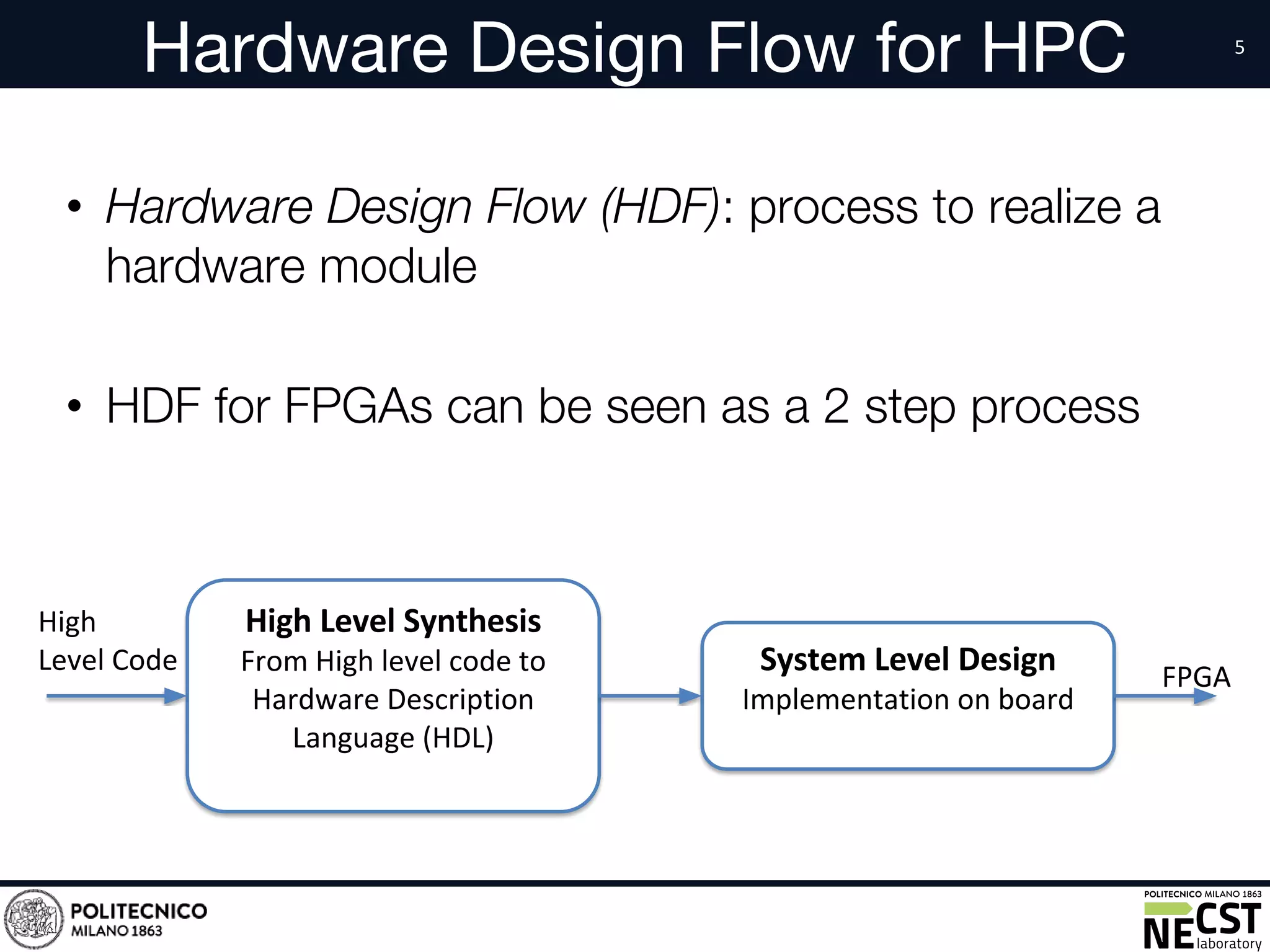

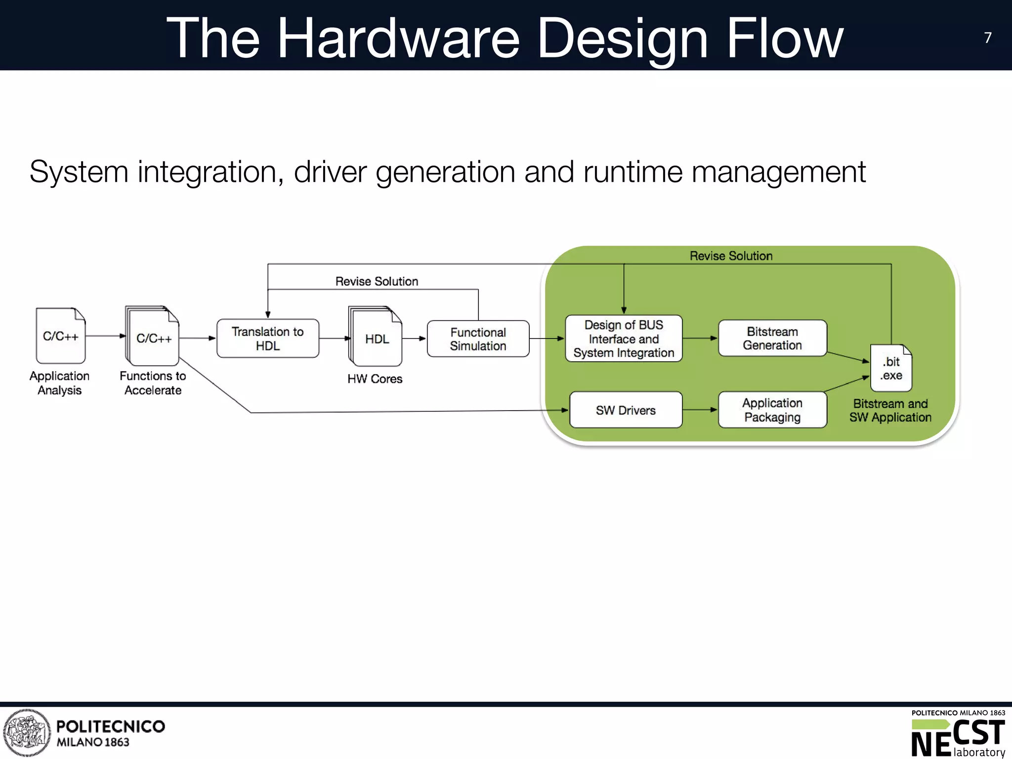


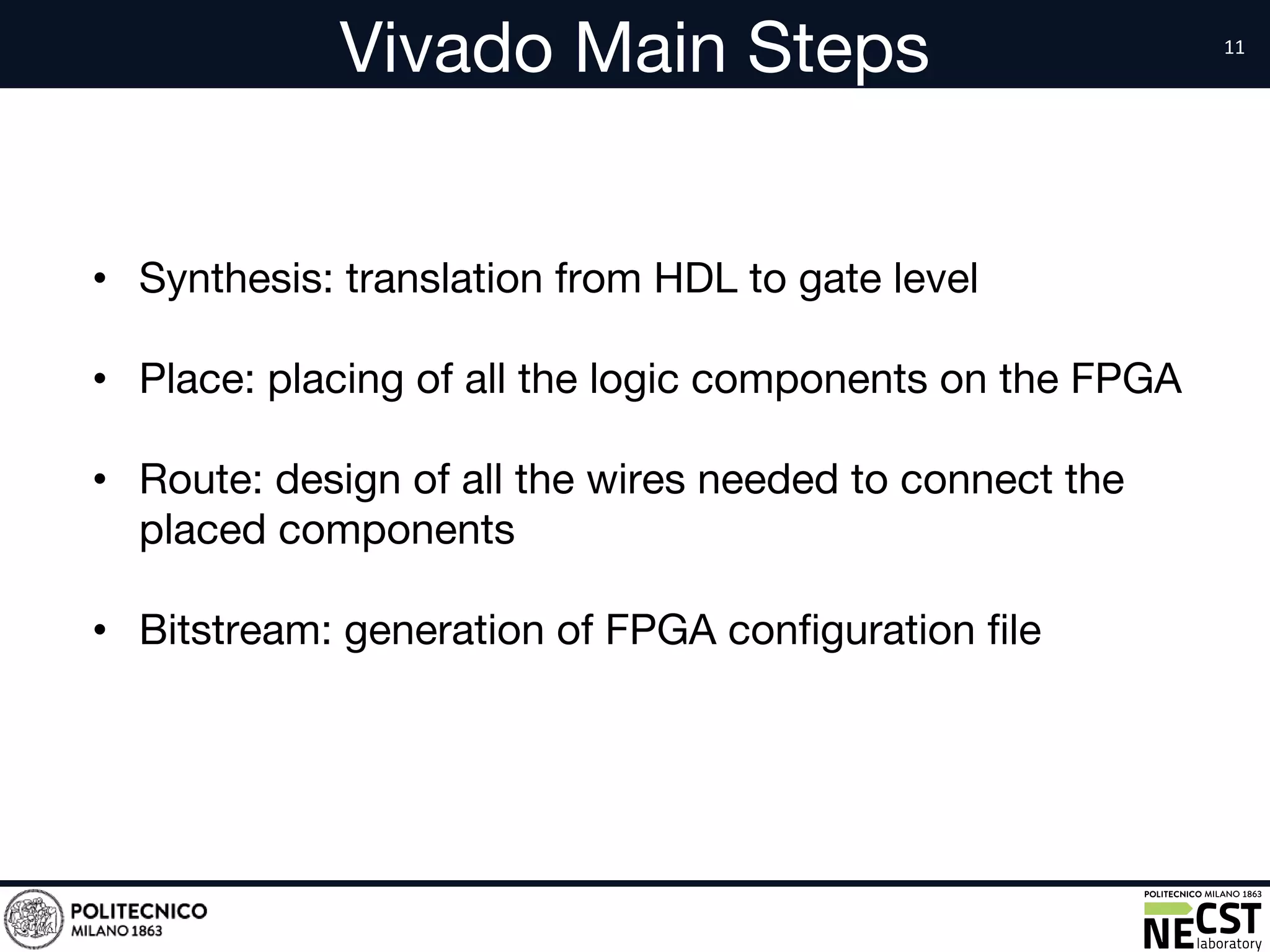
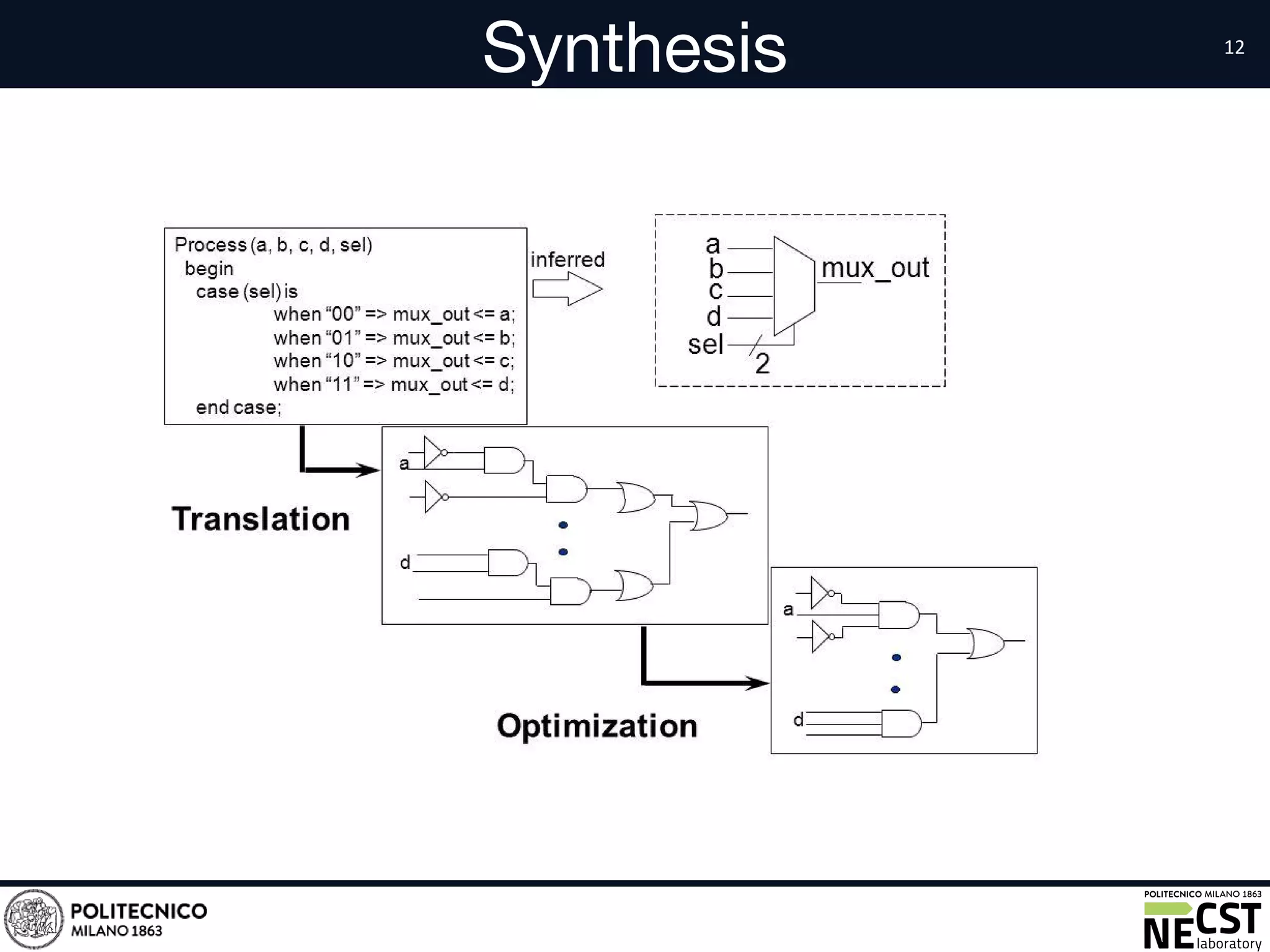
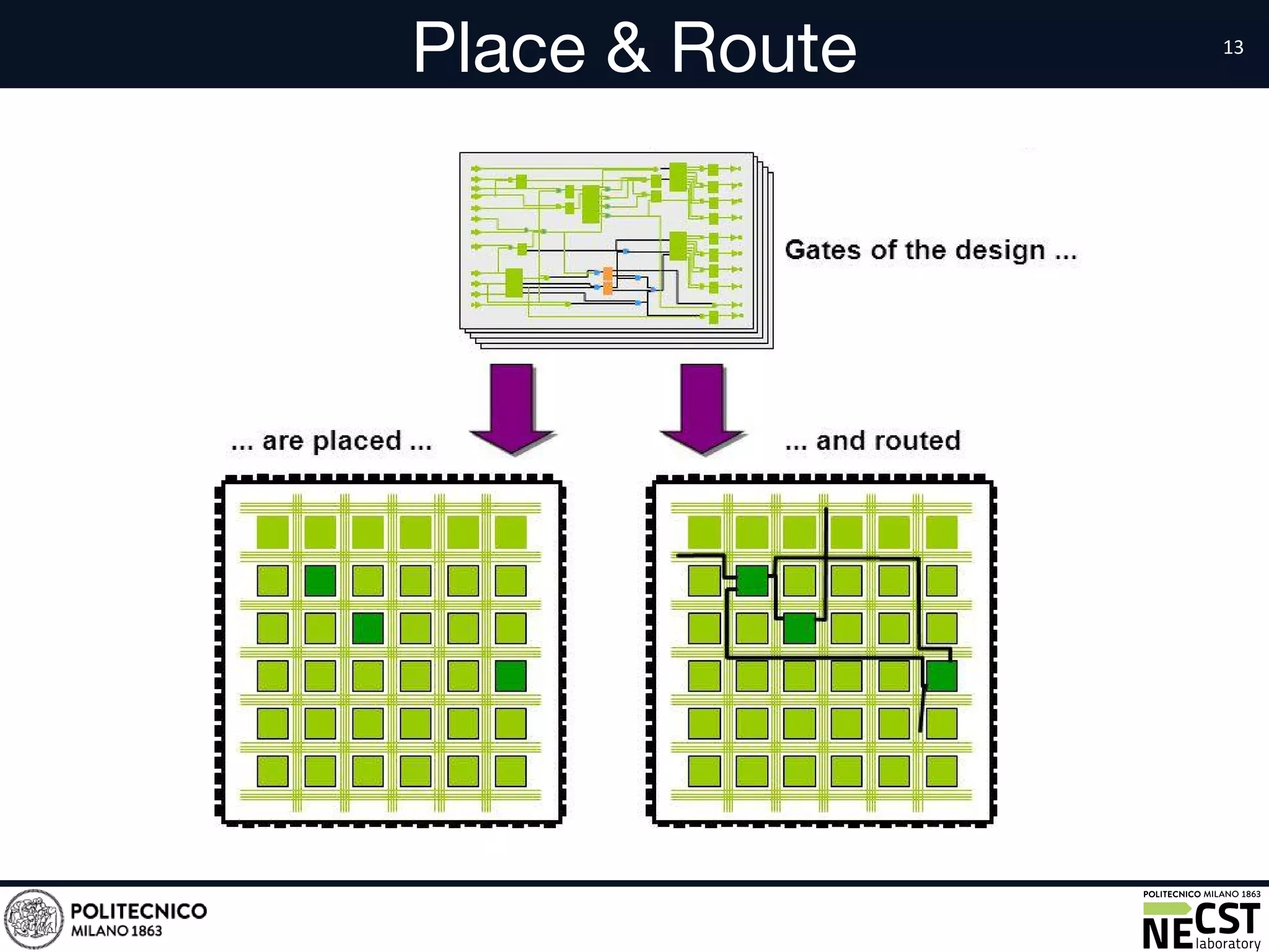


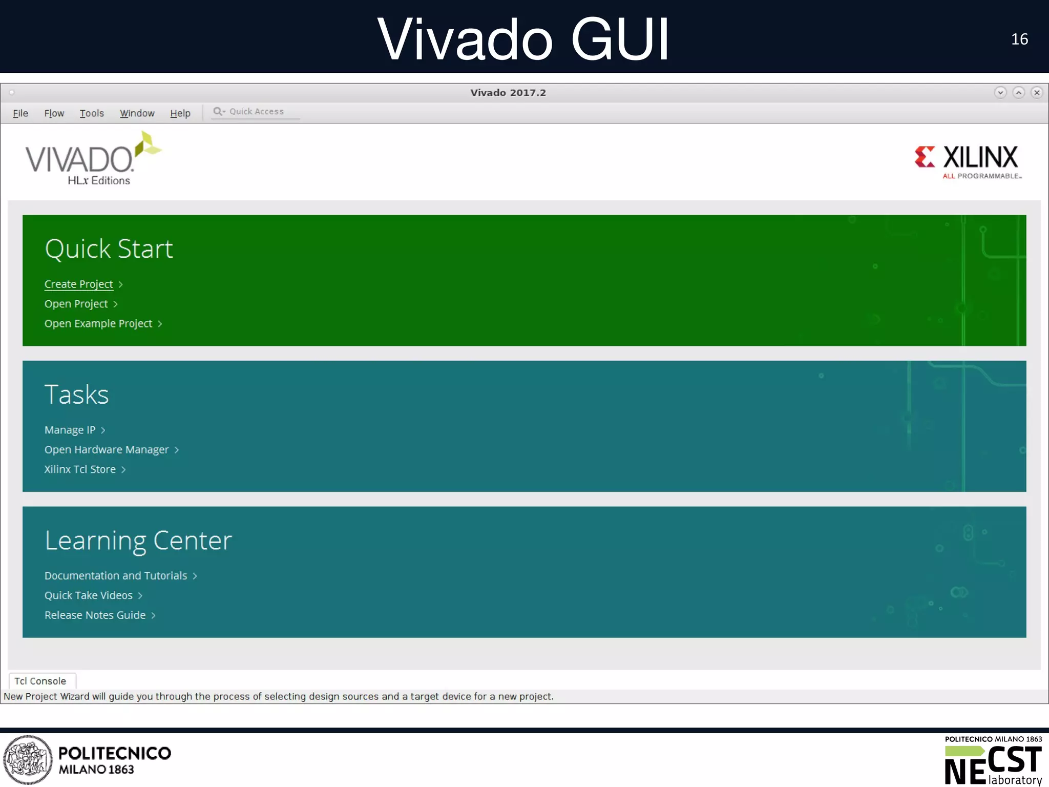


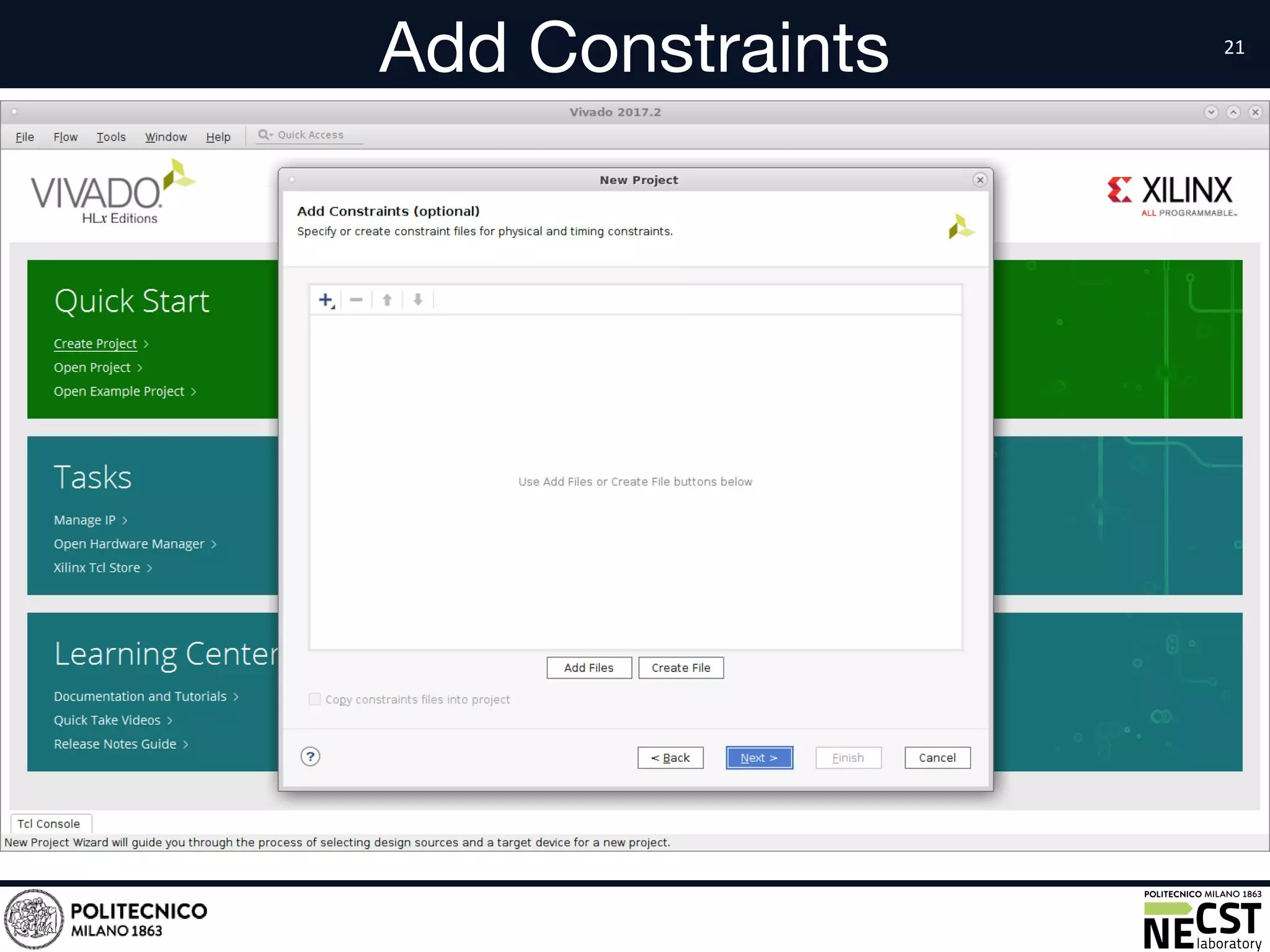
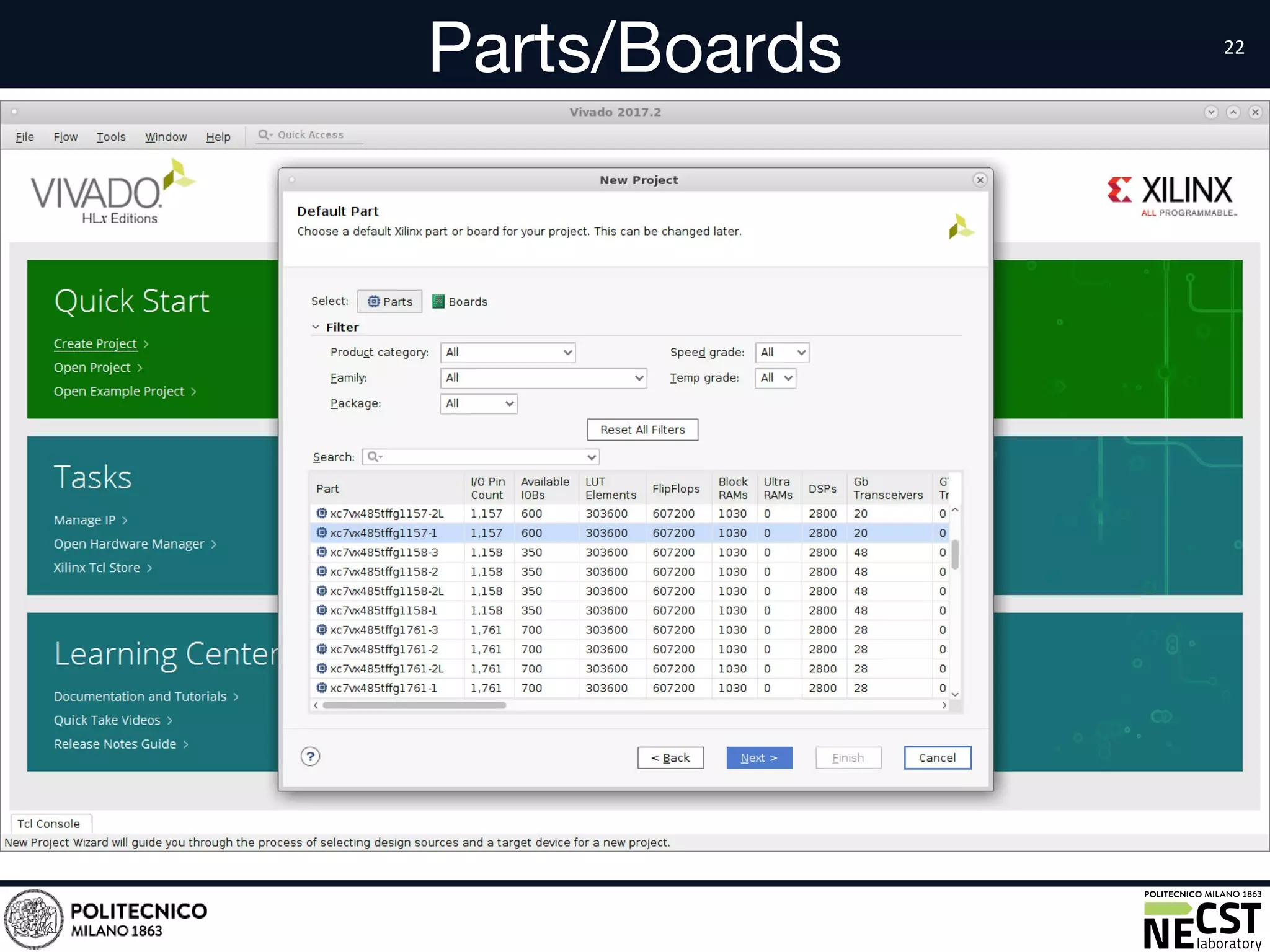
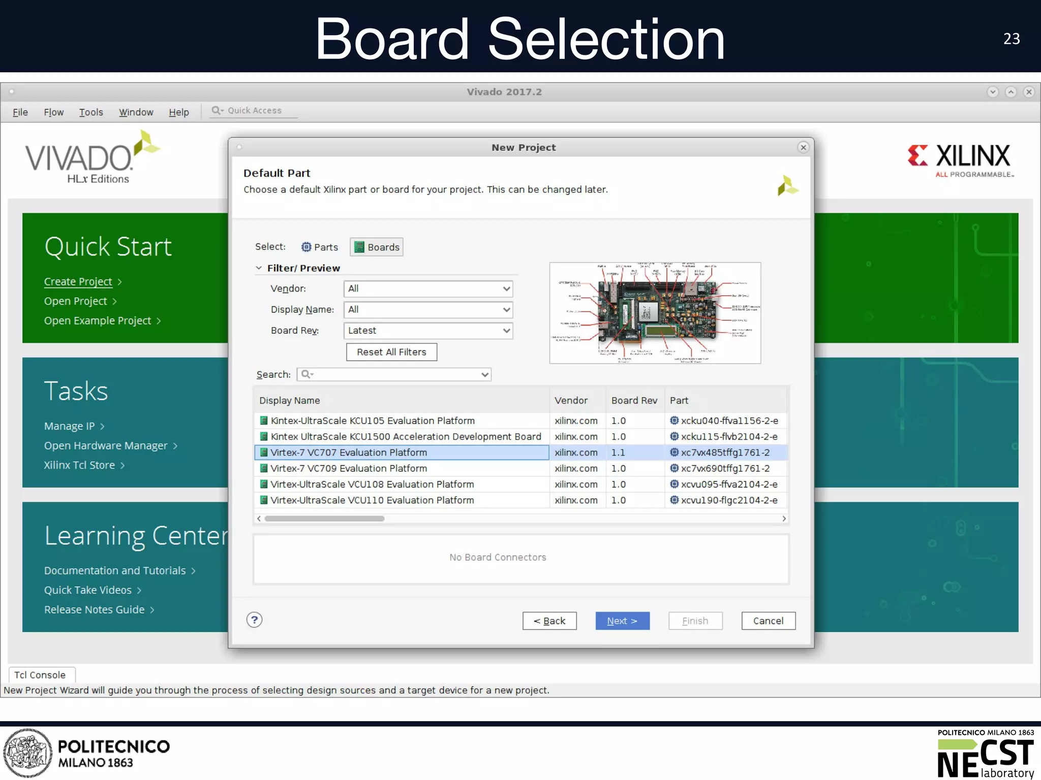

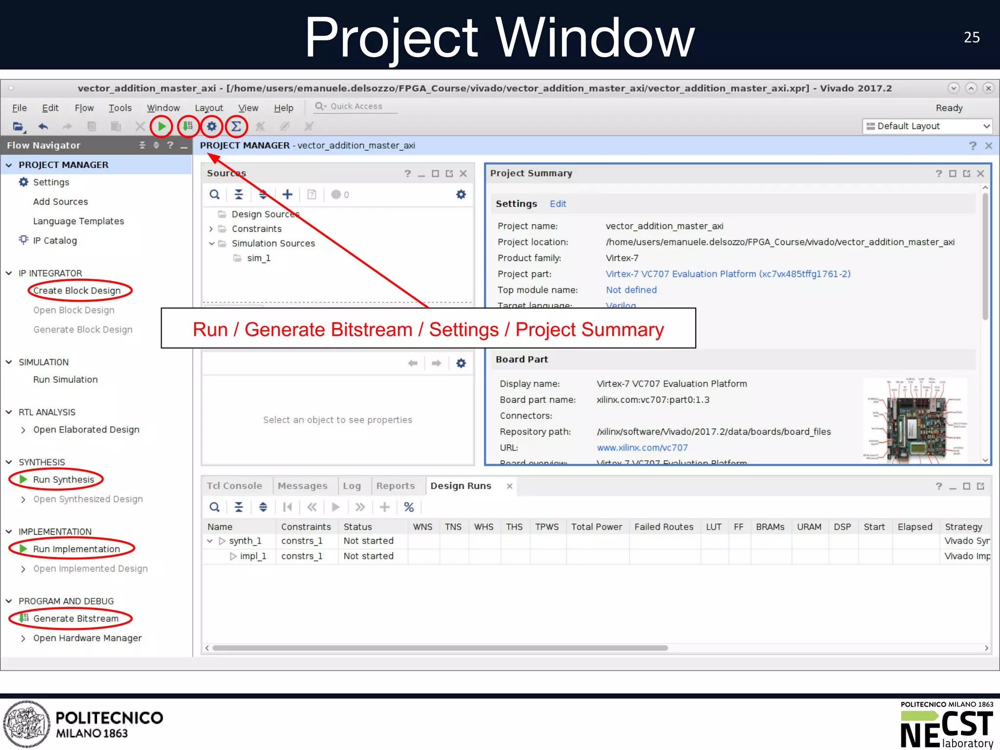


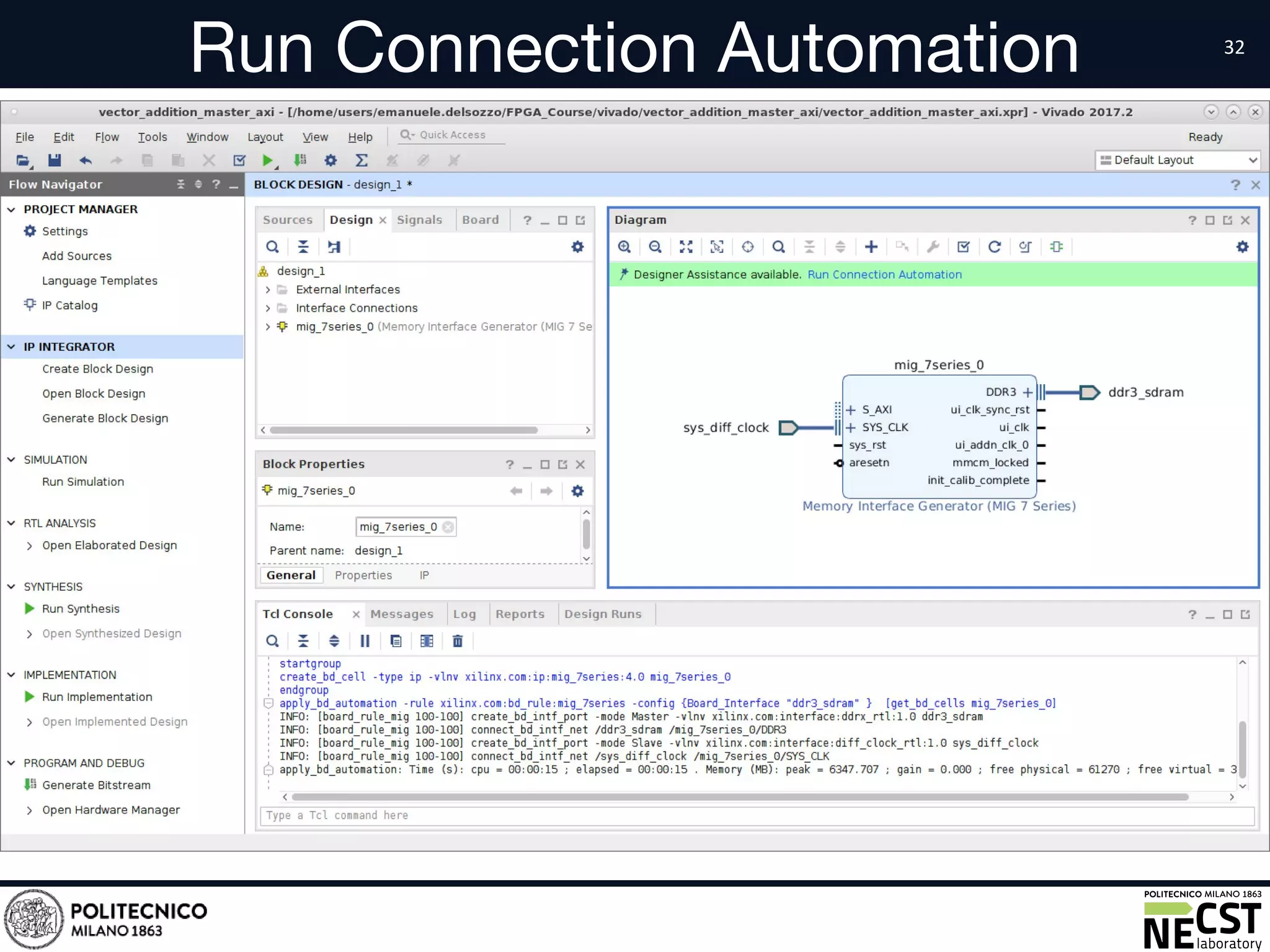


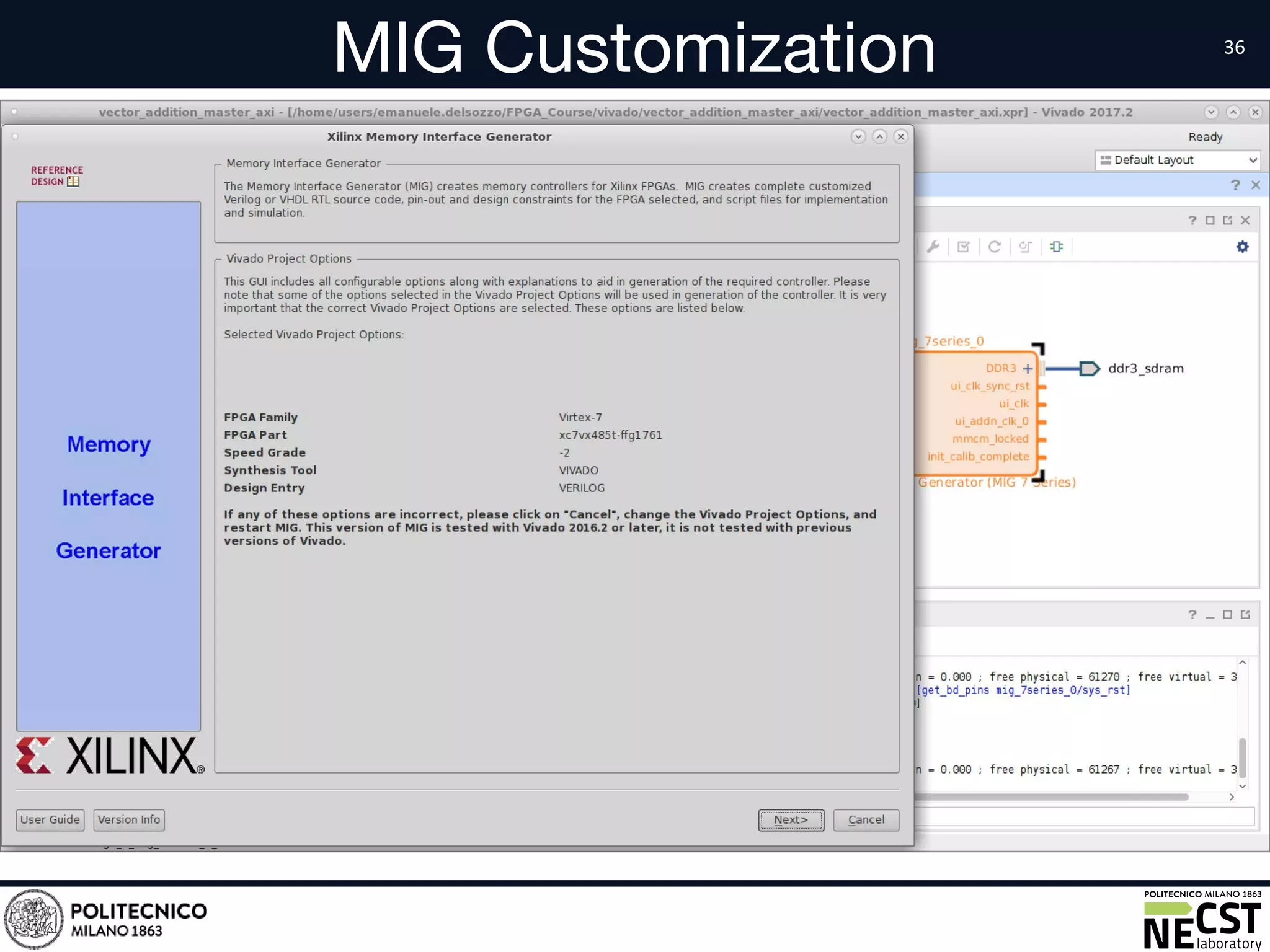
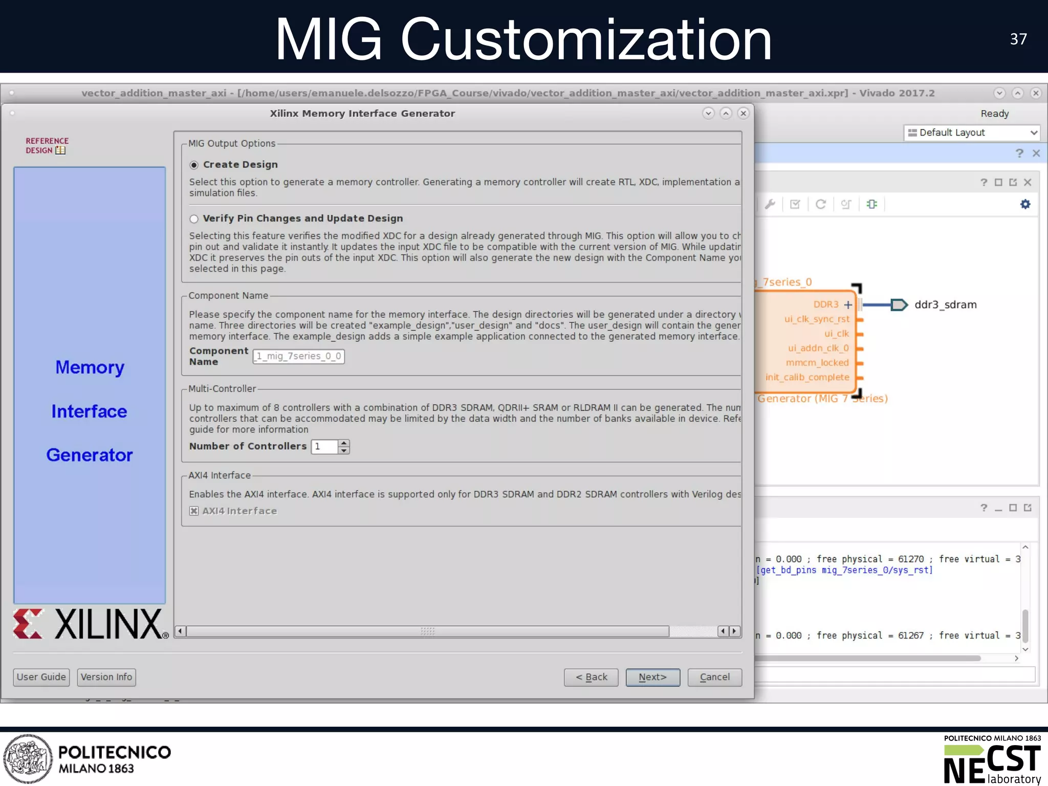


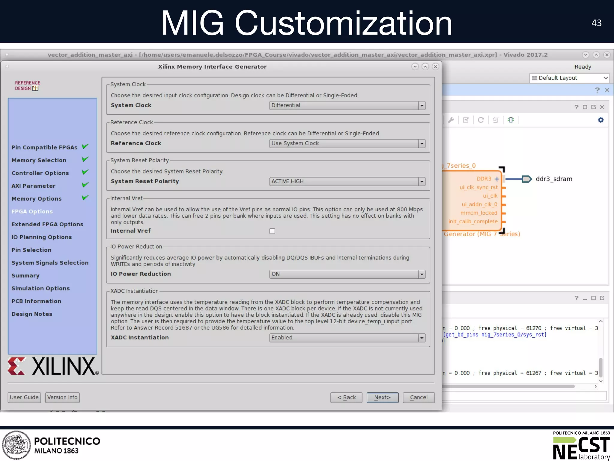
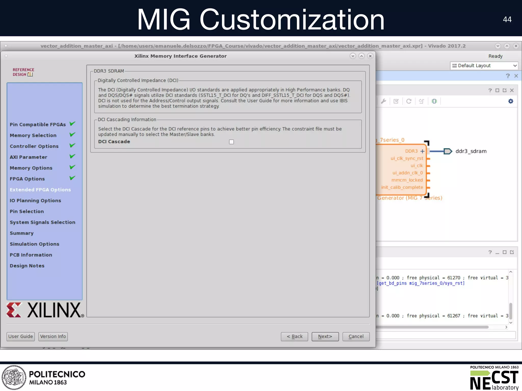
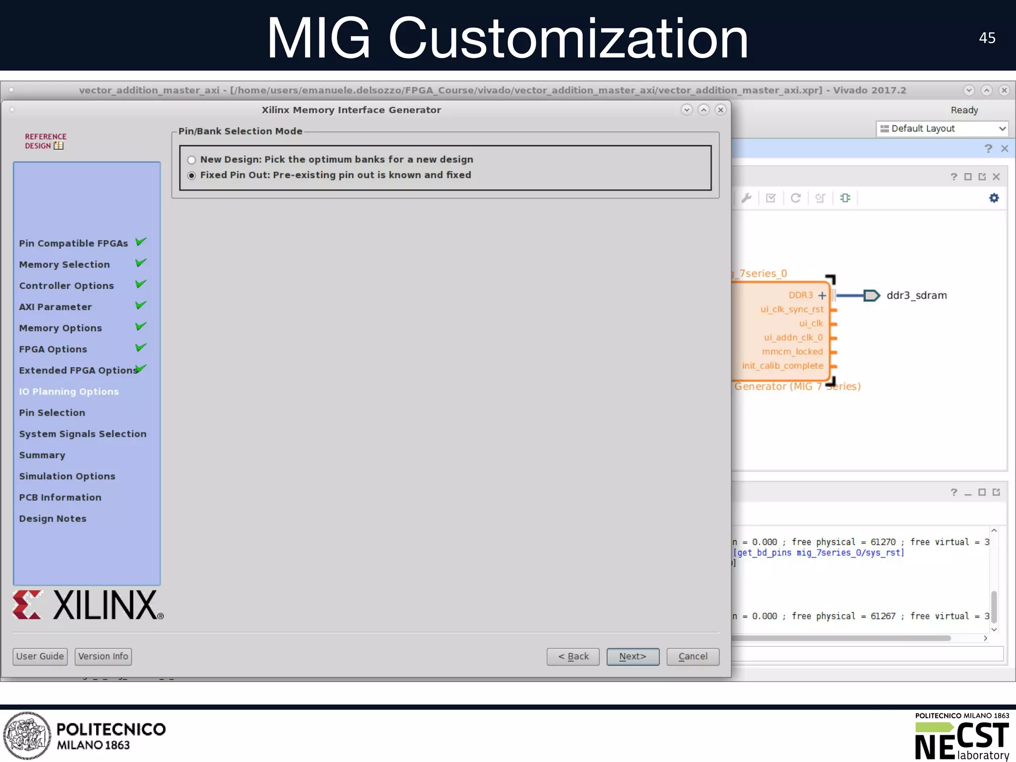
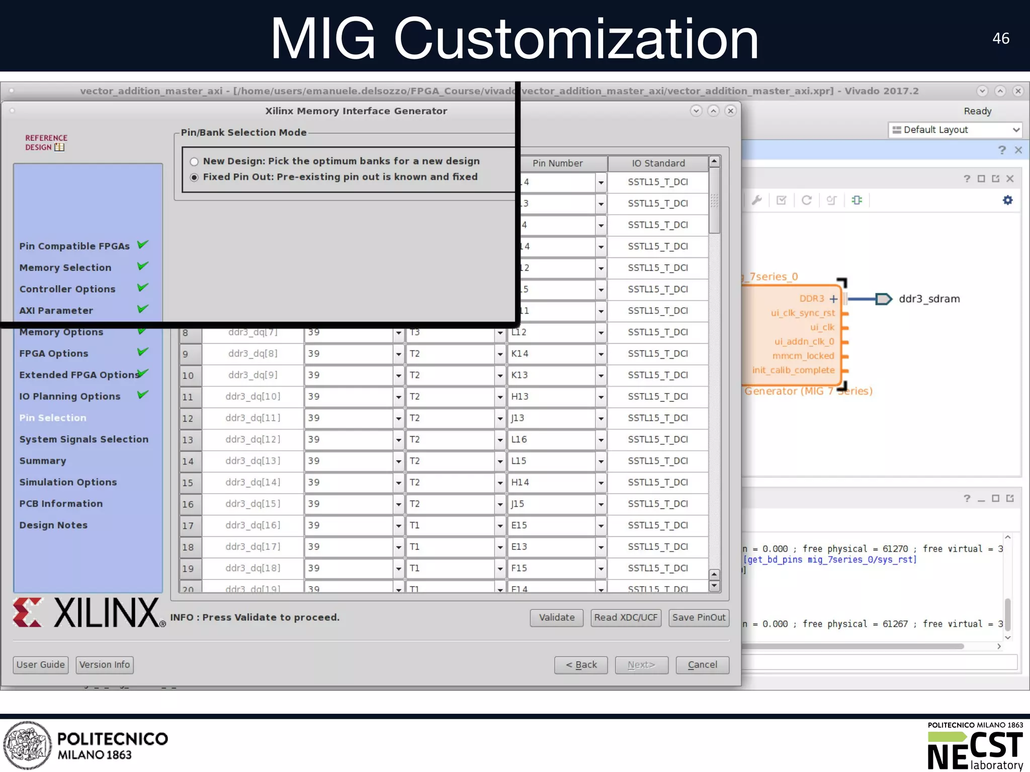


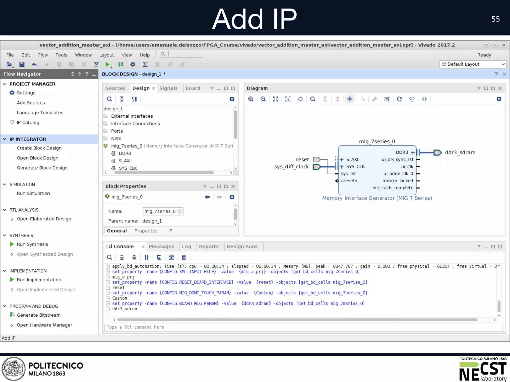

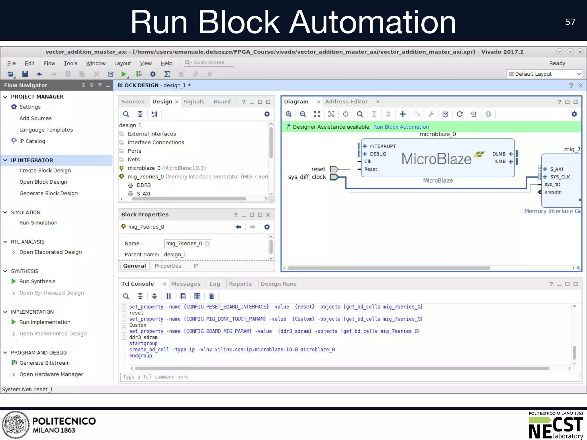


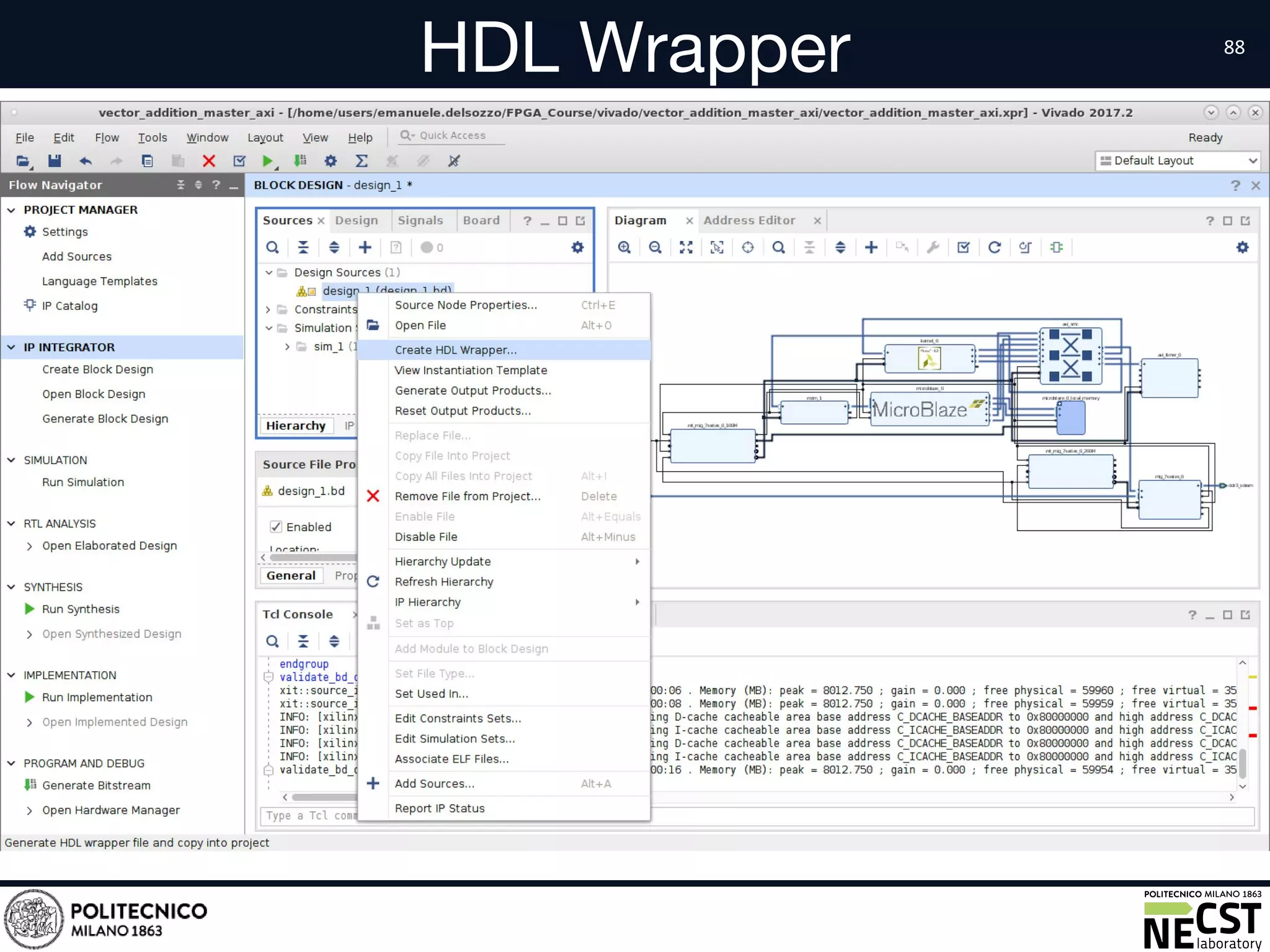
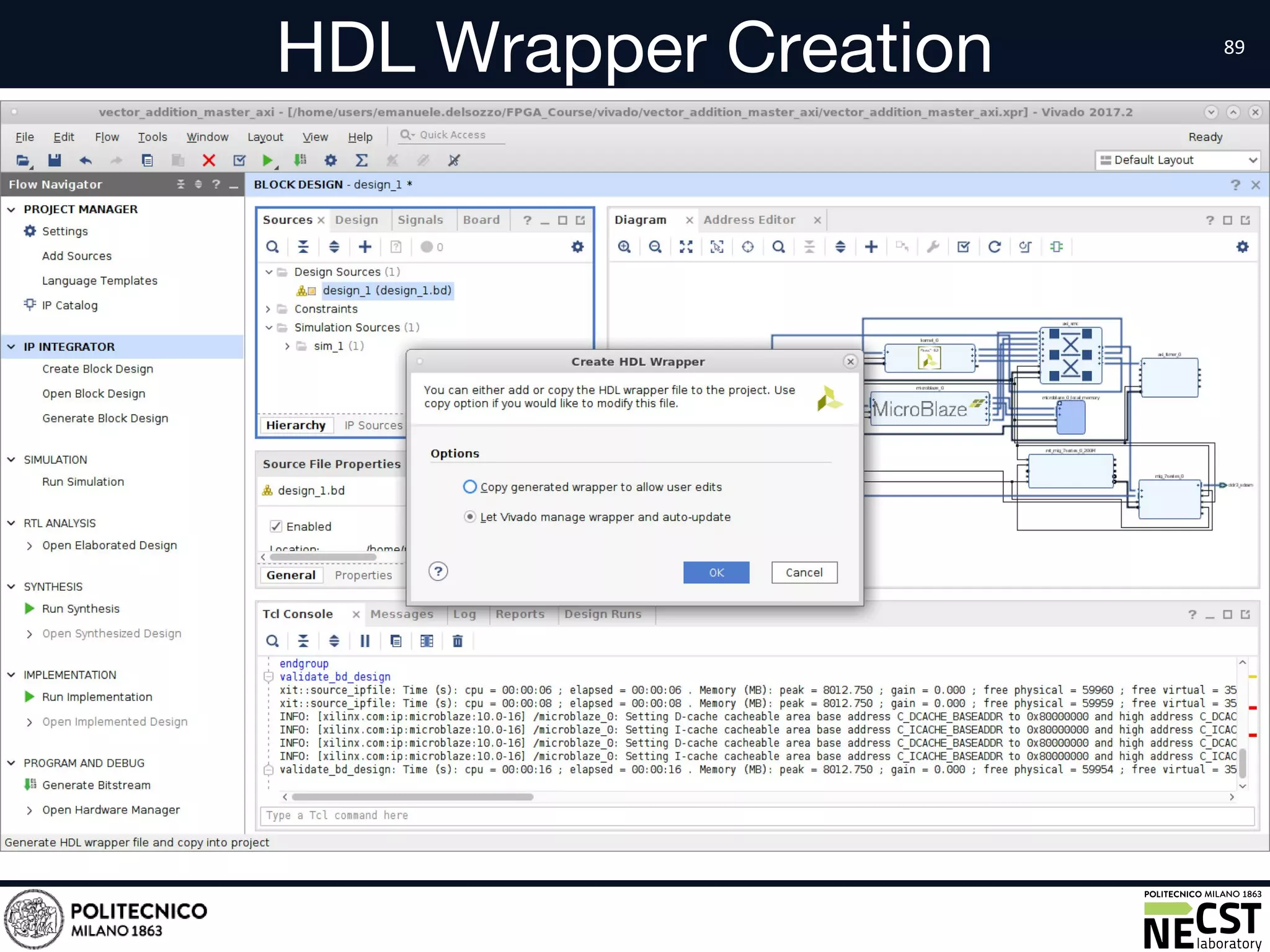


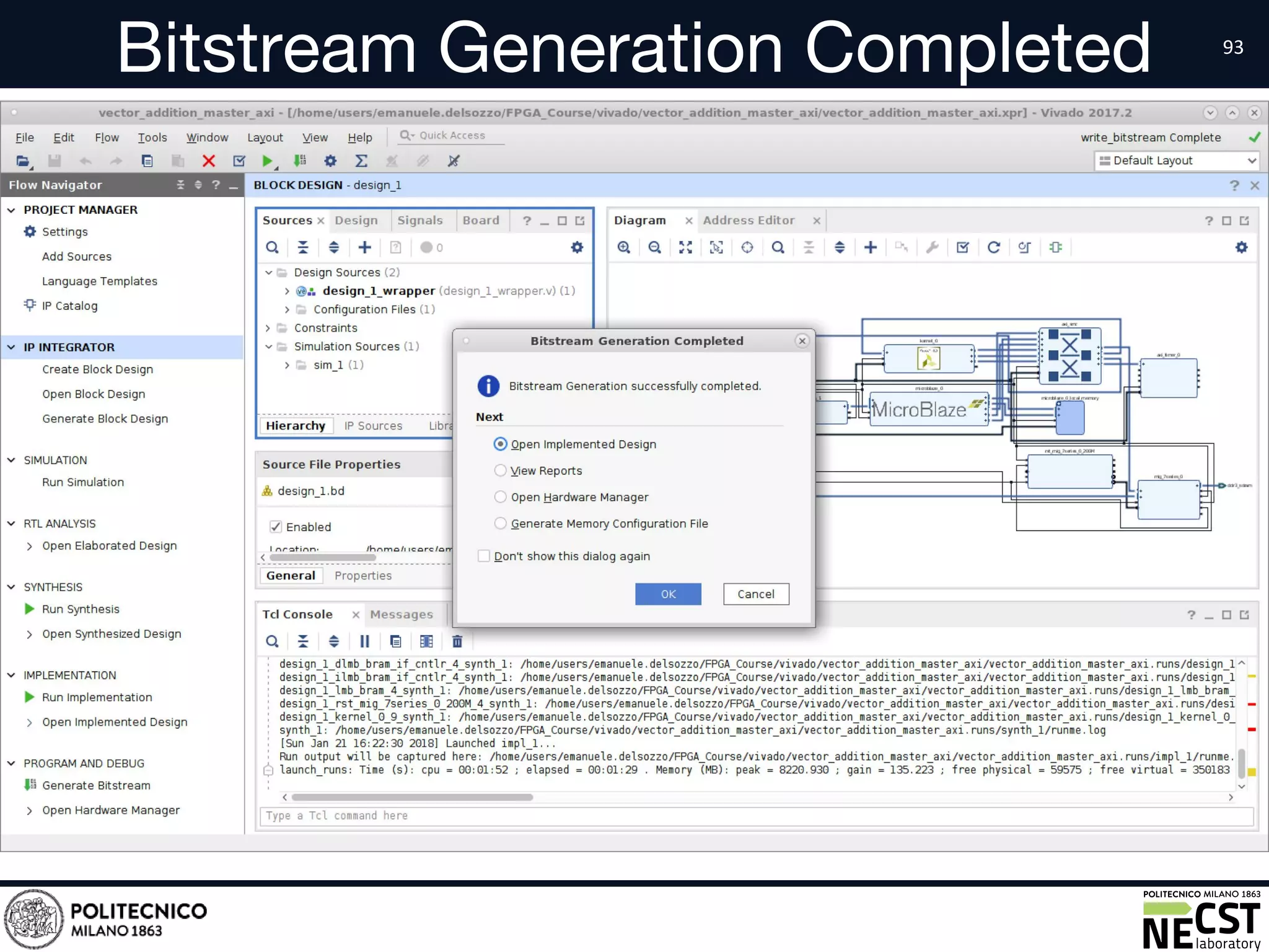


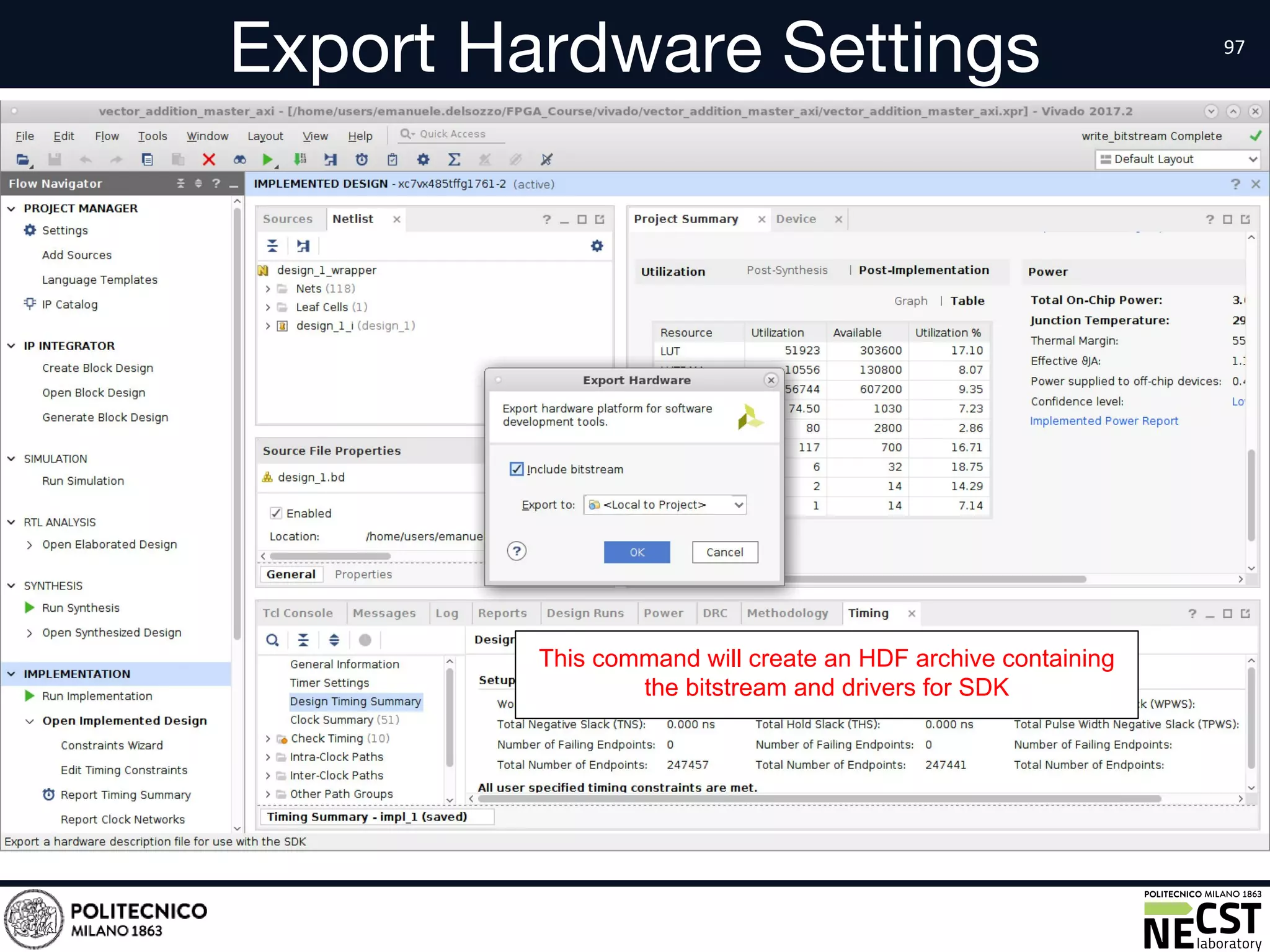
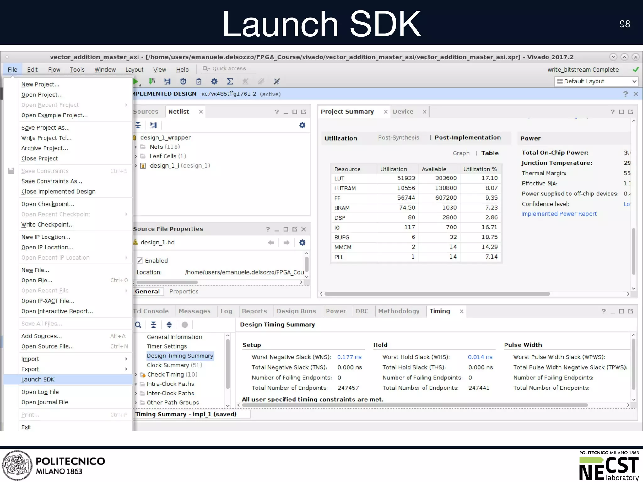

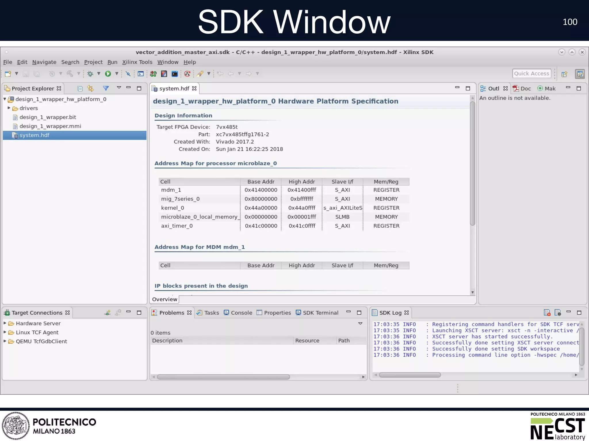

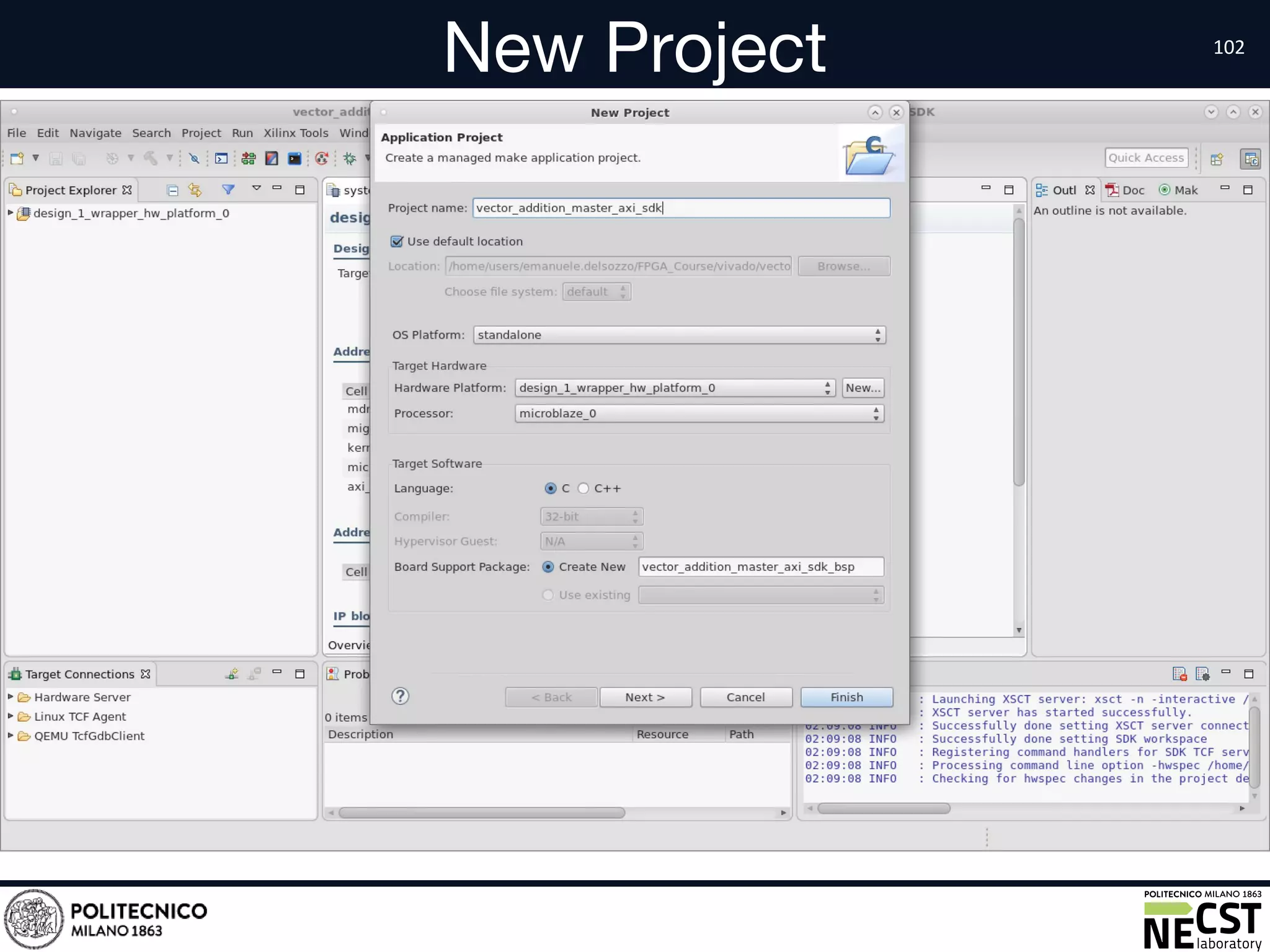
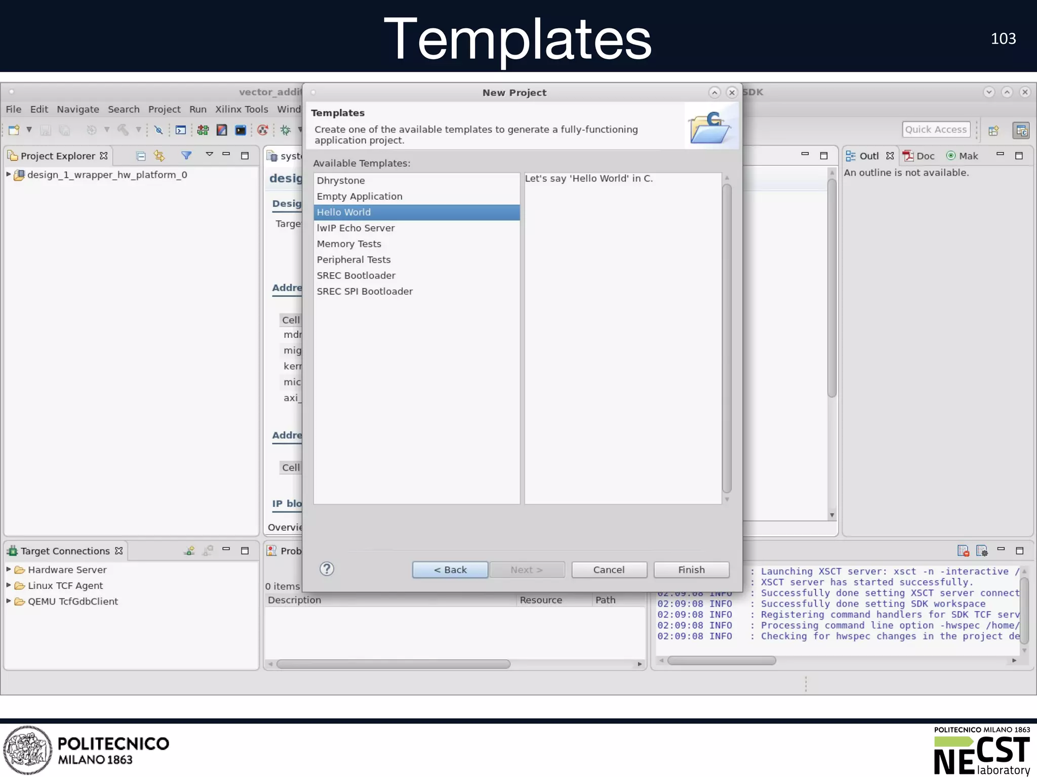
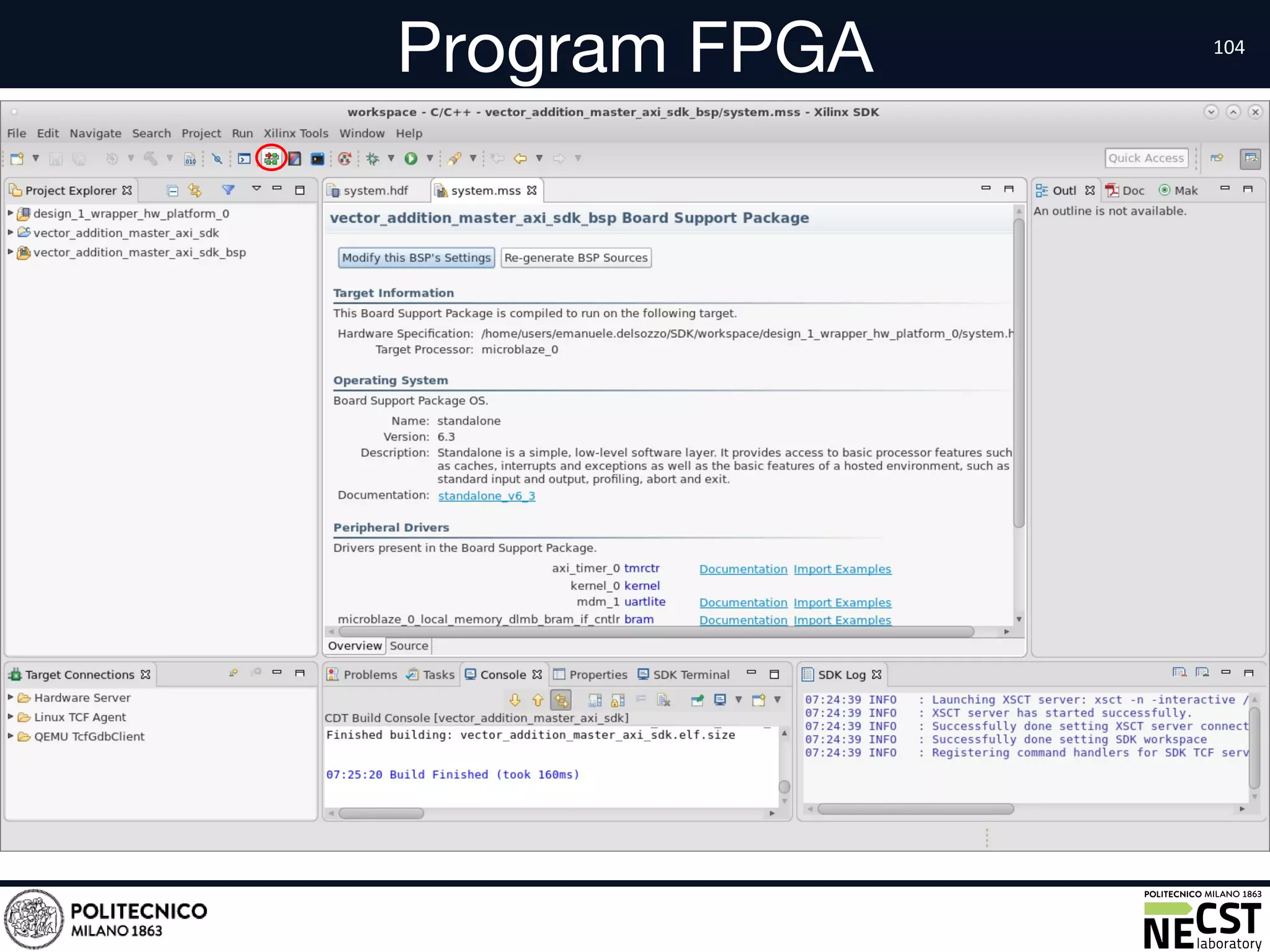

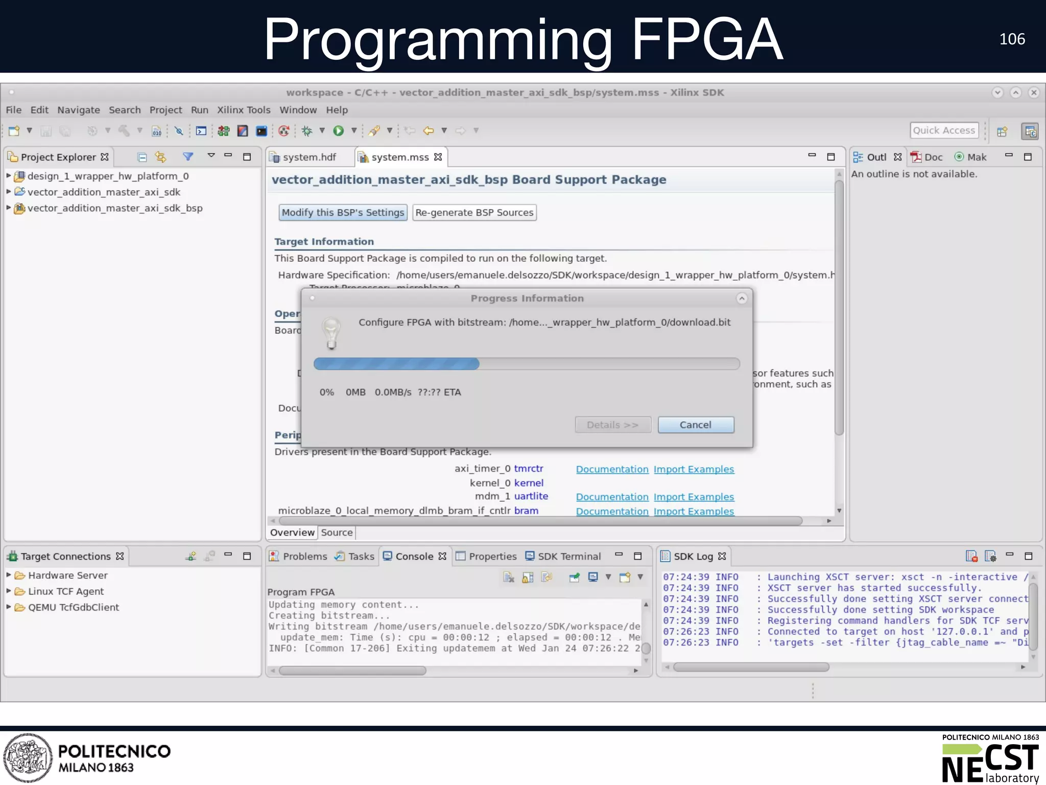
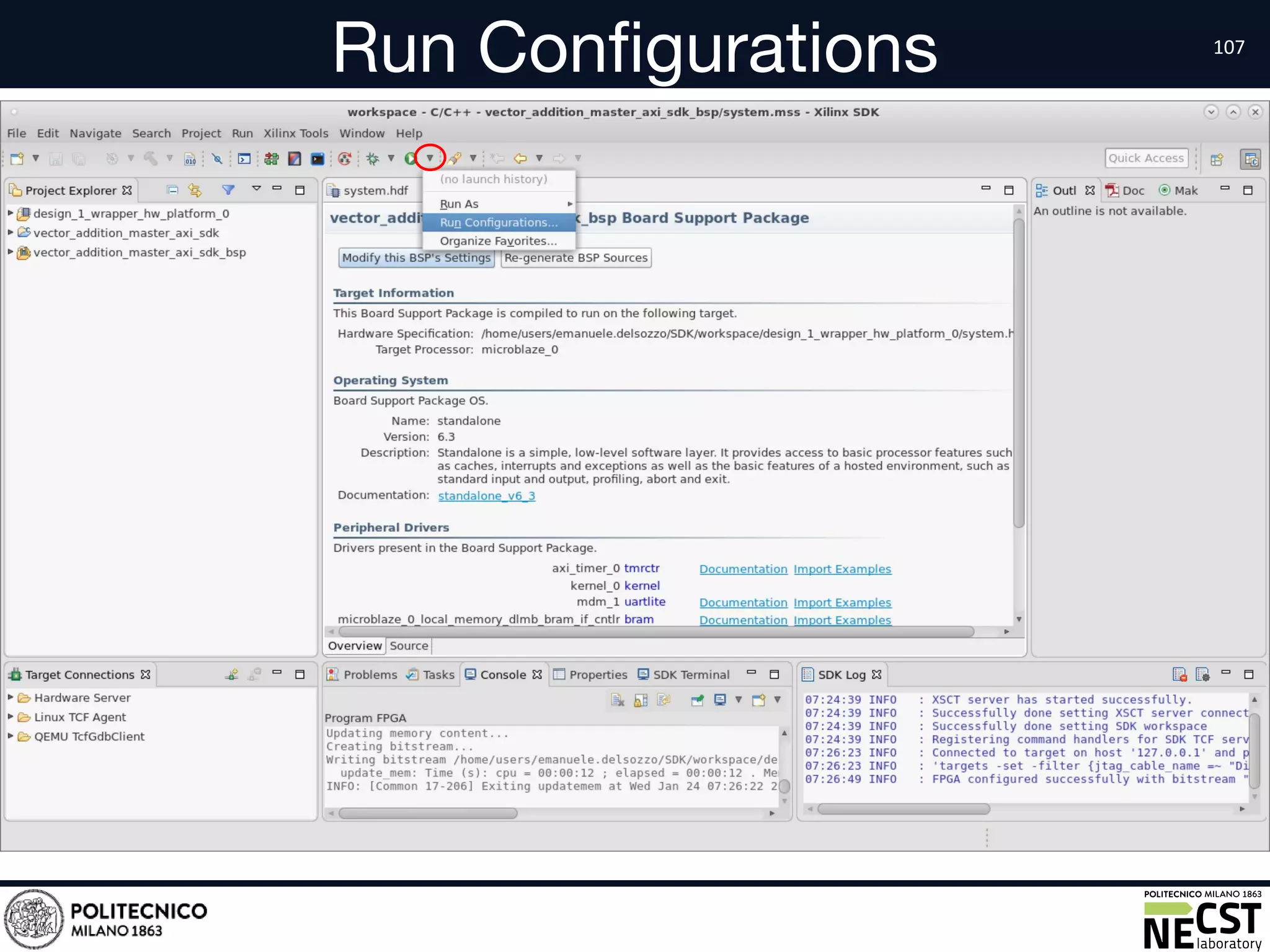
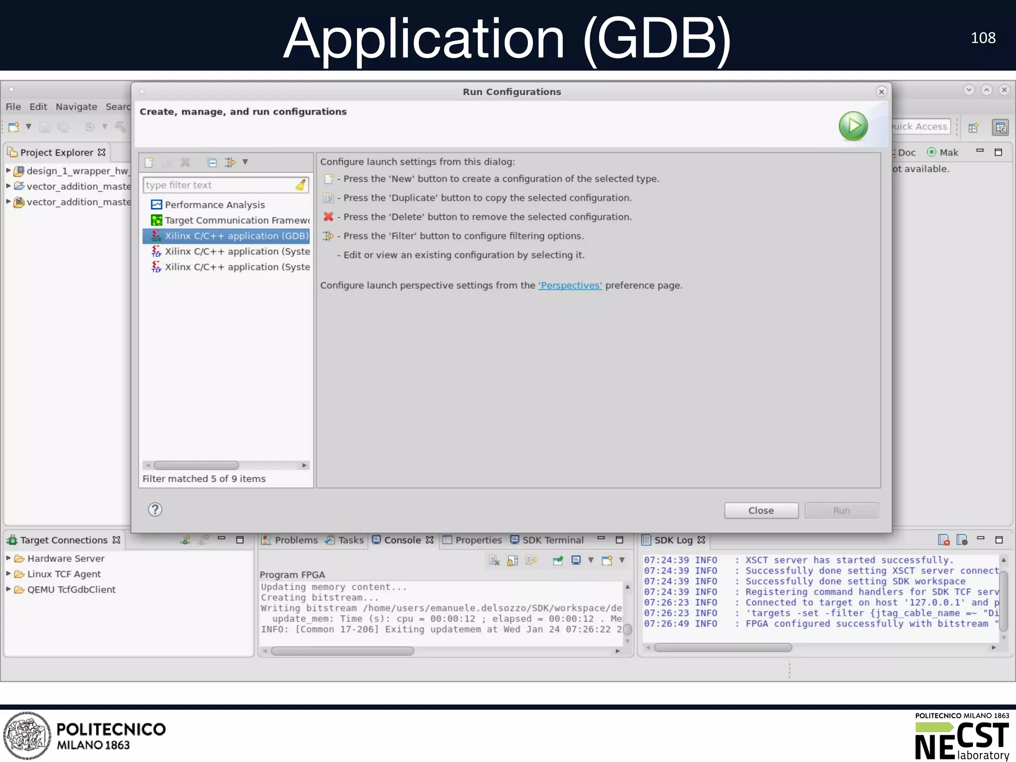
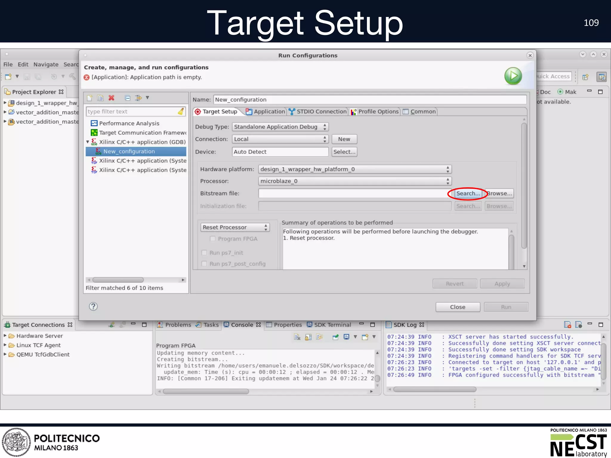
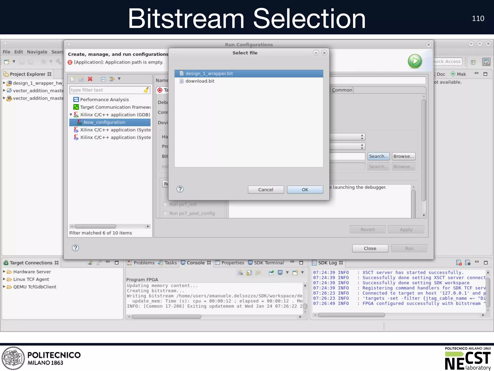
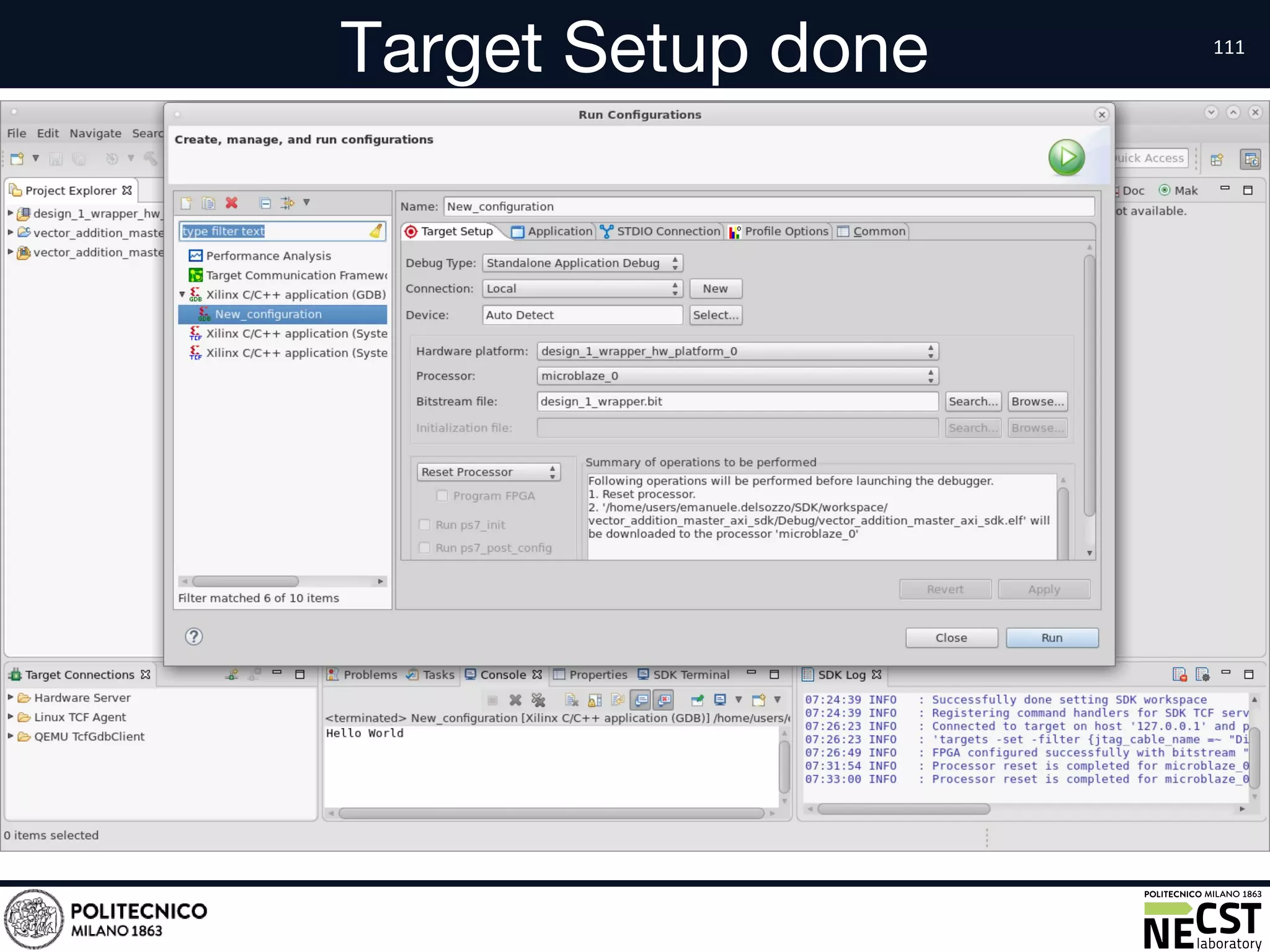
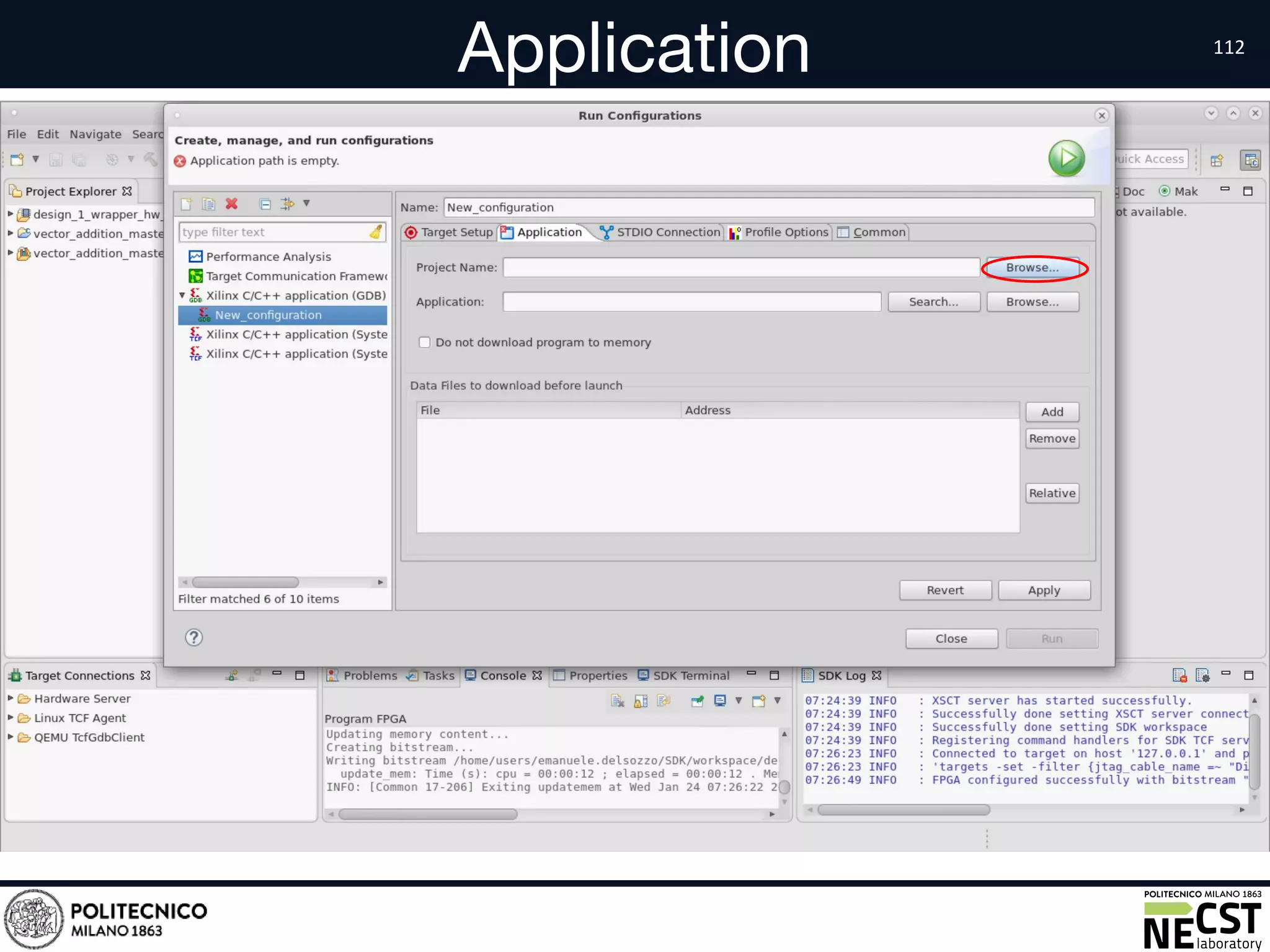


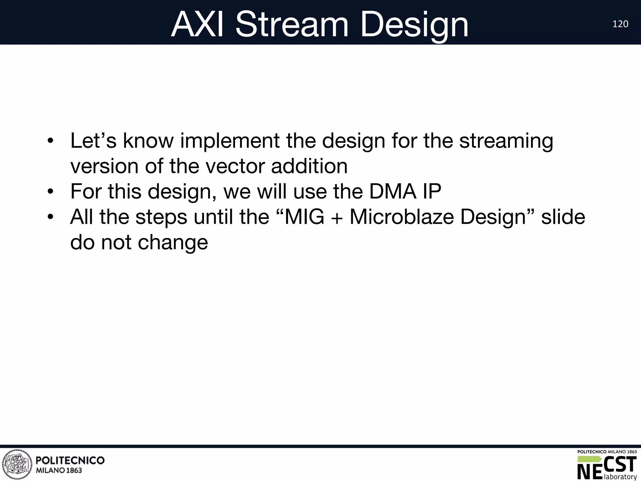
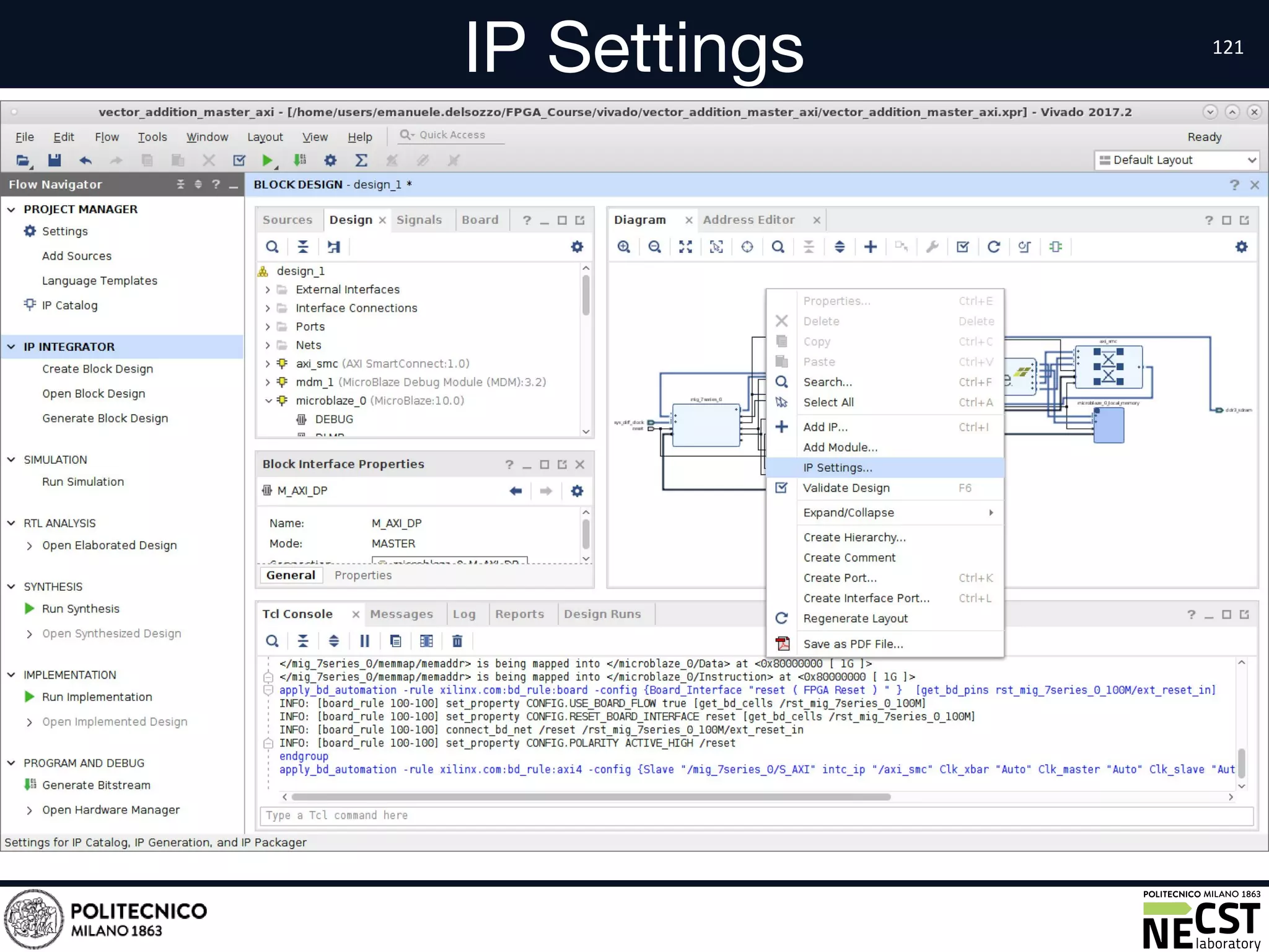


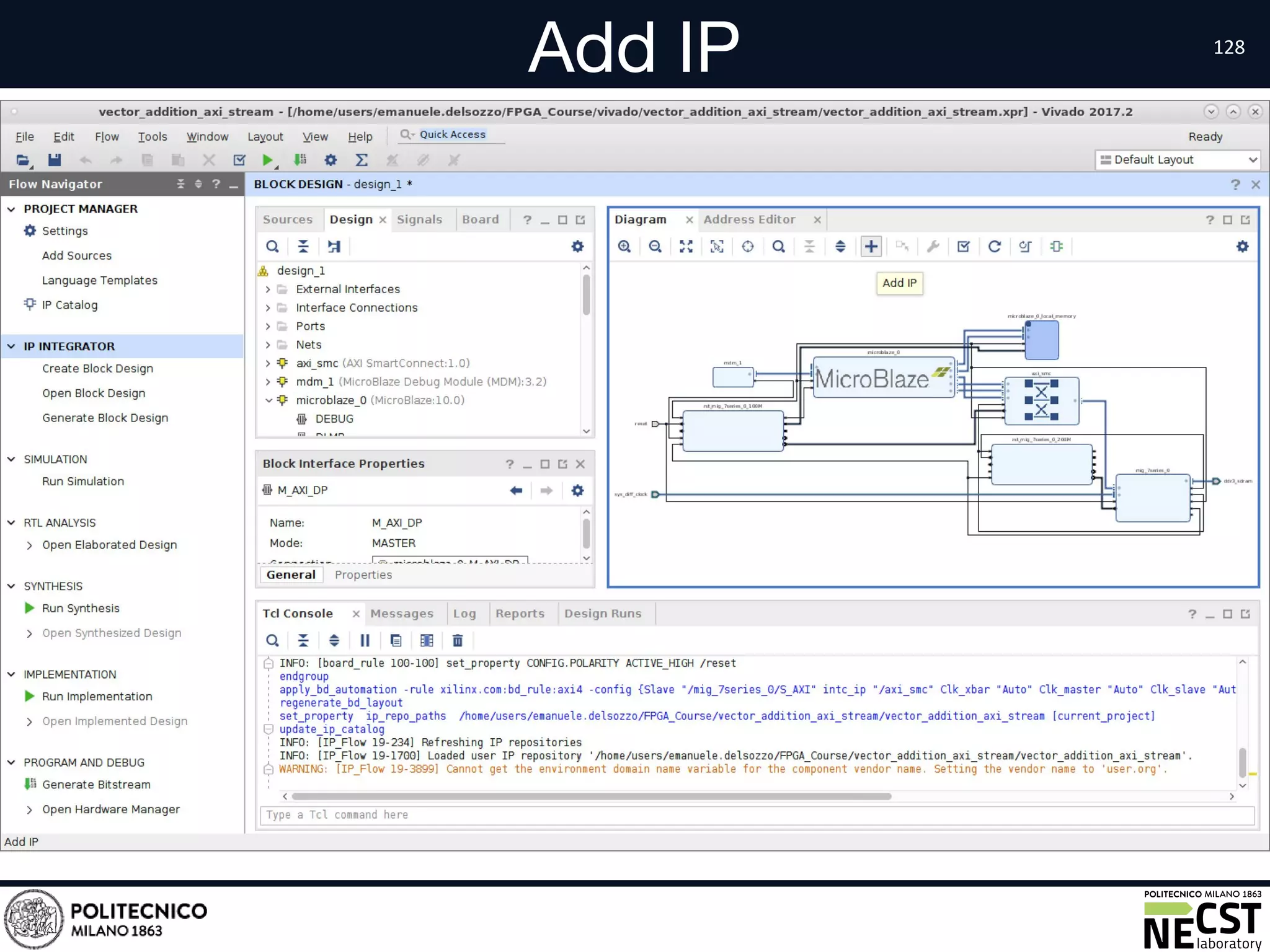


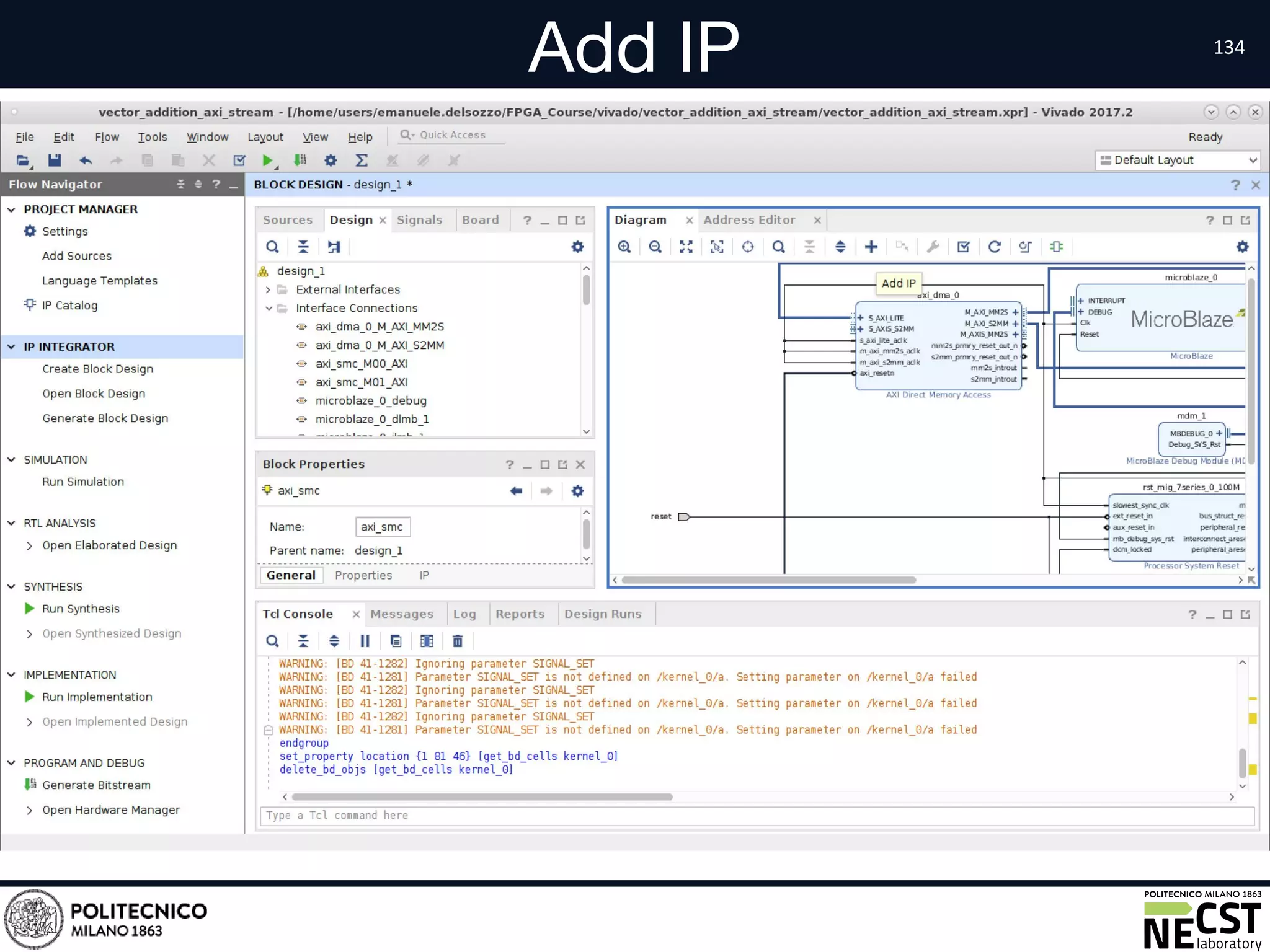

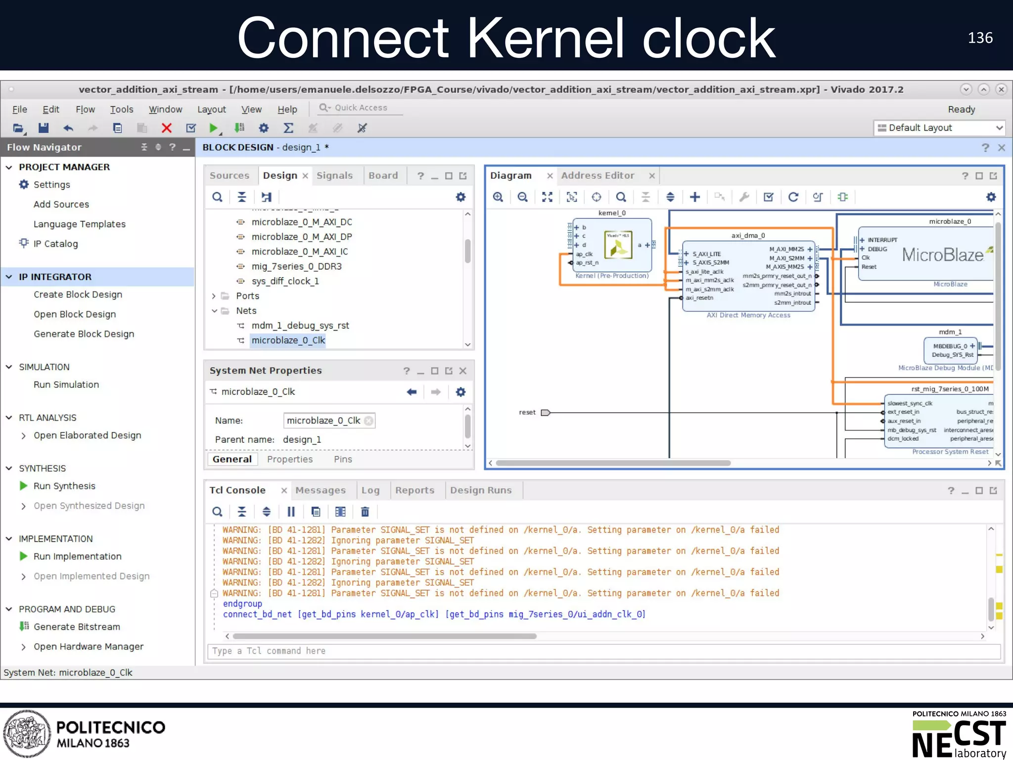

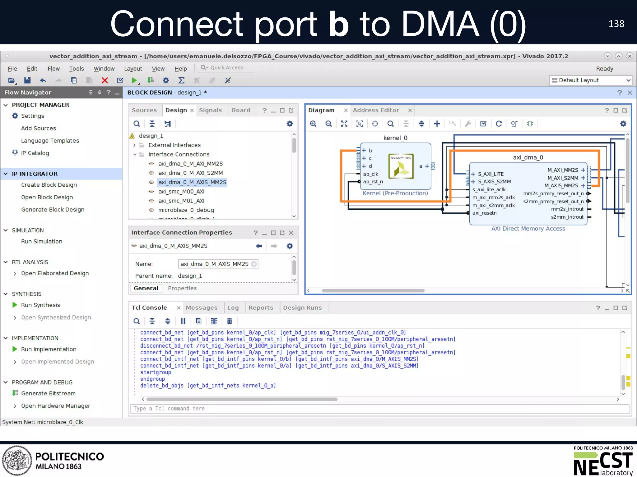

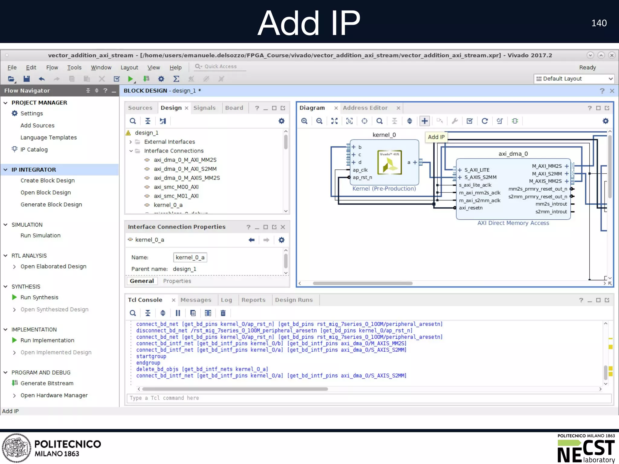


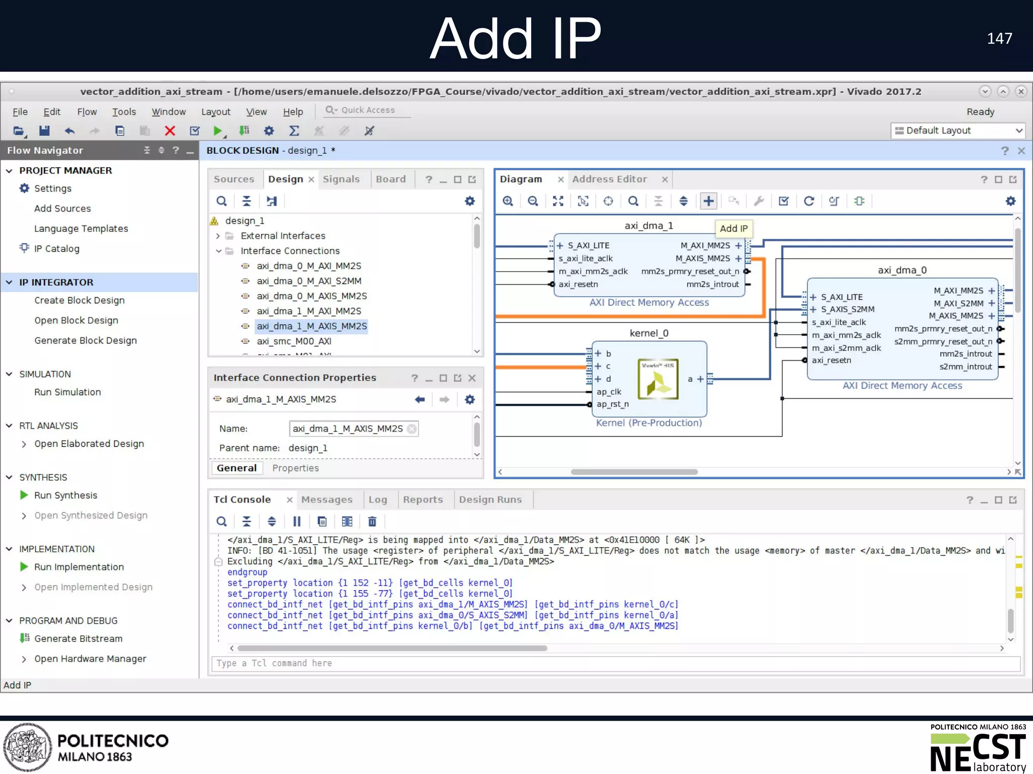


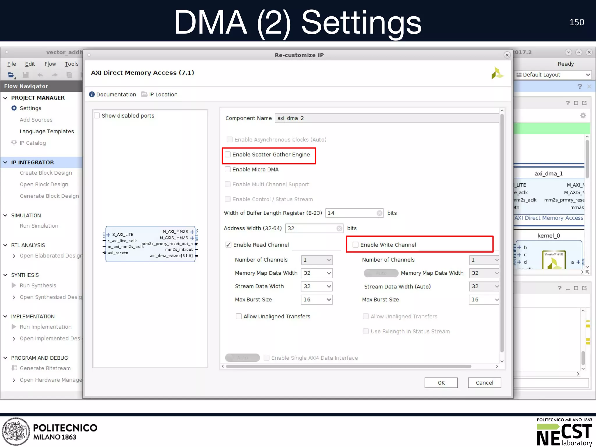

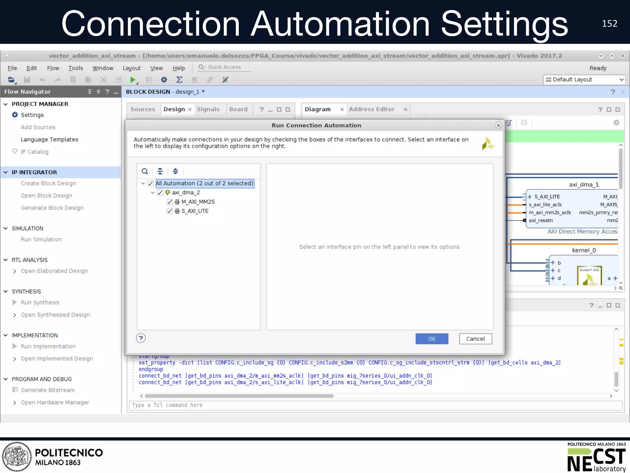


This document provides an overview of the Xilinx Vivado design suite for FPGA hardware design. It discusses the main steps in the hardware design flow including synthesis, place and route, and bitstream generation. It then demonstrates implementing designs for vector addition using both AXI master and AXI stream interfaces. The document walks through creating a Vivado project, adding IP cores like the MicroBlaze processor and memory interface, connecting the design, and generating a bitstream for the FPGA. It also discusses exporting the hardware to Xilinx SDK and running code on the MicroBlaze to test the designs.