This document provides guidance on synthesizing and simulating FPGA designs using a hardware description language (HDL) like VHDL or Verilog. It discusses the FPGA design flow, including design entry, functional simulation, synthesis, optimization, and setting timing constraints. The document also covers using Xilinx synthesis tools and reading IP cores. The overall goal is to help users successfully synthesize their HDL designs and implement them on Xilinx FPGAs.

![Chapter 1: About the Synthesis and Simulation Design Guide
Conventions
This document uses the following conventions. An example illustrates each convention.
Typographical
The following typographical conventions are used in this document:
Convention Meaning or Use Example
Courier font Messages, prompts, and program files speed grade: - 100
that the system displays
Courier bold Literal commands that you enter in a ngdbuild design_name
syntactical statement
Helvetica bold Commands that you select from a File > Open
menu
Keyboard shortcuts Ctrl+C
Italic font Variables in a syntax statement for ngdbuild design_name
which you must supply values
References to other manuals See the Command Line Tools User Guide
for more information.
Emphasis in text If a wire is drawn so that it overlaps
the pin of a symbol, the two nets are
not connected.
Square brackets [ ] An optional entry or parameter. ngdbuild [option_name]
However, in bus specifications, such as design_name
bus[7:0], they are required.
Braces { } A list of items from which you must lowpwr ={on|off}
choose one or more
Vertical bar | Separates items in a list of choices lowpwr ={on|off}
Vertical ellipsis Repetitive material that has been IOB #1: Name = QOUT IOB #2:
omitted Name = CLKIN
.
.
.
Horizontal ellipsis . . . Repetitive material that has been allow block . . . block_name
omitted loc1 loc2 ... locn;
Online Document
The following conventions are used in this document:
Convention Meaning or Use Example
Blue text Cross-reference link See the section Additional Resources
for details.
Refer to Title Formats in Chapter 1 for
details.
See Figure 2-5 in the Virtex®-6
Handbook.
Synthesis and Simulation Design Guide
UG626 (v 11.4) December 2, 2009 www.xilinx.com 13](https://image.slidesharecdn.com/sim-120220090038-phpapp01/85/Sim-13-320.jpg)

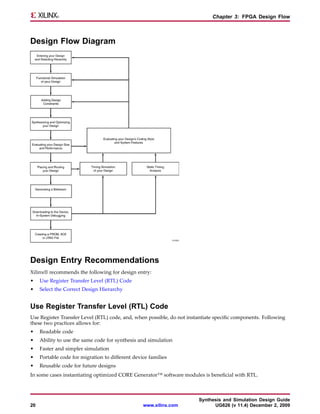


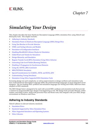
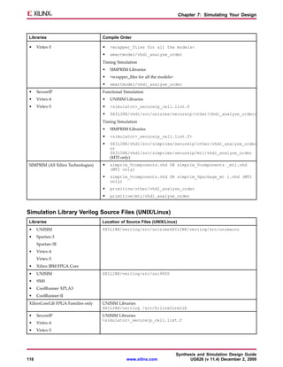
![Chapter 3: FPGA Design Flow
A typical design for a Virtex®-4 device or a Virtex-5 device should allow 40% of the delay for logic, and 60%
of the delay for routing. If most of your time is taken by logic, the design will probably not meet timing after
Place and Route.
Mapping Your Design Using the Command Line
For available options, enter the trce command at the command line without any arguments.
To map your design using the command line:
1. To translate your design, run:
ngdbuild -p target_device design_name.edf (or ngc)
2. To map your design, run:
map design_name.ngd
3. Use a text editor to view the Device Summary section of the Map Report <design_name.mrp>.
The Device Summary section contains the device utilization information.
4. Run a timing analysis of the logic level delays from your mapped design as follows:
trce [options] design_name.ncd
Use the TRACE reports to:
• See how well the design meets performance goals
• Decide whether to proceed to Place and Route, or to modify your design or implementation options
Leave some slack in routing delays to allow the Place and Route tools to successfully complete your design.
Evaluating Coding Style and System Features
If you are not satisfied with design performance, re-evaluate your code. Modifying your code and selecting
different compiler options can dramatically improve device utilization and speed.
Modifying Your Code to Improve Design Performance
To improve design performance:
1. Reduce levels of logic to improve timing by:
a. Using pipelining and re-timing techniques
b. Rewriting the Hardware Description Language (HDL) descriptions
c. Enabling or disabling resource sharing
2. Restructure logic to redefine hierarchical boundaries to help the compiler optimize design logic
3. Perform logic replication to reduce critical nets fanout to improve placement and reduce congestion
4. Take advantage of device resource with the CORE Generator™ software modules
Improving Resource Utilization Using FPGA System Features
After correcting any coding problems, use the following FPGA system features to improve resource utilization
and enhance the speed of critical paths:
• Use clock enables.
• Use one-hot encoding for large or complex state machines.
• Use I/O registers when applicable.
• Use dedicated shift registers.
• In Virtex®-4 devices and Virtex-5 devices, use the dedicated DSP blocks.
Synthesis and Simulation Design Guide
UG626 (v 11.4) December 2, 2009 www.xilinx.com 29](https://image.slidesharecdn.com/sim-120220090038-phpapp01/85/Sim-29-320.jpg)
![Chapter 4: General Recommendations for Coding Practices
VHDL Generic Coding Example
-- FIFO_WIDTH data width (number of bits)
-- FIFO_DEPTH by number of address bits
-- for the FIFO RAM i.e. 9 -> 2**9 -> 512 words
-- FIFO_RAM_TYPE: BLOCKRAM or DISTRIBUTED_RAM
-- Note: DISTRIBUTED_RAM suggested for FIFO_DEPTH
-- of 5 or less
entity async_fifo is
generic (FIFO_WIDTH: integer := 16;)
FIFO_DEPTH: integer := 9; FIFO_RAM_TYPE: string := "BLOCKRAM");
rd_clk : in std_logic;
rd_en : in std_logic;
ainit : in std_logic;
wr_clk : in std_logic;
wr_en : in std_logic;
dout : out std_logic_vector(FIFO_WIDTH-1 downto 0) := (others=> ’0’);
empty : out std_logic := ’1’;
full : out std_logic := ’0’;
almost_empty : out std_logic := ’1’;
almost_full : out std_logic := ’0’);
end async_fifo;
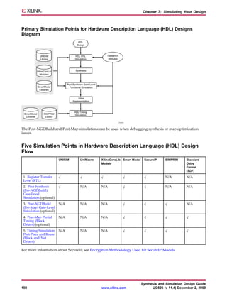
architecture BEHAVIORAL of async_fifo is
type ram_type is array ((2**FIFO_DEPTH)-1 downto 0) of std_logic_vector (FIFO_WIDTH-1 downto 0);
Verilog Parameter Coding Example
-- FIFO_WIDTH data width(number of bits)
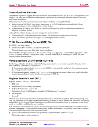
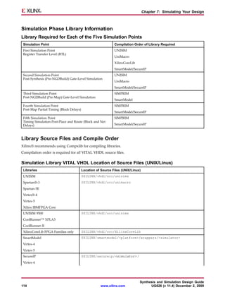
-- FIFO_DEPTH by number of address bits
-- for the FIFO RAM i.e. 9 -> 2**9 -> 512 words
-- FIFO_RAM_TYPE: BLOCKRAM or DISTRIBUTED_RAM
-- Note: DISTRIBUTED_RAM suggested for FIFO_DEPTH
-- of 5 or less
module async_fifo (din, rd_clk, rd_en, ainit, wr_clk, wr_en, dout, empty, full, almost_empty, almost_full, wr_ack);
parameter FIFO_WIDTH = 16;
parameter FIFO_DEPTH = 9;
parameter FIFO_RAM_TYPE = "BLOCKRAM";
input [FIFO_WIDTH-1:0] din;
input rd_clk;
input rd_en;
input ainit;
input wr_clk;
input wr_en;
output reg [FIFO_WIDTH-1:0] dout;
output empty;
output full;
output almost_empty;
output almost_full;
output reg wr_ack;
reg [FIFO_WIDTH-1:0] fifo_ram [(2**FIFO_DEPTH)-1:0];
TRANSLATE_OFF and TRANSLATE_ON
The synthesis directives TRANSLATE_OFF and TRANSLATE_ON were formerly used when passing generics
or parameters for synthesis tools, since most synthesis tools were unable to read generics or parameters.
These directives were also used for library declarations such as library UNISIM, since synthesis tools did not
understand that library.
Since most synthesis tools can now read generics and parameters and understand the UNISIM library, you no
longer need to use these directives in synthesizable code. TRANSLATE_OFF and TRANSLATE_ON can also be
used to embed simulation-only code in synthesizable files. Xilinx® recommends that any simulation-only
constructs reside in simulation-only files or test benches.
For more information about TRANSLATE_OFF and TRANSLATE_ON, see the Constraints Guide.
Synthesis and Simulation Design Guide
38 www.xilinx.com UG626 (v 11.4) December 2, 2009](https://image.slidesharecdn.com/sim-120220090038-phpapp01/85/Sim-38-320.jpg)
![Chapter 5: Coding for FPGA Device Flow
4–to–1 Multiplexer Design With If Statement Verilog Coding Example
/////////////////////////////////////////////////
// IF_EX.V //
// Example of a if statement showing a //
// mux created using priority encoded logic //
// HDL Synthesis Design Guide for FPGA devices //
/////////////////////////////////////////////////
module if_ex (
input A, B, C, D,
input [1:0] SEL,
output reg MUX_OUT);
always @ (*)
begin
if (SEL == 2’b00)
MUX_OUT = A;
else if (SEL == 2’b01)
MUX_OUT = B;
else if (SEL == 2’b10)
MUX_OUT = C;
else if (SEL == 2’b11)
MUX_OUT = D;
else
MUX_OUT = 0;
end
endmodule
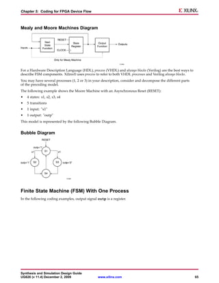
4–to–1 Multiplexer Design With Case Statement Coding Examples
The following coding examples use a case statement for the same multiplexer.
In these examples, the case statement requires only one slice, while the if statement requires two slices in some
synthesis tools. In this instance, design the multiplexer using the case statement. Fewer resources are used and
the delay path is shorter. When writing case statements, make sure all outputs are defined in all branches.
The Case_Ex Implementation diagram below shows the implementation of these designs.
4–to–1 Multiplexer Design With Case Statement VHDL Coding Example
-- CASE_EX.VHD
-- May 2001
library IEEE;
use IEEE.std_logic_1164.all;
use IEEE.std_logic_unsigned.all;
entity case_ex is
port (
SEL : in STD_LOGIC_VECTOR(1 downto 0);
A,B,C,D: in STD_LOGIC;
MUX_OUT: out STD_LOGIC);
end case_ex;
architecture BEHAV of case_ex is
begin
CASE_PRO: process (SEL,A,B,C,D)
begin
case SEL is
when “00” => MUX_OUT <= A;
when “01” => MUX_OUT <= B;
when “10” => MUX_OUT <= C;
when “11” => MUX_OUT <= D;
when others => MUX_OUT <= ’0’;
end case;
end process; --End CASE_PRO
end BEHAV;
Synthesis and Simulation Design Guide
UG626 (v 11.4) December 2, 2009 www.xilinx.com 47](https://image.slidesharecdn.com/sim-120220090038-phpapp01/85/Sim-47-320.jpg)
![Chapter 5: Coding for FPGA Device Flow
4–to–1 Multiplexer Design With Case Statement Verilog Coding Example
/////////////////////////////////////////////////
// CASE_EX.V //
// Example of a Case statement showing //
// A mux created using parallel logic //
// HDL Synthesis Design Guide for FPGA devices //
/////////////////////////////////////////////////
module case_ex (
input A, B, C, D,
input [1:0] SEL,
output reg MUX_OUT);
always @ (*)
begin
case (SEL)
2’b00: MUX_OUT = A;
2’b01: MUX_OUT = B;
2’b10: MUX_OUT = C;
2’b11: MUX_OUT = D;
default: MUX_OUT = 0;
endcase
end
endmodule
Case_Ex Implementation Diagram
Sensitivity List in Process and Always Statements
A sensitivity list in a process statement (VHDL) or always block (Verilog) is a list of signals to which the process
statement (VHDL) or always block (Verilog) is sensitive. When any of the listed signals changes its value, the
process statement (VHDL) or always block (Verilog) resumes and executes its statements. Depending on the
sensitivity list and set of statements, the process statement (VHDL) or always block (Verilog) can describe
sequential elements as flip-flops and latches or combinatorial elements, or a mix of them.
When working with sensitivity lists, be sure to specify all necessary signals. If you do not do so, hardware
generated from the Hardware Description Language (HDL) code may behave differently as compared to the
Register Transfer Level (RTL) description. This behavior arises from the synthesis tool for the following reasons:
• In some cases, it is impossible to model the RTL description using existing hardware.
• The HDL code requires additional logic in the final implementation in order to exactly model the RTL
description.
Synthesis and Simulation Design Guide
48 www.xilinx.com UG626 (v 11.4) December 2, 2009](https://image.slidesharecdn.com/sim-120220090038-phpapp01/85/Sim-48-320.jpg)
![Chapter 5: Coding for FPGA Device Flow
8-Bit Shift-Left Register Serial In and Serial Out Verilog Coding Example
module v_shift_regs_1 (C, SI, SO);
input C,SI;
output SO;
reg [7:0] tmp;
always @(posedge C)
begin
tmp = {tmp[6:0], SI};
end
assign SO = tmp[7];
endmodule
16-Bit Dynamic Shift Register With Serial In and Serial Out VHDL Coding Example
library IEEE;
use IEEE.std_logic_1164.all;
use IEEE.std_logic_unsigned.all;
entity dynamic_shift_regs_1 is
port(CLK : in std_logic;
DATA : in std_logic;
CE : in std_logic;
A : in std_logic_vector(3 downto 0);
Q : out std_logic);
end dynamic_shift_regs_1;
architecture rtl of dynamic_shift_regs_1 is
constant DEPTH_WIDTH : integer := 16;
type SRL_ARRAY is array (0 to DEPTH_WIDTH-1) of std_logic;
-- The type SRL_ARRAY can be array
-- (0 to DEPTH_WIDTH-1) of
-- std_logic_vector(BUS_WIDTH downto 0)
-- or array (DEPTH_WIDTH-1 downto 0) of
-- std_logic_vector(BUS_WIDTH downto 0)
-- (the subtype is forward (see below))
signal SRL_SIG : SRL_ARRAY;
begin
PROC_SRL16 : process (CLK)
begin
if (CLK’event and CLK = ’1’) then
if (CE = ’1’) then
SRL_SIG <= DATA & SRL_SIG(0 to DEPTH_WIDTH-2);
end if;
end if;
end process;
Q <= SRL_SIG(conv_integer(A));
end rtl;
16-Bit Dynamic Shift Register With Serial In and Serial Out Verilog Coding Example
module v_dynamic_shift_regs_1 (Q,CE,CLK,D,A);
input CLK, D, CE;
input [3:0] A;
output Q;
reg [15:0] data;
assign Q = data[A];
always @(posedge CLK)
begin
if (CE == 1’b1)
data <= {data[14:0], D};
end
endmodule
Synthesis and Simulation Design Guide
UG626 (v 11.4) December 2, 2009 www.xilinx.com 55](https://image.slidesharecdn.com/sim-120220090038-phpapp01/85/Sim-55-320.jpg)
![Chapter 5: Coding for FPGA Device Flow
Clock Enable VHDL Coding Example
library IEEE;
use IEEE.std_logic_1164.all;
use IEEE.std_logic_unsigned.all;
entity clock_enable is
port (DATA, IN1, IN2, LOAD, CLOCK: in STD_LOGIC;
OUT1: out STD_LOGIC);
end clock_enable;
architecture BEHAVIORAL of clock_enable is
signal ENABLE: std_logic;
begin
ENABLE <= IN1 and IN2 and LOAD;
EN_PR: process (CLOCK)
begin
if (CLOCK’event and CLOCK=’1’) then
if (ENABLE = ’1’) then
OUT1 <= DATA;
end if;
end if;
end process;
end BEHAVIORAL;
Clock Enable Verilog Coding Example
module clock_enable (
input DATA, IN1, IN2, LOAD, CLOCK,
output reg OUT1
);
wire ENABLE;
assign ENABLE = (IN1 & IN2 & LOAD);
always @(posedge CLOCK)
if (ENABLE)
OUT1 <= DATA;
endmoduleI
Implementation of Clock Enable Diagram
Initial State of the Registers and Latches
FPGA flip-flops are configured as either preset (asynchronous set) or clear (asynchronous reset) during startup.
This is known as the initialization state, or INIT. The initial state of the register can be specified as follows:
• If the register is instantiated, it can be specified by setting the INIT generic/parameter value to either a 1or 0,
depending on the desired state. For more information, see the Libraries Guides.
• If the register is inferred, the initial state can be specified by initializing the VHDL signal declaration or the
Verilog reg declaration as shown in the following coding examples.
Initial State of the Registers and Latches VHDL Coding Example One
signal register1 : std_logic := ’0’; -- specifying register1 to start as a zero
signal register2 : std_logic := ’1’; -- specifying register2 to start as a one
signal register3 : std_logic_vector(3 downto 0):="1011"; -- specifying INIT value for 4-bit register
Initial State of the Registers and Latches Verilog Coding Example One
reg register1 = 1’b0; // specifying regsiter1 to start as a zero
reg register2 = 1’b1; // specifying register2 to start as a one
reg [3:0] register3 = 4’b1011; //specifying INIT value for 4-bit register
Synthesis and Simulation Design Guide
UG626 (v 11.4) December 2, 2009 www.xilinx.com 61](https://image.slidesharecdn.com/sim-120220090038-phpapp01/85/Sim-61-320.jpg)
![Chapter 5: Coding for FPGA Device Flow
Initial State of the Registers and Latches Verilog Coding Example Two
Another possibility in Verilog is to use an initial statement:
reg [3:0] register3;
initial begin
register3= 4’b1011;
end
Not all synthesis tools support this initialization. To determine whether it is supported, see your synthesis
tool documentation. If this initialization is not supported, or if it is not specified in the code, the initial value
is determined by the presence or absence of an asynchronous preset in the code. If an asynchronous preset is
present, the register initializes to a one. If an asynchronous preset is not present, the register initializes to a
logic zero.
Initial State of the Shift Registers
The definition method of initial values for shift registers is the same used for Registers and Latches. For more
information, see Initial State of the Registers and Latches.
Initial State of the RAMs
The definition method of initial values for RAMs (block or distributed) is similar to the one used for Registers
and Latches. The initial state of the RAM can be specified as follows:
• If the RAM is instantiated, it can be specified by setting the INIT_00, INIT_01, … generic/parameter values,
depending on the desired state. For more information, see the Libraries Guides.
• If the RAM is inferred, the initial state can be specified by initializing the VHDL signal declaration or using
Verilog initial statement as shown in the following coding examples. The initial values could be specified
directly in the HDL code, or in an external file containing the initialization data.
Initial State of the RAMs VHDL Coding Example
type ram_type is array (0 to 63) of std_logic_vector(19 downto 0);
signal RAM : ram_type :=(
X"0200A", X"00300", X"08101", X"04000", X"08601", X"0233A",
X"00300", X"08602", X"02310", X"0203B", X"08300", X"04002",
X"08201", X"00500", ... );
Initial State of the RAMs Verilog Coding Example
reg [19:0] ram [63:0];
initial begin
ram[63] = 20’h0200A; ram[62] = 20’h00300; ram[61] = 20’h08101;
ram[60] = 20’h04000; ram[59] = 20’h08601; ram[58] = 20’h0233A;
...
ram[2] = 20’h02341; ram[1] = 20’h08201; ram[0] = 20’h0400D;
end
Not all synthesis tools support this initialization. To determine whether it is supported, see your synthesis
tool documentation.
Multiplexers
You can implement multiplexers on Xilinx® FPGA devices by using:
• Dedicated resources such as MUXF5, MUXF6 ...
• Using Carry chains
• LUTs only
The implementation choice is automatically taken by the synthesis tool and driven by speed or area design
requirements. However some synthesis tools allow you to control the implementation style of multiplexers.
Synthesis and Simulation Design Guide
62 www.xilinx.com UG626 (v 11.4) December 2, 2009](https://image.slidesharecdn.com/sim-120220090038-phpapp01/85/Sim-62-320.jpg)
![Chapter 5: Coding for FPGA Device Flow
For more information, see your synthesis tool documentation.
There are different description styles for multiplexers (MUXs), such as If-Then-Else or Case. When writing
MUXs, pay special attention in order to avoid common traps. For example, if you describe a MUX using a Case
statement, and you do not specify all values of the selector, the result may be latches instead of a multiplexer.
Verilog Case statements can be:
• full
• not full
A Case statement is full if all possible branches are specified.
Verilog Case statements can also be:
• parallel
• not parallel
A Case statement is parallel if it does not contain branches that can be executed simultaneously.
Synthesis tools automatically determine the characteristics of the Case statements and generate corresponding
logic. In addition they provide a way of allowing guide interpretation of Case statements by means of special
directives.
For more information, see your synthesis tool documentation.
4-to-1 1-Bit MUX Using Case Statement VHDL Coding Example
library ieee;
use ieee.std_logic_1164.all;
entity multiplexers_2 is
port (a, b, c, d : in std_logic;
s : in std_logic_vector (1 downto 0);
o : out std_logic);
end multiplexers_2;
architecture archi of multiplexers_2 is
begin
process (a, b, c, d, s)
begin
case s is
when "00" => o <= a;
when "01" => o <= b;
when "10" => o <= c;
when others => o <= d;
end case;
end process;
end archi;
4-to-1 1-Bit MUX Using Case Statement Verilog Coding Example
module v_mults_2 (a, b, c, d, s, o);
input a,b,c,d;
input [1:0] s;
output o;
reg o;
always @(a or b or c or d or s)
begin
case (s)
2’b00 : o = a;
2’b01 : o = b;
2’b10 : o = c;
default : o = d;
endcase
end
endmodule
Synthesis and Simulation Design Guide
UG626 (v 11.4) December 2, 2009 www.xilinx.com 63](https://image.slidesharecdn.com/sim-120220090038-phpapp01/85/Sim-63-320.jpg)
![Chapter 5: Coding for FPGA Device Flow
4-to-1 1-Bit MUX Using IF Statement VHDL Coding Example
library ieee;
use ieee.std_logic_1164.all;
entity multiplexers_1 is
port (a, b, c, d : in std_logic;
s : in std_logic_vector (1 downto 0);
o : out std_logic);
end multiplexers_1;
architecture archi of multiplexers_1 is
begin
process (a, b, c, d, s)
begin
if (s = "00") then o <= a;
elsif (s = "01") then o <= b;
elsif (s = "10") then o <= c;
else o <= d;
end if;
end process;
end archi;
4-to-1 1-Bit MUX Using IF Statement Verilog Coding Example
module v_mults_1 (a, b, c, d, s, o);
input a,b,c,d;
input [1:0] s;
output o;
reg o;
always @(a or b or c or d or s)
begin
if (s == 2’b00) o = a;
else if (s == 2’b01) o = b;
else if (s == 2’b10) o = c;
else o = d;
end
endmodule
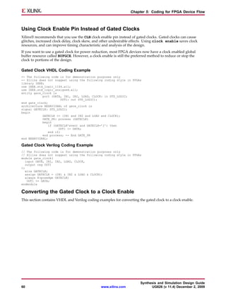
Finite State Machine (FSM) Components
This section discusses Finite State Machine (FSM) Components, and includes:
• Finite State Machine (FSM) Description Style
• Finite State Machine (FSM) With One Process
• Finite State Machine (FSM) With Two or Three Processes
• Finite State Machine (FSM) Recognition and Optimization
• Other Finite State Machine (FSM) Features
Finite State Machine (FSM) Description Style
Most FPGA synthesis tools propose a large set of templates to describe a Finite State Machine (FSM). There are
many ways to describe FSM components. A traditional FSM representation incorporates Mealy and Moore
machines, as shown in the following diagram.
Synthesis and Simulation Design Guide
64 www.xilinx.com UG626 (v 11.4) December 2, 2009](https://image.slidesharecdn.com/sim-120220090038-phpapp01/85/Sim-64-320.jpg)
![Chapter 5: Coding for FPGA Device Flow
Finite State Machine (FSM) With a Single Always Block Verilog Coding Example
//
// State Machine with a single always block.
//
module v_fsm_1 (clk, reset, x1, outp);
input clk, reset, x1;
output outp;
reg outp;
reg [1:0] state;
parameter s1 = 2’b00; parameter s2 = 2’b01;
parameter s3 = 2’b10; parameter s4 = 2’b11;
initial begin
state = 2’b00;
end
always@(posedge clk or posedge reset)
begin
if (reset)
begin
state <= s1; outp <= 1’b1;
end
else
begin
case (state)
s1: begin
if (x1==1’b1)
begin
state <= s2;
outp <= 1’b1;
end
else
begin
state <= s3;
outp <= 1’b0;
end
end
s2: begin
state <= s4; outp <= 1’b1;
end
s3: begin
state <= s4; outp <= 1’b0;
end
s4: begin
state <= s1; outp <= 1’b0;
end
endcase
end
end
endmodule
In VHDL, the type of a state register can be a different type, such as:
• integer
• bit_vector
• std_logic_vector
Xilinx® recommends that you use an enumerated type containing all possible state values and to declare your
state register with that type. This method was used in the previous VHDL Coding Example.
In Verilog, the type of state register can be an integer or a set of defined parameters. Xilinx recommends using a
set of defined for state register definition. This method was used in the previous Verilog coding example.
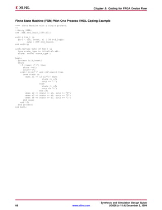
Finite State Machine (FSM) With Two or Three Processes
A Finite State Machine (FSM) With One Process can be described with two processes using the FSM
decomposition shown in the following diagram.
Synthesis and Simulation Design Guide
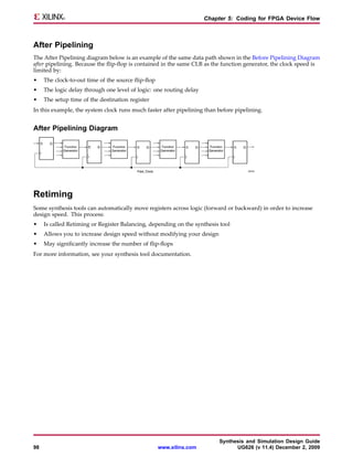
UG626 (v 11.4) December 2, 2009 www.xilinx.com 67](https://image.slidesharecdn.com/sim-120220090038-phpapp01/85/Sim-67-320.jpg)
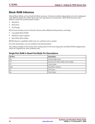
![Chapter 5: Coding for FPGA Device Flow
Single-Port RAM in Read-First Mode VHDL Coding Example
library ieee;
use ieee.std_logic_1164.all;
use ieee.std_logic_unsigned.all;
entity rams_01 is
port (clk : in std_logic;
we : in std_logic;
en : in std_logic;
addr : in std_logic_vector(5 downto 0);
di : in std_logic_vector(15 downto 0);
do : out std_logic_vector(15 downto 0));
end rams_01;
architecture syn of rams_01 is
type ram_type is array (63 downto 0) of std_logic_vector (15 downto 0);
signal RAM: ram_type;
begin
process (clk)
begin
if clk’event and clk = ’1’ then
if en = ’1’ then
if we = ’1’ then
RAM(conv_integer(addr)) <= di;
end if;
do <= RAM(conv_integer(addr)) ;
end if;
end if;
end process;
end syn;
Single-Port RAM in Read-First Mode Verilog Coding Example
module v_rams_01 (clk, en, we, addr, di, do);
input clk;
input we;
input en;
input [5:0] addr;
input [15:0] di;
output [15:0] do;
reg [15:0] RAM [63:0];
reg [15:0] do;
always @(posedge clk)
begin
if (en)
begin
if (we)
RAM[addr]<=di;
do <= RAM[addr];
end
end
endmodule
Single-Port RAM in Write-First Mode Pin Descriptions
IO Pins Description
clk Positive-Edge Clock
we Synchronous Write Enable (Active High)
en Clock Enable
addr Read/Write Address
di Data Input
do Data Output
Synthesis and Simulation Design Guide
UG626 (v 11.4) December 2, 2009 www.xilinx.com 71](https://image.slidesharecdn.com/sim-120220090038-phpapp01/85/Sim-71-320.jpg)
![Chapter 5: Coding for FPGA Device Flow
Single-Port RAM in Write-First Mode VHDL Coding Example One
library ieee;
use ieee.std_logic_1164.all;
use ieee.std_logic_unsigned.all;
entity rams_02a is
port (clk : in std_logic;
we : in std_logic;
en : in std_logic;
addr : in std_logic_vector(5 downto 0);
di : in std_logic_vector(15 downto 0);
do : out std_logic_vector(15 downto 0));
end rams_02a;
architecture syn of rams_02a is
type ram_type is array (63 downto 0)
of std_logic_vector (15 downto 0);
signal RAM : ram_type;
begin
process (clk)
begin
if clk’event and clk = ’1’ then
if en = ’1’ then
if we = ’1’ then
RAM(conv_integer(addr)) <= di;
do <= di;
else
do <= RAM( conv_integer(addr));
end if;
end if;
end if;
end process;
end syn;
Single-Port RAM in Write-First Mode Verilog Coding Example One
module v_rams_02a (clk, we, en, addr, di, do);
input clk;
input we;
input en;
input [5:0] addr;
input [15:0] di;
output [15:0] do;
reg [15:0] RAM [63:0];
reg [15:0] do;
always @(posedge clk)
begin
if (en)
begin
if (we)
begin
RAM[addr] <= di;
do <= di;
end
else
do <= RAM[addr];
end
end
endmodule
Synthesis and Simulation Design Guide
72 www.xilinx.com UG626 (v 11.4) December 2, 2009](https://image.slidesharecdn.com/sim-120220090038-phpapp01/85/Sim-72-320.jpg)
![Chapter 5: Coding for FPGA Device Flow
Single-Port RAM in Write-First Mode VHDL Coding Example Two
library ieee;
use ieee.std_logic_1164.all;
use ieee.std_logic_unsigned.all;
entity rams_02b is
port (clk : in std_logic;
we : in std_logic;
en : in std_logic;
addr : in std_logic_vector(5 downto 0);
di : in std_logic_vector(15 downto 0);
do : out std_logic_vector(15 downto 0));
end rams_02b;
architecture syn of rams_02b is
type ram_type is array (63 downto 0) of std_logic_vector (15 downto 0);
signal RAM : ram_type;
signal read_addr: std_logic_vector(5 downto 0);
begin
process (clk)
begin
if clk’event and clk = ’1’ then
if en = ’1’ then
if we = ’1’ then
ram(conv_integer(addr)) <= di;
end if;
read_addr <= addr;
end if;
end if;
end process;
do <= ram(conv_integer(read_addr));
end syn;
Single-Port RAM in Write-First Mode Verilog Coding Example Two
module v_rams_02b (clk, we, en, addr, di, do);
input clk;
input we;
input en;
input [5:0] addr;
input [15:0] di;
output [15:0] do;
reg [15:0] RAM [63:0];
reg [5:0] read_addr;
always @(posedge clk)
begin
if (en)
begin
if (we)
RAM[addr] <= di;
read_addr <= addr;
end
end
assign do = RAM[read_addr];
endmodule
Synthesis and Simulation Design Guide
UG626 (v 11.4) December 2, 2009 www.xilinx.com 73](https://image.slidesharecdn.com/sim-120220090038-phpapp01/85/Sim-73-320.jpg)
![Chapter 5: Coding for FPGA Device Flow
Single-Port RAM In No-Change Mode Verilog Coding Example
module v_rams_03 (clk, we, en, addr, di, do);
input clk;
input we;
input en;
input [5:0] addr;
input [15:0] di;
output [15:0] do;
reg [15:0] RAM [63:0];
reg [15:0] do;
always @(posedge clk)
begin
if (en)
begin
if (we)
RAM[addr] <= di;
else
do <= RAM[addr];
end
end
endmodule
Dual-Port RAM in Read-First Mode With One Write Port Pin Descriptions
IO Pins Description
clka, clkb Positive-Edge Clock
ena Primary Global Enable (Active High)
enb Dual Global Enable (Active High)
wea Primary Synchronous Write
addra Write Address/Primary Read Address
addrb Dual Read Address
dia Primary Data Input
doa Primary Output Port
dob Dual Output Port
Synthesis and Simulation Design Guide
UG626 (v 11.4) December 2, 2009 www.xilinx.com 75](https://image.slidesharecdn.com/sim-120220090038-phpapp01/85/Sim-75-320.jpg)
![Chapter 5: Coding for FPGA Device Flow
Dual-Port RAM in Read-First Mode with One Write Port Verilog Coding Example
module v_rams_01_1 (clka, clkb, ena, enb, wea, addra, addrb, dia, doa, dob);
input clka, clkb;
input wea;
input ena, enb;
input [5:0] addra, addrb;
input [15:0] dia;
output [15:0] doa, dob;
reg [15:0] RAM [63:0];
reg [15:0] doa, dob;
always @(posedge clka)
begin
if (ena)
begin
if (wea)
RAM[addra]<=dia;
doa <= RAM[addra];
end
end
always @(posedge clkb)
begin
if (enb)
begin
dob <= RAM[addrb];
end
end
endmodule
Dual-Port Block RAM in Read-First Mode With Two Write Ports
Some synthesis tools support dual-port block RAMs with two write ports for VHDL and Verilog. The concept of
dual-write ports implies not only distinct data ports, but also the possibility of having distinct write clocks and
write enables. Distinct write clocks also mean distinct read clocks, since the dual-port block RAM offers two
clocks, one shared by the primary read and write port, the other shared by the secondary read and write port. In
VHDL, the description of this type of block RAM is based on the usage of shared variables.
Because of the shared variable, the description of the different read/write synchronizations may be different from
coding examples recommended for single-write RAMs. The order of appearance of the different lines of code
is significant. In the next VHDL example describing read-first synchronization the read statement must come
BEFORE the write statement.
Dual-Port Block RAM in Read-First Mode With Two Write Ports Pin Descriptions
IO Pins Description
clka, clkb Positive-Edge Clock
ena Primary Global Enable (Active High)
enb Dual Global Enable (Active High)
wea, web Primary Synchronous Write Enable (Active High)
addra Write Address/Primary Read Address
addrb Dual Read Address
dia Primary Data Input
dib Dual Data Input
doa Primary Output Port
dob Dual Output Port
Synthesis and Simulation Design Guide
UG626 (v 11.4) December 2, 2009 www.xilinx.com 77](https://image.slidesharecdn.com/sim-120220090038-phpapp01/85/Sim-77-320.jpg)
![Chapter 5: Coding for FPGA Device Flow
Dual-Port Block RAM in Read-First Mode With Two Write Ports Verilog Coding Example
module v_rams_16 (clka,clkb,ena,enb,wea,web,addra,addrb,dia,dib,doa,dob);
input clka,clkb,ena,enb,wea,web;
input [5:0] addra,addrb;
input [15:0] dia,dib;
output [15:0] doa,dob;
reg [15:0] ram [63:0];
reg [15:0] doa,dob;
always @(posedge clka) begin
if (ena)
begin
if (wea)
ram[addra] <= dia;
doa <= ram[addra];
end
end
always @(posedge clkb) begin
if (enb)
begin
if (web)
ram[addrb] <= dib;
dob <= ram[addrb];
end
end
endmodule
Distributed RAM Inference
The coding examples shown below provide coding styles for the most frequently used Distributed RAM
configurations, which are supported by most synthesis tools.
Single-Port Distributed RAM Pin Descriptions
IO Pins Description
clk Positive-Edge Clock
we Synchronous Write Enable (Active High)
a Read/Write Address
di Data Input
do Data Output
Synthesis and Simulation Design Guide
UG626 (v 11.4) December 2, 2009 www.xilinx.com 79](https://image.slidesharecdn.com/sim-120220090038-phpapp01/85/Sim-79-320.jpg)
![Chapter 5: Coding for FPGA Device Flow
Single-Port Distributed RAM VHDL Coding Example
library ieee;
use ieee.std_logic_1164.all;
use ieee.std_logic_unsigned.all;
entity rams_04 is
port (clk : in std_logic;
we : in std_logic;
a : in std_logic_vector(5 downto 0);
di : in std_logic_vector(15 downto 0);
do : out std_logic_vector(15 downto 0));
end rams_04;
architecture syn of rams_04 is
type ram_type is array (63 downto 0) of std_logic_vector (15 downto 0);
signal RAM : ram_type;
begin
process (clk)
begin
if (clk’event and clk = ’1’) then
if (we = ’1’) then
RAM(conv_integer(a)) <= di;
end if;
end if;
end process;
do <= RAM(conv_integer(a));
end syn;
Single-Port Distributed RAM Verilog Coding Example
module v_rams_04 (clk, we, a, di, do);
input clk;
input we;
input [5:0] a;
input [15:0] di;
output [15:0] do;
reg [15:0] ram [63:0];
always @(posedge clk) begin
if (we)
ram[a] <= di;
end
assign do = ram[a];
endmodule
Dual-Port Distributed RAM Pin Descriptions
IO Pins Description
clk Positive-Edge Clock
we Synchronous Write Enable (Active High)
a Write Address/Primary Read Address
dpra Dual Read Address
di Data Input
spo Primary Output Port
dpo Dual Output Port
Synthesis and Simulation Design Guide
80 www.xilinx.com UG626 (v 11.4) December 2, 2009](https://image.slidesharecdn.com/sim-120220090038-phpapp01/85/Sim-80-320.jpg)
![Chapter 5: Coding for FPGA Device Flow
Dual-Port Distributed RAM VHDL Coding Example
library ieee;
use ieee.std_logic_1164.all;
use ieee.std_logic_unsigned.all;
entity rams_09 is
port (clk : in std_logic;
we : in std_logic;
a : in std_logic_vector(5 downto 0);
dpra : in std_logic_vector(5 downto 0);
di : in std_logic_vector(15 downto 0);
spo : out std_logic_vector(15 downto 0);
dpo : out std_logic_vector(15 downto 0));
end rams_09;
architecture syn of rams_09 is
type ram_type is array (63 downto 0) of std_logic_vector (15 downto 0);
signal RAM : ram_type;
begin
process (clk)
begin
if (clk’event and clk = ’1’) then
if (we = ’1’) then
RAM(conv_integer(a)) <= di;
end if;
end if;
end process;
spo <= RAM(conv_integer(a));
dpo <= RAM(conv_integer(dpra));
end syn;
Dual-Port Distributed RAM Verilog Coding Example
module v_rams_09 (clk, we, a, dpra, di, spo, dpo);
input clk;
input we;
input [5:0] a;
input [5:0] dpra;
input [15:0] di;
output [15:0] spo;
output [15:0] dpo;
reg [15:0] ram [63:0];
always @(posedge clk) begin
if (we)
ram[a] <= di;
end
assign spo = ram[a];
assign dpo = ram[dpra];
endmodule
Arithmetic Support
Xilinx® FPGA devices traditionally contain several hardware resources such as LUTs and Carry Chains. These
hardware resources efficiently implement various arithmetic operations such as adders, subtractors, counters,
accumulators, and comparators.
With the release of the Virtex®-4 device, Xilinx introduced a new primitive called DSP48. This block was
further enhanced in later families such as Virtex-5 devices and Spartan®-3A DSP devices. DSP48 allows you to
create numerous functions, including multipliers, adders, counters, barrel shifters, comparators, accumulators,
multiply accumulate, complex multipliers, and others.
Synthesis and Simulation Design Guide
UG626 (v 11.4) December 2, 2009 www.xilinx.com 81](https://image.slidesharecdn.com/sim-120220090038-phpapp01/85/Sim-81-320.jpg)
![Chapter 5: Coding for FPGA Device Flow
Currently, synthesis tools support the most important and frequently used DSP48 modes for DSP applications
such as multipliers, adders/subtractors, multiply adders/subtractors, and multiply accumulate. The synthesis
tools also take advantage of the internal registers available in DSP48, as well as the dynamic OPMODE port.
DSP48 fast connections allow you to efficiently build fast DSP48 chains as filters. These fast connections are
automatically supported by synthesis tools today.
The level of DSP48 support may differ from one synthesis tool to another.
For more information, see your synthesis tool documentation.
Since there are several ways to implement the same arithmetic operation on the target device, synthesis tools
make automatic choices depending on the operation type, size, context usage, or timing requirements. In some
situations, the automatic choice may not meet your goals. Synthesis tools therefore offer several constraints to
control implementation process such as use_dsp48 in Xilinx Synthesis Technology (XST) or syn_dspstyle in
Synplicity.
For more information, see your synthesis tool documentation.
If you migrate a design previously implemented using an older and FPGA device family to a newer one with a
DSP48 block, and you want to take advantage of available DSP48 blocks, you must be aware of the following
rules in order to get the best performance.
• DSP48 blocks give you the best performance when fully pipelined. You should add additional pipelining
stages in order to get the best performance.
• Internal DSP48 registers support synchronous set and reset signals. Asynchronous set and reset signals are
not supported. You must replace asynchronous initialization signals by synchronous ones. Some synthesis
tools may automatically make this replacement. This operation renders the generated netlist NOT equivalent
to the initial RTL description.
For more information, see your synthesis tool documentation.
• For DSP applications, use chain structures instead of tree structures in your RTL description in order to take
full advantage of the DSP48 capabilities.
For more information on DSP48 blocks and specific DSP application coding style, see the XtremeDSP™ User
Guide for your target family.
Unsigned 8-bit Adder VHDL Coding Example
library ieee;
use ieee.std_logic_1164.all;
use ieee.std_logic_unsigned.all;
entity arith_01 is
port(A,B : in std_logic_vector(7 downto 0);
SUM : out std_logic_vector(7 downto 0));
end arith_01;
architecture archi of arith_01 is
begin
SUM <= A + B;
end archi;
Unsigned 8-bit Adder Verilog Coding Example
module v_arith_01(A, B, SUM);
input [7:0] A;
input [7:0] B;
output [7:0] SUM;
assign SUM = A + B;
Endmodule
Synthesis and Simulation Design Guide
82 www.xilinx.com UG626 (v 11.4) December 2, 2009](https://image.slidesharecdn.com/sim-120220090038-phpapp01/85/Sim-82-320.jpg)
![Chapter 5: Coding for FPGA Device Flow
Signed 8-bit Adder VHDL Coding Example
library ieee;
use ieee.std_logic_1164.all;
use ieee.std_logic_signed.all;
entity arith_02 is
port(A,B : in std_logic_vector(7 downto 0);
SUM : out std_logic_vector(7 downto 0));
end arith_02;
architecture archi of arith_02 is
begin
SUM <= A + B;
end archi;
Signed 8-bit Adder Verilog Coding Example
module v_arith_02 (A,B,SUM);
input signed [7:0] A;
input signed [7:0] B;
output signed [7:0] SUM;
wire signed [7:0] SUM;
assign SUM = A + B;
Endmodule
Unsigned 8-bit Adder with Registered Input/Outputs VHDL Coding Example
library ieee;
use ieee.std_logic_1164.all;
use ieee.std_logic_unsigned.all;
entity arith_03 is
port(clk : in std_logic;
A,B : in std_logic_vector(7 downto 0);
SUM : out std_logic_vector(7 downto 0));
end arith_03;
architecture archi of arith_03 is
signal reg_a, reg_b: std_logic_vector(7 downto 0);
begin
process (clk)
begin
if (clk’event and clk=’1’) then
reg_a <= A;
reg_b <= B;
SUM <= reg_a + reg_b;
end if;
end process;
end archi;
Synthesis and Simulation Design Guide
UG626 (v 11.4) December 2, 2009 www.xilinx.com 83](https://image.slidesharecdn.com/sim-120220090038-phpapp01/85/Sim-83-320.jpg)
![Chapter 5: Coding for FPGA Device Flow
Unsigned 8-bit Adder with Registered Input/Outputs Verilog Coding Example
module v_arith_03 (clk, A, B, SUM);
input clk;
input [7:0] A;
input [7:0] B;
output [7:0] SUM;
reg [7:0] reg_a, reg_b, SUM;
always @(posedge clk)
begin
reg_a <= A;
reg_b <= B;
SUM <= reg_a + reg_b;
end
endmodule
Unsigned 8-bit Adder/Subtractor VHDL Coding Example
library ieee;
use ieee.std_logic_1164.all;
use ieee.std_logic_unsigned.all;
entity arith_04 is
port(A,B : in std_logic_vector(7 downto 0);
OPER: in std_logic;
RES : out std_logic_vector(7 downto 0));
end arith_04;
architecture archi of arith_04 is
begin
RES <= A + B when OPER=’0’
else A - B;
end archi;
Unsigned 8-bit Adder/Subtractor Verilog Coding Example
module v_arith_04 (A, B, OPER, RES);
input OPER;
input [7:0] A;
input [7:0] B;
output [7:0] RES;
reg [7:0] RES;
always @(A or B or OPER)
begin
if (OPER==1’b0) RES = A + B;
else RES = A - B;
end
endmodule
Unsigned 8-Bit Greater or Equal Comparator VHDL Coding Example
library ieee;
use ieee.std_logic_1164.all;
use ieee.std_logic_unsigned.all;
entity arith_05 is
port(A,B : in std_logic_vector(7 downto 0);
CMP : out std_logic);
end arith_05;
architecture archi of arith_05 is
begin
CMP <= ’1’ when A >= B else ’0’;
end archi;
Synthesis and Simulation Design Guide
84 www.xilinx.com UG626 (v 11.4) December 2, 2009](https://image.slidesharecdn.com/sim-120220090038-phpapp01/85/Sim-84-320.jpg)
![Chapter 5: Coding for FPGA Device Flow
Unsigned 8-Bit Greater or Equal Comparator Verilog Coding Example
module v_arith_05 (A, B, CMP);
input [7:0] A;
input [7:0] B;
output CMP;
assign CMP = (A >= B) ? 1’b1 : 1’b0;
endmodule
Unsigned 17x17-Bit Multiplier with Registered Input/Outputs VHDL Coding Example
library ieee;
use ieee.std_logic_1164.all;
use ieee.numeric_std.all;
entity arith_06 is
port(clk : in std_logic;
A : in unsigned (16 downto 0);
B : in unsigned (16 downto 0);
MULT : out unsigned (33 downto 0));
end arith_06;
architecture beh of arith_06 is
signal reg_a, reg_b : unsigned (16 downto 0);
begin
process (clk)
begin
if (clk’event and clk=’1’) then
reg_a <= A; reg_b <= B;
MULT <= reg_a * reg_b;
end if;
end process;
end beh;
Unsigned 17x17-Bit Multiplier with Registered Input/Outputs Verilog Coding Example
module v_arith_06(clk, A, B, MULT);
input clk;
input [16:0] A;
input [16:0] B;
output [33:0] MULT;
reg [33:0] MULT;
reg [16:0] reg_a, reg_b;
always @(posedge clk)
begin
reg_a <= A;
reg_b <= B;
MULT <= reg_a * reg_b;
end
endmodule
Synthesis and Simulation Design Guide
UG626 (v 11.4) December 2, 2009 www.xilinx.com 85](https://image.slidesharecdn.com/sim-120220090038-phpapp01/85/Sim-85-320.jpg)
![Chapter 5: Coding for FPGA Device Flow
Unsigned 8-Bit Up Counter with an Synchronous Reset VHDL Coding Example
library ieee;
use ieee.std_logic_1164.all;
use ieee.std_logic_unsigned.all;
entity arith_07 is
port(clk, reset : in std_logic;
Res : out std_logic_vector(7 downto 0));
end arith_07;
architecture archi of arith_07 is
signal cnt: std_logic_vector(7 downto 0);
begin
process (clk)
begin
if (clk’event and clk=’1’) then
if (reset = ’1’) then
cnt <= "00000000";
else
cnt <= cnt + 1;
end if;
end if;
end process;
Res <= cnt;
end archi;
Unsigned 8-Bit Up Counter with an Synchronous Reset Verilog Coding Example
module v_arith_07 (clk, reset, Res);
input clk, reset;
output [7:0] Res;
reg [7:0] cnt;
always @(posedge clk)
begin
if (reset)
cnt <= 8’b00000000;
else
cnt <= cnt + 1’b1;
end
assign Res = cnt;
endmodule
Synthesis and Simulation Design Guide
86 www.xilinx.com UG626 (v 11.4) December 2, 2009](https://image.slidesharecdn.com/sim-120220090038-phpapp01/85/Sim-86-320.jpg)
![Chapter 5: Coding for FPGA Device Flow
Unsigned 8-Bit Up Accumulator With Synchronous Reset VHDL Coding Example
library ieee;
use ieee.std_logic_1164.all;
use ieee.std_logic_unsigned.all;
entity arith_08 is
port(clk, reset : in std_logic;
din : in std_logic_vector(7 downto 0);
Res : out std_logic_vector(7 downto 0));
end arith_08;
architecture archi of arith_08 is
signal accu: std_logic_vector(7 downto 0);
begin
process (clk)
begin
if (clk’event and clk=’1’) then
if (reset = ’1’) then
accu <= "00000000";
else
accu <= accu + din;
end if;
end if;
end process;
Res <= accu;
end archi;
Unsigned 8-Bit Up Accumulator With Synchronous Reset Verilog Coding Example
module v_arith_08 (clk, reset, din, Res);
input clk, reset;
input [7:0] din;
output [7:0] Res;
reg [7:0] accu;
always @(posedge clk)
begin
if (reset)
accu <= 8’b00000000;
else
accu <= accu + din;
end
assign Res = accu;
endmodule
Synthesis and Simulation Design Guide
UG626 (v 11.4) December 2, 2009 www.xilinx.com 87](https://image.slidesharecdn.com/sim-120220090038-phpapp01/85/Sim-87-320.jpg)
![Chapter 5: Coding for FPGA Device Flow
Multiplier Adder With 2 Register Levels on Multiplier Inputs, 1 Register Level after Multiplier and
1 Register Level after Adder VHDL Coding Example
library IEEE;
use IEEE.STD_LOGIC_1164.ALL;
use IEEE.STD_LOGIC_UNSIGNED.ALL;
entity arith_09 is
generic (p_width: integer:=8);
port (clk : in std_logic;
A, B : in std_logic_vector(7 downto 0);
C : in std_logic_vector(15 downto 0);
RES : out std_logic_vector(15 downto 0));
end arith_09;
architecture beh of arith_09 is
signal reg1_A, reg2_A,
reg1_B, reg2_B : std_logic_vector(7 downto 0);
signal reg_C, reg_mult : std_logic_vector(15 downto 0);
begin
process (clk)
begin
if (clk’event and clk=’1’) then
reg1_A <= A; reg2_A <= reg1_A;
reg1_B <= B; reg2_B <= reg1_B;
reg_C <= C;
reg_mult <= reg2_A * reg2_B;
RES <= reg_mult + reg_C;
end if;
end process;
end beh;
Multiplier Adder With 2 Register Levels on Multiplier Inputs, 1 Register Level after Multiplier and
1 Register Level after Adder Verilog Coding Example
module v_arith_09 (clk, A, B, C, RES);
input clk;
input [7:0] A;
input [7:0] B;
input [15:0] C;
output [15:0] RES;
reg [7:0] reg1_A, reg2_A, reg1_B, reg2_B;
reg [15:0] reg_C, reg_mult, RES;
always @(posedge clk)
begin
reg1_A <= A; reg2_A <= reg1_A;
reg1_B <= B; reg2_B <= reg1_B;
reg_C <= C;
reg_mult <= reg2_A * reg2_B;
RES <= reg_mult + reg_C;
end
endmodule
Synthesis and Simulation Design Guide
88 www.xilinx.com UG626 (v 11.4) December 2, 2009](https://image.slidesharecdn.com/sim-120220090038-phpapp01/85/Sim-88-320.jpg)
![Chapter 5: Coding for FPGA Device Flow
Multiplier Up Accumulator With 2 Register Levels on Multiplier Inputs, 1 Register Level after
Multiplier and 1 Register Level after Accumulator VHDL Coding Example
library IEEE;
use IEEE.STD_LOGIC_1164.ALL;
use IEEE.STD_LOGIC_UNSIGNED.ALL;
entity arith_10 is
port (clk : in std_logic;
A, B : in std_logic_vector(7 downto 0);
RES : out std_logic_vector(15 downto 0));
end arith_10;
architecture beh of arith_10 is
signal reg1_A, reg2_A,
reg1_B, reg2_B : std_logic_vector(7 downto 0);
signal reg_mult, reg_accu : std_logic_vector(15 downto 0);
begin
process (clk)
begin
if (clk’event and clk=’1’) then
reg1_A <= A; reg2_A <= reg1_A;
reg1_B <= B; reg2_B <= reg1_B;
reg_mult <= reg2_A * reg2_B;
reg_accu <= reg_accu + reg_mult;
end if;
end process;
RES <= reg_accu;
end beh;
Multiplier Up Accumulator With 2 Register Levels on Multiplier Inputs, 1 Register Level after
Multiplier and 1 Register Level after Accumulator Verilog Coding Example
module v_arith_10 (clk, A, B, RES);
input clk;
input [7:0] A;
input [7:0] B;
output [15:0] RES;
reg [7:0] reg1_A, reg2_A, reg1_B, reg2_B;
reg [15:0] reg_mult, reg_accu;
wire [15:0] RES;
always @(posedge clk)
begin
reg1_A <= A; reg2_A <= reg1_A;
reg1_B <= B; reg2_B <= reg1_B;
reg_mult <= reg2_A * reg2_B;
reg_accu <= reg_accu + reg_mult;
end
assign RES = reg_accu;
endmodule
Order and Group Arithmetic Functions
The ordering and grouping of arithmetic functions can influence design performance. For example, the following
two VHDL statements are not necessarily equivalent:
ADD <= A1 + A2 + A3 + A4;
ADD <= (A1 + A2) + (A3 + A4);
For Verilog, the following two statements are not necessarily equivalent:
ADD = A1 + A2 + A3 + A4;
ADD = (A1 + A2) + (A3 + A4);
Synthesis and Simulation Design Guide
UG626 (v 11.4) December 2, 2009 www.xilinx.com 89](https://image.slidesharecdn.com/sim-120220090038-phpapp01/85/Sim-89-320.jpg)
![Chapter 5: Coding for FPGA Device Flow
Implementation of Resource Sharing Diagram
Resource Sharing VHDL Coding Example
-- RES_SHARING.VHD
library IEEE;
use IEEE.std_logic_1164.all;
use IEEE.std_logic_unsigned.all;
use IEEE.std_logic_arith.all;
entity res_sharing is
port (
A1,B1,C1,D1 : in STD_LOGIC_VECTOR (7 downto 0);
COND_1 : in STD_LOGIC;
Z1 : out STD_LOGIC_VECTOR (7 downto 0));
end res_sharing;
architecture BEHAV of res_sharing is
begin
P1: process (A1,B1,C1,D1,COND_1)
begin
if (COND_1=’1’) then
Z1 <= A1 + B1;
else
Z1 <= C1 + D1;
end if;
end process; -- end P1
end BEHAV;
Resource Sharing Verilog Coding Example
/* Resource Sharing Example
* RES_SHARING.V
*/
module res_sharing (
input [7:0] A1, B1, C1, D1,
input COND_1,
output reg [7:0] Z1);
always @(*)
begin
if (COND_1)
Z1 <= A1 + B1;
else
Z1 <= C1 + D1;
end
endmodule
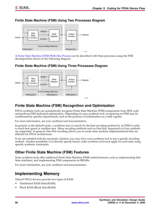
If you disable resource sharing, or if you code the design with the adders in separate processes, the design is
implemented using two separate modules as shown in the following diagram.
Synthesis and Simulation Design Guide
UG626 (v 11.4) December 2, 2009 www.xilinx.com 91](https://image.slidesharecdn.com/sim-120220090038-phpapp01/85/Sim-91-320.jpg)
![Chapter 5: Coding for FPGA Device Flow
VHDL Primitive Attribute Coding Example
The following VHDL coding example shows an example of setting the INIT primitive attribute for an instantiated
RAM16X1S which will specify the initial contents of this RAM symbol to the hexadecimal value of A1B2.
small_ram_inst : RAM16X1S
generic map (
INIT => X"A1B2")
port map (
O => ram_out, -- RAM output
A0 => addr(0), -- RAM address[0] input
A1 => addr(1), -- RAM address[1] input
A2 => addr(2), -- RAM address[2] input
A3 => addr(3), -- RAM address[3] input
D => data_in, -- RAM data input
WCLK => clock, -- Write clock input
WE => we -- Write enable input
);
Verilog Primitive Attribute Coding Example
The following Verilog coding example shows an instantiated IBUFDS symbol in which DIFF_TERM and
IOSTANDARD are specified as FALSE and LVDS_25 respectively.
IBUFDS #(
.CAPACITANCE("DONT_CARE"), // "LOW", "NORMAL", "DONT_CARE" (Virtex-4/5 only)
.DIFF_TERM("FALSE"), // Differential Termination (Virtex-4/5, Spartan-3E/3A)
.IBUF_DELAY_VALUE("0"), // Specify the amount of added input delay for
// the buffer, "0"-"16" (Spartan-3E/3A only)
.IFD_DELAY_VALUE("AUTO"), // Specify the amount of added delay for input
// register, "AUTO", "0"-"8" (Spartan-3E/3A only)
.IOSTANDARD("DEFAULT") // Specify the input I/O standard
) IBUFDS_inst (
.O(O), // Buffer output
.I(I), // Diff_p buffer input (connect directly to top-level port)
.IB(IB) // Diff_n buffer input (connect directly to top-level port)
);
Passing Synthesis Constraints
This section discusses Passing Synthesis Constraints, and includes:
• About Passing Synthesis Constraints
• Passing VHDL Synthesis Attributes
• Passing Verilog Synthesis Attributes
About Passing Synthesis Constraints
A constraint can be attached to HDL objects in your design, or specified from a separate constraints file. You can
pass constraints to HDL objects in two ways:
• Predefine data that describes an object
• Directly attach an attribute to an HDL object
Predefined attributes can be passed with a COMMAND file or constraints file in your synthesis tool, or you can
place attributes directly in your HDL code.
This section illustrates passing attributes in HDL code only. For information on passing attributes via the
command file, see your synthesis tool documentation.
Synthesis and Simulation Design Guide
UG626 (v 11.4) December 2, 2009 www.xilinx.com 95](https://image.slidesharecdn.com/sim-120220090038-phpapp01/85/Sim-95-320.jpg)

![Chapter 7: Simulating Your Design
Using the VOLTAGE and TEMPERATURE Constraints
Prorating is a linear scaling operation. It applies to existing speed file delays, and is applied globally to all
delays. The prorating constraints, VOLTAGE and TEMPERATURE, provide a method for determining timing delay
characteristics based on known environmental parameters.
For more information on the VOLTAGE and TEMPERATURE constraints, see the Constraints Guide.
Using the VOLTAGE Constraint
The VOLTAGE constraint provides a means of prorating delay characteristics based on the specified voltage
applied to the device. The User Constraints File (UCF) syntax is:
VOLTAGE=value[units]
where
• value is an integer or real number specifying the voltage
• units is an optional parameter specifying the unit of measure.
Using the TEMPERATURE Constraint
The TEMPERATURE constraint provides a means of prorating device delay characteristics based on the specified
junction temperature. The UCF syntax is:
TEMPERATURE=value[C|F|K]
where
• value
is an integer or a real number specifying the temperature
• C, F, and K are the temperature units
– C = degrees Celsius (default)
– F = degrees Fahrenheit
– K = degrees Kelvin
The resulting values in the Standard Delay Format (SDF) fields when using prorated VOLTAGE and
TEMPERATURE values are the prorated worst case values.
Determining Valid Operating Temperatures and Voltages
To determine the specific range of valid operating temperatures and voltages for the target architecture, see the
device data sheet. If the temperature or voltage specified in the constraint does not fall within the supported
range, the constraint is ignored and an architecture specific default value is used instead.
Not all architectures support prorated timing values. For simulation, the VOLTAGE and TEMPERATURE
constraints are processed from the User Constraints File (UCF) into the Physical Constraints File (PCF). The PCF
must then be referenced when running NetGen in order to pass the operating conditions to the delay annotator.
To generate a simulation netlist using prorating for VHDL, type:
netgen -sim -ofmt vhdl [options ] -pcf design.pcf .ncddesign
To generate a simulation netlist using prorating for Verilog, type:
netgen -sim -ofmt verilog [options ] -pcf design.pcf design.ncd
Combining both minimum values overrides prorating, and results in issuing only absolute process MIN values
for the simulation Standard Delay Format (SDF) file.
Prorating is available for certain FPGA devices only. It is not intended for military and industrial ranges. It is
applicable only within commercial operating ranges.
Synthesis and Simulation Design Guide
138 www.xilinx.com UG626 (v 11.4) December 2, 2009](https://image.slidesharecdn.com/sim-120220090038-phpapp01/85/Sim-138-320.jpg)


![Appendix C: Simulating Xilinx Designs in Synopsys VCS-MX and Synopsys VCS-MXi
Three-Step Process Analysis Phase
The three-step process analysis phase consists of:
• vlogan [vlogan_options] file2.v file3.v file4.v
Analyze all Verilog files except the top-level Verilog file.
• vhdlan [vhdlan_options] file5.vhd file6.vhd
Analyze the VHDL bottom-most entity first, then move up in order.
Three-Step Process Elaboration Phase
The three-step process elaboration phase consists of:
vcs [vcs_options] entity
Three-Step Process Simulation Phase
The three-step process simulation phase consists of:
simv [simv_options]
For more information, see the VCS User Guide, located in your VCS install directory at
VCS_HOME/doc/UserGuide/vcsmx_ug_uum.pdf.
Using Standard Delay Format (SDF) with VCS
There are two methods for back annotating delay values from an Standard Delay Format (SDF) file:
• Compiling the Standard Delay Format (SDF) file at Compile Time
• Reading the ASCII Standard Delay Format (SDF) File at Runtime
Compiling the Standard Delay Format (SDF) file at Compile Time
To compile the Standard Delay Format (SDF) file at compile time, run the +compsdf option as follows:
vcsi -R -f options.f +compsdf
VCS defaults to an SDF file that has the same name as the top-level simulation netlist. To use a different SDF
file, specify the SDF file name after the +compsdf option. No table files are required on the command line. VCS
automatically determines the required capabilities.
Reading the ASCII Standard Delay Format (SDF) File at Runtime
To read the ASCII Standard Delay Format (SDF) file at runtime, you must provide a table file with the -P option
as follows:
1. Create a PLI table file (sdf.tab) that maps the $sdf_annotate system task to the C function
sdf_annotate_call.
2. Use the -P option to specify this file as follows:
vcs -P sdf.tab -y $XILINX/verilog/src/simprims +libext+.v time_sim.v
Following is an example of an entry in the sdf.tab file:
$sdf_annotate call=sdf_ annotate_ call acc+=tchk, mp, mipb:%CELL+
Synthesis and Simulation Design Guide
UG626 (v 11.4) December 2, 2009 www.xilinx.com 171](https://image.slidesharecdn.com/sim-120220090038-phpapp01/85/Sim-171-320.jpg)